Autore:
Francesco Sechi _______________
Relatori:
Prof. Luca Fanucci _______________
Prof. Roberto Saletti _______________
FLEXIBLE LOW-COST HW/SW
ARCHITECTURES FOR TEST,
CALIBRATION AND CONDITIONING
OF MEMS SENSOR SYSTEMS
Anno 2011 SSD ING-INF/01
UNIVERSITÀ DI PISA
Scuola di Dottorato in Ingegneria “Leonardo da Vinci”
Corso di Dottorato di Ricerca in
INGEGNERIA DELL’INFORMAZIONE
A Simona
Alla mia famiglia
ACKNOWLEDGMENTS
A lot of people attend me for the whole period of my PhD course, but some in particular deserve a special thanks.
I would like to say thank you to my parents and my sisters for their essential support: I would have never reached this goal without your protection and the warmth of your words.
Another very important person I would like to thank you is Simona, because her love gave me the strength to get over all the difficulties I met during this period. Then my gratitude goes to my tutors Prof. Luca Fanucci and Prof. Roberto Saletti both for their precious technical help and for the several chances of professional improving they provided to me.
A special thanks goes to the SensorDynamics’ design center of Navacchio, particularly to Alessandro Rocchi and Adolfo Giambastiani for their precious technical and professional teaching, and for giving me the chance to explore the amazing world of electronic!
Last but not least, a great thanks goes to all my friends, especially to Sergio, Alberto, Chiara, Marcolino, Weiwor, Claudioca’, Agostino, Paolo and Fabio&Enrica, and to all my cousins and relatives.
SOMMARIO
Negli ultimi anni gli smart sensor basati su sistemi Micro-Elettro-Meccanici (MEMS) si sono largamente diffusi in diversi settori quali l’Automotive, il settore biomedico, quello ottico e il consumer, e oggigiorno rappresentano il più avanzato stato dell’arte. Le ragioni della loro diffusione sono legate alla loro capacità di misurare quantità fisiche e chimiche usando componenti miniaturizzati.
Lo sviluppo di questo tipo di architetture, per via della eterogeneità delle loro componenti, richiede un flusso di progetto molto più complesso per via della presenza sia di parti meccaniche proprie del sensore MEMS, sia di componenti elettroniche per l’interfacciamento e il condizionamento.
In questo tipo di sistemi acquista una notevole rilevanza l’attività di testing, che interessa varie fasi del ciclo di vita di un sistema basato su sensori MEMS. Infatti, sin dalla fase di design del sensore è importante validare il progetto estraendone i parametri caratteristici, che saranno utili durante la fase di design del circuito di interfaccia e condizionamento. Inoltre, un’architettura di questo tipo richiede, oltre ai tradizionali metodi di test che riguardano la circuiteria di controllo, anche tecniche per la calibrazione e la valutazione dell’intero sistema.
La prima parte di questo lavoro di ricerca affronta il tema dell’ottimizzazione del testing mediante lo sviluppo di differenti architetture hardware/software per le diverse fasi di test che fanno parte del flusso di sviluppo di un sistema basato su sensori MEMS. E’ stata sviluppata una piattaforma flessibile e a basso costo per la caratterizzazione e la prototipazione di sensori MEMS, così da offrire un ambiente che permetta inoltre di supportare la progettazione dell’interfaccia per sensore. Per ridurre il tempo di ingegnerizzazione richiesto durante la fase di ―verification testing‖ è stata progettata un’architettura client-server universale che offre un unico framework per il test di diversi tipi di dispositivi, permettendo l’utilizzo di differenti tipi di ambienti di sviluppo e linguaggi di programmazione. Dato che l’uso di macchine ATE durante lo sviluppo dell’algoritmo di calibrazione è costoso in termini di tempo di occupazione della macchina stessa, poiché un suo utilizzo durante questa fase richiederebbe la sospensione del processo di produzione, si è proposta un’architettura hardware/software a basso costo e facilmente adattabile per la calibrazione e la valutazione delle performance che consente lo sviluppo dell’algoritmo di test in un ambiente user-friendly e permette inoltre di realizzare una produzione su piccola e media scala.
Nella seconda parte del lavoro di ricerca si è approfondito un argomento che sta acquisendo una sempre maggiore importanza nell’ambito dello sviluppo di applicazioni per sensori MEMS, e riguarda la possibilità di combinare le informazioni estratte da diversi tipologie di sensori (tipicamente accelerometri, giroscopi e magnetometri) per ottenere informazioni più complesse. In questo contesto sono stati sviluppati e analizzati due differenti algoritmi di sensor fusion: il primo è un algoritmo puramente software che è stato utilizzato come strumento per valutare quanto un errore nella misura del MEMS può inficiare la stima del parametro calcolato usando un algoritmo di sensor fusion; il secondo, invece, è un algoritmo di sensor fusion basato su un filtro di Kalman semplificato. Di questo algoritmo è stato creato anche un modello bit-true in Mathworks SimulinkTM che verrà usato come studio di sistema per l’implementazione dell’algoritmo su chip.
ABSTRACT
During the last years smart sensors based on Micro-Electro-Mechanical systems (MEMS) are widely spreading over various fields as automotive, biomedical, optical and consumer, and nowadays they represent the outstanding state of the art. The reasons of their diffusion is related to the capability to measure physical and chemical information using miniaturized components.
The developing of this kind of architectures, due to the heterogeneities of their components, requires a very complex design flow, due to the utilization of both mechanical parts typical of the MEMS sensor and electronic components for the interfacing and the conditioning.
In these kind of systems testing activities gain a considerable importance, and they concern various phases of the life-cycle of a MEMS based system. Indeed, since the design phase of the sensor, the validation of the design by the extraction of characteristic parameters is important, because they are necessary to design the sensor interface circuit. Moreover, this kind of architecture requires techniques for the calibration and the evaluation of the whole system in addition to the traditional methods for the testing of the control circuitry.
The first part of this research work addresses the testing optimization by the developing of different hardware/software architecture for the different testing stages of the developing flow of a MEMS based system. A flexible and low-cost platform for the characterization and the prototyping of MEMS sensors has been developed in order to provide an environment that allows also to support the design of the sensor interface. To reduce the reengineering time requested during the verification testing a universal client-server architecture has been designed to provide a unique framework to test different kind of devices, using different development environment and programming languages. Because the use of ATE during the engineering phase of the calibration algorithm is expensive in terms of ATE’s occupation time, since it requires the interruption of the production process, a flexible and easily adaptable low-cost hardware/software architecture for the calibration and the evaluation of the performance has been developed in order to allow the developing of the calibration algorithm in a user-friendly environment that permits also to realize a small and medium volume production.
The second part of the research work deals with a topic that is becoming ever more important in the field of applications for MEMS sensors, and concerns the capability to combine information extracted from different typologies of sensors (typically accelerometers, gyroscopes and magnetometers) to obtain more complex information. In this context two different algorithm for the sensor fusion has been analyzed and developed: the first one is a fully software algorithm that has been used as a means to estimate how much the errors in MEMS sensor data affect the estimation of the parameter computed using a sensor fusion algorithm; the second one, instead, is a sensor fusion algorithm based on a simplified Kalman filter. Starting from this algorithm, a bit-true model in Mathworks SimulinkTM has been created as a system study for the implementation of the algorithm on chip.
TABLE OF CONTENTS
INDEX OF FIGURES ... IX INDEX OF TABLES ... XI
INTRODUCTION ... 1
1 TESTING OF MIXED-SIGNAL MEMS SENSOR SYSTEMS ... 5
1.1 Introduction... 5
1.1.1 Applications ... 6
1.1.2 Design and testing of a MEMS based devices ... 8
1.2 Design of MEMS sensors ... 10
1.2.1 MEMS modeling ... 11
1.2.2 MEMS layout ... 13
1.3 Design of the conditioning system ... 14
1.3.1 Microsystem vs. Micromodule ... 15
1.3.2 Functions of a microsensor system ... 15
1.3.3 Typical microsensor interface circuit ... 17
1.4 Testing and characterization of the SoP ... 19
1.4.1 Type of testing ... 20
1.4.2 Automatic test equipment... 21
1.4.3 Testing of sensor systems ... 22
1.5 Calibration and performances evaluation ... 22
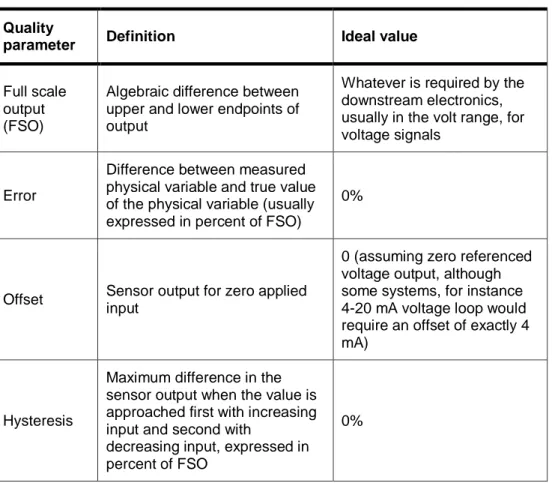
1.5.1 Performance parameters and sensor errors ... 23
1.5.2 Sensor calibration ... 25
1.5.3 Calibration of inertial sensors ... 26
1.6 The future of MEMS based systems ... 29
2 CHARACTERIZATION OF MEMS AND PROTOTYPING OF THE SENSOR INTERFACE ... 31
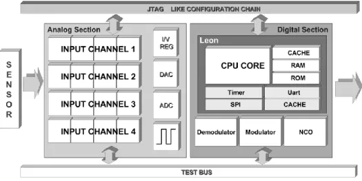
2.1 ISIF: a low-cost and flexible platform for the characterization and the conditioning of MEMS sensors ... 32
2.1.1 ISIF platform ... 32
2.1.1.1 Analog section ... 33
2.1.1.2 Digital section ... 33
2.1.1.3 Software ... 34
2.1.1.4 High Voltage Board ... 35
2.1.2 Fast-developing and low-cost characterization and test environment ... 35
2.1.3 Test and characterization of a double axis resonating micromirror
36
2.1.3.1 Physical description and principle of operation of the micromirror ... 36
2.1.3.2 Electrostatic FEM simulations ... 37
2.1.3.3 Mechanical Simulations for the resonance frequency extraction ... 39
2.1.3.4 Mechanical Simulations for the K extraction ... 40
2.1.3.5 Electrical Model ... 42
2.1.3.6 SimulinkTM model ... 44
2.1.4 Test and characterization with ISIF flow ... 46
2.1.4.1 Setup and static capacitance measurement ... 47
2.1.4.2 Dynamic ΔC measurements ... 47
2.2 Pin-limited frequency converter bridge for fast prototyping of custom functionalities in platform-based sensor interfaces ... 50
2.2.1 State of the Art Review ... 50
2.2.2 Project Design Flow ... 51
2.2.3 IP Bridge Architectural Design ... 51
2.2.4 Implementation and test results ... 58
2.2.5 Case Study of an Automotive Smart IC Sensor ... 59
2.3 Conclusions... 61
3 VERIFICATION TESTING AND CALIBRATION ... 63
3.1 Universal communication framework: DevCom ... 64
3.1.1 State of the art ... 64
3.1.2 Architecture ... 65
3.1.2.1 Overall description ... 65
3.1.2.2 Server ... 67
3.1.2.3 Client ... 68
3.1.3 DevCom for SD sensors ... 68
3.1.3.1 SD74x series inertial sensors ... 68
3.1.3.2 FTDI driver ... 69
3.1.3.3 Applications ... 70
3.2 Low-cost architecture for the calibration and evaluation of IMSS for small and medium volumes production: CaLVal ... 70
3.2.1 Overall description ... 70 3.2.2 Hardware design ... 71 3.2.3 Software design ... 73 3.2.3.1 Instruments ... 73 3.2.3.2 Communication layer ... 74 3.2.3.3 Test procedures ... 74
3.2.3.4 Single piece application ... 75
3.2.3.5 Logging and Yield Management System ... 76
3.3 Conclusions... 80
4 DATA PROCESSING ... 83
4.1 A preliminary evaluation using a fully software algorithm ... 83
4.1.1 Overview ... 83
4.1.2 The architecture ... 84
4.1.2.1 Hardware and Firmware ... 84
4.1.2.2 Software ... 85
4.2 An integrated sensor fusion algorithm for the orientation tracking .... 90
4.2.1 State of the art ... 90
4.2.2 System modelling ... 90
4.2.3 Algorithm simplifications ... 93
4.2.4 Simulations ... 94
4.2.5 Bit true model ... 97
4.3 Conclusions... 98
5 CONCLUSIONS ... 99
INDEX OF FIGURES
Figure 1-1. MEMS market forecast [1] ... 6
Figure 1-2, Flowchart of the life cycle of a MEMS system ... 9
Figure 1-3. MEMS design flow block diagram ... 11
Figure 1-4. Schematic representation of a MEMS physical process ... 13
Figure 1-5. Functions of a sensor system ... 16
Figure 1-6. Block diagram of a generic sensor interface... 17
Figure 1-7. Basic principle of digital testing ... 20
Figure 1-8. Test machines: (A) Accelerometer turntable; (B) Two-axis rate table; (C) Vibration machine [3] ... 27
Figure 1-9. Motion sensor combos: strategies of integration [2] ... 29
Figure 2-1. ISIF block diagram ... 32
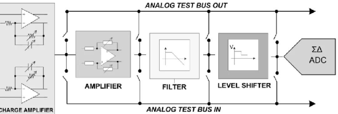
Figure 2-2. Input channel block diagram ... 33
Figure 2-3. Signal chain ... 34
Figure 2-4. LabVIEWTM GUI ... 36
Figure 2-5. Micromirror structure ... 37
Figure 2-6. Simplified structure used for electrostatic simulations ... 38
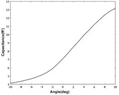
Figure 2-7. Capacitance versus angle relationship for the micromirror fast axis ... 39
Figure 2-8. Fast axis motion at its resonance frequency ... 40
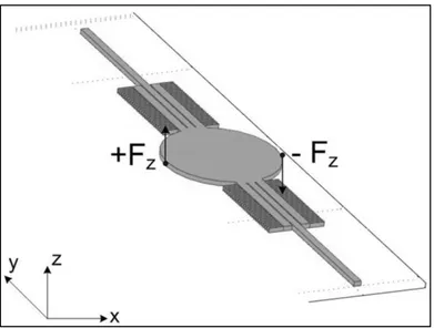
Figure 2-9. Forces applied to the micromirror plate ... 41
Figure 2-10. Mechanical Torque versus rotation angle for the fast axis... 42
Figure 2-11. (a) Micromirror layout; (b) Slow axis model ... 43
Figure 2-12. Block diagram of the SimulinkTM model for the micromirror fast axis 45 Figure 2-13. Rotation angle versus time curve for the micromirror fast axis ... 46
Figure 2-14. Test and Characterization setup ... 47
Figure 2-15. Digital amplitude of the sensing signal versus frequency extracted from the open loop analysis on slow axis ... 48
Figure 2-16. Maximum deflection angle versus driving frequency extracted from the open loop analysis on slow axis ... 49
Figure 2-17. Maximum deflection angle versus driving frequency extracted from the open loop analysis on fast axis ... 49
Figure 2-18. Closed loop driving block diagram ... 50
Figure 2-19. Bi-synchronous FIFO... 52
Figure 2-20. IP bridge pinout ... 53
Figure 2-21. IP bridge architecture ... 54
Figure 2-22. Meaning of pinout in transaction from ASIC to FPGA... 57
Figure 2-23. Meaning of pinout in transaction from FPGA to ASIC... 57
Figure 2-24. Bridge area vs. different size of the FIFOs ... 59
Figure 2-25. Bridge slack time and area vs. temperatures and supply voltages ... 60
Figure 2-26. Micromirror ASIC and FPGA connection through bridge ... 61
Figure 3-1. Block diagram of DevCom architecture ... 65
Figure 3-2. Hypothetical scenario of DevCom architecture ... 66
Figure 3-3. Board for SD sensor communication ... 69
Figure 3-4. Motors movements in CaLVal ... 71
Figure 3-5. Board block diagram... 72
Figure 3-7. Test procedure template... 75
Figure 3-8. Front-end of the YMS manager ... 77
Figure 3-9. Software layers including SD74x family components ... 78
Figure 3-10. Flow chart of (a) trimming (b) performance ... 79
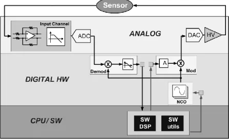
Figure 4-1. 3D view of the board... 84
Figure 4-2. Block diagram of the board ... 85
Figure 4-3. Rotation algorithm flowchart ... 87
Figure 4-4. Acceleration algorithm and cross-compensation flowchart ... 88
Figure 4-5. Kalman filter algorithm. ... 92
Figure 4-6. SensorDynamics Cube Demo sensor... 94
Figure 4-7. Drift on the x axis ... 95
Figure 4-8. Drift correction on the x axis with the Kalman filter ... 95
INDEX OF TABLES
Table I – Performance parameters ... 23 Table II – Resonance frequencies for the micromirror fast axis ... 40 Table III – Comparison between simulation results and test results (slow axis) .... 62 Table IV – Device access right ... 68 Table V – Example of limit file for trimming stage ... 80 Table VI – Rotation sequence ... 96 Table VII – Mean square error related to the number of bits used for data representation ... 97
INTRODUCTION
Micro-electro-mechanical-systems (MEMS) technology is widely spreading during the last years, also thanks to the employment in the consumer applications.
MEMS devices can be defined as micrometers embedded systems whose purpose is to collect physical and chemical information of various kinds about their environment and to make this information available in a form more suitable for the human senses and technical systems.
The design of this kind of devices is very challenging, but also testing activity has a key role in the development of MEMS based device, because of the complexity of a MEMS system architecture that is composed by heterogeneous elements, and each one of these components requires a different approach to verify its correctness.
A MEMS device, in fact, is composed by electrical and mechanical parts, so it requires different test equipment to perform electrical testing and mechanical testing. MEMS testing and reliability assurance are critical processes to achieve high yields and profitability as these processes account for 40 to 70% of the total device cost.
In order to reduce this cost, the main key factor can be identified as the standardization of the test equipment. Indeed, most of the MEMS testing is performed separately for electrical and mechanical elements. This market scenario is changing and there are several test vendors developing key solutions to perform both the electrical and mechanical testing in a single test equipment. Another challenge prevailing in the market today is the non-availability of standardized equipment to test the MEMS devices cost effectively. In fact, current test equipment is priced as high as $1 million, which can deter most MEMS device manufacturers from testing their products. Since customized solutions require vendors to conduct research every time they receive an order, they tend to be expensive. The costs are expected to drop once standard solutions become more prevalent. Most semiconductor industry engineers have a mechanical background or an electrical background, which is sufficient to test any type of semiconductor product. However, testing combined components is more complex than testing them separately, and not many have the technical training required to perform the tests.
To overcome the target of cost effective and time-to-market reduction, the standardization of the test equipment is not enough. Indeed, the life-cycle of a MEMS device consists on several steps, and almost all of these requires different approach to verify and validate its output product.
During the design of the MEMS, simulation and prototyping of the device are required. High volume, high-cost, and accurate measuring systems are necessary to characterize and test the designed device, especially to examine motions, deflections and resonance frequencies of the mechanical structures that are the distinguishing characteristics of these systems. A variety of custom systems relying on interferometry have been developed for deflection measurement but they require a significant amount of development time. Alternatively, there are a variety of commercial deflection measurement systems based on scanning Laser-Doppler
vibrometers. However, even though these systems feature very accurate results, they are often very expensive.
The design of the sensor interface circuit requires an high accurate simulation and validation, and often the use of CAD tools are not enough to verify the correctness of the design, because it is based on approximated models of the MEMS device, produced during the design of the MEMS itself. A solution to perform also a prototyping of the sensor interface will be appreciated, but, for the moment, no solution are commercially available to supply for this lack.
Once the sensor interface is developed, it must be tested. Different typologies of testing have done, depending on the phase of the life-cycle of a chip. The verification testing regards the certification of the correctness of the design and of the test procedure in laboratory, and it is done the first time the chip is designed and fabricated. The manufacturing testing, instead, regards the testing of the fabricated chip in the factory during the production phase. Each device has its own pinout, its interface, and its peculiar characteristic, so the verification testing requires to set up a custom device each time a new device is developed. This reengineering activity entails a growth of costs and time-to-market. So, the reengineering time must be reduced as much as possible, standardizing the applications that interact with the device to provide a common interface that allows to reuse the same tests developed for other products. Some applications are available in the marketplace to achieve this goal, but all of these suffer from different drawbacks, as incompatibility, non concurrent access to the device, absence of libraries to manage laboratory instruments, and so on. The use of this approach, moreover, permits to define the test program directly in the laboratory, reducing the time a test machine is used to debug the test procedure.
The last step of the production flow is the design of the calibration algorithm. The calibration is the procedure of correcting the transfer function of a sensor, using a reference measurement system in order to guarantee a specified input-output relationship with a certain accuracy and under certain conditions. To calibrate a sensor, it is necessary to excite it with an appropriate physical stimulus. To do so, a test machine able to produce this stimulus is necessary. To calibrate a sensor, very expensive test machines are used. These machines allow to calibrate different pieces contemporarily and to handle the socketing of each piece automatically, in order to calibrate pieces continuously. The cost of this machine can be quantified in terms of cost for the equipment and cost for the usage time. While the first one depends on the machine vendor, the second one is dependent on the allocation time disposed by the MEMS device developer. So, in order to minimize the costs, a solution to avoid the use of the production machine for the debug of the calibration algorithm is desirable.
Besides the problematic concerning the development of these smart sensors, the diffusion of this kind of technology in consumer electronic application is causing a continuous demand for new functionalities together with the one offered by the sensors themselves. In fact, differently to other fields the MEMS were traditionally used, the consumer field is very dynamic and requires a continuous innovation in the offered functionalities in order to keep up with the competitors. In the last few years, sensor fusion algorithms, used to combine the outputs of different kind of sensor in order to produce new information, are identified as the future of
microsensor technology, and different companies are equipping their devices with components that implement functionalities on the basis of these algorithms.
This research work deals with two main topics: the first is the development of hardware and software architecture for the optimization of the verification and validation stages in terms of cost effectiveness and time-to-market reduction; the second concerns the analysis and the developing of sensor fusion algorithms. Chapter 1 presents the MEMS technology by describing its historical development and the fields of applications, then the fundamental steps that characterize the life-cycle of a MEMS are illustrated. The chapter is then concluded by showing the trend of this technology for the next future.
The first part of chapter 2 illustrates a flexible and low-cost platform for the characterization and the prototyping of MEMS sensors. This architecture permits to reduce the time for simulating complex characteristic parameters combining the simulation data with measurements. Moreover, its high reconfigurability permits also to use it for the evaluation of the required sensor interface. The second part describes a pin limited frequency converter bridge for the communication between an ASIC and a FPGA. This architecture is very important during the prototyping phase because it permits to design new functionalities without the need to redesign the ASIC.
The first part of chapter 3 describes a solution for the optimization of the validation phase of the packaged device. The proposed architecture offers a standard framework for the developing of the test environment in laboratory, permitting to reuse the same setup for different systems. The second part shows a low-cost architecture for the calibration of MEMS sensor systems that permits the debugging of a calibration algorithm without using a complex ATE.
Chapter 4 deals with the analysis of algorithm for sensor fusion. In particular, after a brief analysis of the advantages and disadvantages of a purely software development, a solution for an integrated angular position estimation is illustrated. A simplified Kalman filter has been used in order to permit the integration in the sensor interface integrated circuit.
1
TESTING OF MIXED-SIGNAL MEMS SENSOR SYSTEMS
1.1 Introduction
Micro electromechanical systems (MEMS) are probably the smallest functional machines that are currently engineered by humans. They can be defined as embedded systems involving both electronic and mechanical components with a dimensional scale of the order of micrometers and that employ both an electronic movement of charge and mechanical movement for operation. The purpose of microsensors is to collect physical and chemical information of various kinds about their environment and to make this information available in a form more suitable for the human senses and technical systems.
MEMS device development can be traced back to the 1970's, but the first microsensor was developed in 1956, thanks to the discovery of the piezoresistive effect in silicon and germanium. However, it is in the period since 1995 that this technology caught on, because a wide range of new materials and bulk micromachining technologies have become available. Business and scientific world were very interested in MEMS technology, and also many governments heavily funded the research in this field. The reasons for this attention were numerous: first of all, the cost of this technology is reduced, because it scales with its size; second, MEMS devices are characterized by excellent mechanical properties, due to their pure crystalline structure; moreover, they can be fabricated using the same technology infrastructure of the integrate circuit (IC) industry; finally, MEMS devices can be integrated with IC circuitry to create low cost systems on a chip. All these reasons contribute to the proliferation of this technology, particularly the possibility to integrate different components together to perform more complex functionalities. For instance, a single device can integrate multiple sensors and combine the information they produce to extract other kind of information, like position, combining a 3-axis gyroscope and a 3-axis accelerometer.
MEMS is a potent technology and its powerful expresses especially in sensor application. There is now the possibility of designing complex MEMS based systems able to sense and react to their environment and respond and adapt to it. However, even though MEMS technology has been very promising, commercialization efforts have encountered multiple stumbling blocks that have significantly delayed the availability of commercial devices. A first stumbling block was the fact that the IC industry has not provided all process modules required to fabricate mechanical devices (such as wafer deep etching, double side wafer alignment and multiple wafer bonding) and the development of such MEMS processes was long and expansive. Secondly, the mechanical properties of IC materials were unknown and dependent on the fabrication process as well as electrical stability of silicon structures. The third point is that in the IC industry the structure thickness was not an issue, IC industry required an accuracy on thickness of about ±10%, but in MEMS industry the thickness becomes a key point and a better control for mechanical thickness is required. Moreover high volume, low cost MEMS dedicated testing had to be developed entirely by the MEMS industry. And finally the compatibility with the real world was the major task to be developed by MEMS industry.
Despite of this problems, MEMS technology importance in the electronic marketplace is increasing rapidly, particularly during the last years. Figure 1-1 shows the trend of the market for this kind of technology.
Figure 1-1. MEMS market forecast [1]
The sector will likely see a healthy increase this year despite any general semiconductor slowdown, and will remain on track to maintain its 17% average growth for the next years. This charge in volume production is owing to the wide spreading of these devices also in consumer market. By 2012, MEMS makers will be shipping 8.1 billion units a year, worth some $15.5 billion, and nearly half that market will be consumer devices. Major market drivers will include silicon microphones, micro displays, RF MEMS and even microfluidics for biomedical applications. RF MEMS and silicon microphones alone will account for more than 45% of unit demand from 2011.
1.1.1 Applications
With the consolidation of the MEMS technology, it spread in various fields, becoming the outstanding state of the art for a broad range of mechanical, chemical, optical, and biotech products (sensors, microstructures and actuators) fabricated as integrated circuits on silicon wafers in a batch mode. Commercial MEMS products comprise flow sensors, pressure sensors, acceleration sensors, gyros, ink-jet nozzles, head locators in hard drives, and digital light processors (DLPs) in projectors and screen sets. In the following an overview of the major field of applications for MEMS sensor is presented.
Life science applications
The requirement of reliable and very small implantable devices, and the need of handheld devices for patient monitoring and diagnostics at home brought to the utilize of this technology in medicine applications, creating a separated branch of devices called bioMEMS. Biocompatibility, reliability, miniaturization, low power are some of the advantages of this technology. Moreover, bioMEMS feature non invasive/painful procedures and allow to reduce the patient recovery time because they permit to monitor continuously the patient also outside the hospital. One of the most important segment for medical applications of MEMS is the so called Lab-on-a-chip (LOC) which is a typology of devices that integrate multiple laboratory functions on a single small device and that are able to manage extremely small fluid volumes.
Communications
Radiofrequency and microwave MEMS applications are introducing a important surplus value in wireless communications. Low loss, high Q-factor, high linearity and a good power handling are all the MEMS features that make this technology more suitable for this kind of applications with respect to traditional implementations. The use of MEMS in this field permits to produce wireless handsets, base stations and satellites with the key properties of low-power consumption, low area occupation and enhanced re-configurability, which can result in superior functionalities and performances.
Automotive
Electronic technologies in the automotive industry have been introduced starting from the 1960s, gradually replacing mechanical systems and hydraulic actuators. Today, high-end vehicles feature up to 100 different sensors among which about 30 these are now MEMS, and the percentage is forecasted to grow. Some of the main sensing applications in the automotive sector concern the active safety (ABS, ESP, TCS, and so on), intelligent light positioning, intelligent airbags, vehicle monitoring, satellite navigation systems and enhanced antitheft systems. To implement these automatic controls, gyroscopes and accelerometers are the most used MEMS devices.
Commercial applications
MEMS application are well established in specialized markets, primarily automotive, industrial and medical, and the conditions are mature for impacting the consumer market for a wide spectrum of applications. Some of these are ink-jet print heads, silicon microphones, hard disk drive free fall protection, gaming interfaces and digital still camera image stabilization. The consumer market is looking for tiny, low cost, low-power consumption devices. Consumer devices are all battery-operated and are becoming smaller and thinner. Furthermore, the product life cycle of consumer devices is shorter than the one in automotive markets; therefore, this make MEMS system suppliers to face an increasing reduction in time to market for developing new products.
Industrial applications
Requirements for safety in workplaces requires ah high accuracy of the sensing solution used to detect the dangerous operating conditions. MEMS technology supply these requirements, so also in industrial applications like safety systems, process control, equipment position, impact detection and environmental monitoring this technology has been widely used in the later years. Recently, another industrial segment grown significantly: the so called micro-drives. These micromechatronic systems consist of elements capable of processing information and energy and can be employed for fine refinements and advanced operations in which extreme accuracy is required. Moreover, MEMS devices are also used in instruments for synthesizing and analyzing (bio)chemical materials of higher quality, at higher throughputs and against reduced costs. Finally, MEMS devices can be effectively employed for industrial robots, as the technology can apply to tactile sensors, navigation, or proximity sensors.
Military and aerospace applications
Military and aerospace fields were the first major users of the MEMS technology. MEMS technology has enabled smaller, low power, and low cost micro-instruments currently including pressure, flow rate, acceleration, angular velocity, and MEMS actuators such as valves, synthetic jets, boundary layer trip devices, micro jet engines and microthrusters that have supported a variety of aerospace missions. Some of the major military and aerospace applications are microsatellites, micro-propulsion systems, navigation assistance and equipment monitoring,
Optical applications
A very important branch of MEMS family are the micro-opto-electro-mechanical systems (MOEMS). They were used for the first time in 1990 for fiber optic telecommunication applications, but, after a brief crisis, they started to be used in other kind of applications. The most important fields were MOEMS are employed are Digital Micromirror Devices (DMD) for the projection of images, spectrometers used to measure properties of light over a specific portion of the electromagnetic spectrum, barcode scanners, Infrared Focal Plane Array (IRFPA) for the image sensing, and picoprojectors.
1.1.2 Design and testing of a MEMS based devices
The design of a MEMS device is a very challenging activity, because requires a multidisciplinary approach due to the heterogeneity of its components. In fact, these components have mechanical, electrical, thermal, electrostatic, and fluidic interactions. This complexity requires structured design techniques to manage each activity involved in the design of this kind of devices. Although the design of the MEMS sensor(s) and of the sensor interface integrated circuit are crucial tasks for the success of the device, testing activities, that includes prototyping, characterization and calibration play a key role for the production of a winning product.
Figure 1-2 shows the fundamental steps that characterize the life-cycle of a MEMS based device. The design starts from an idea, arisen from market analysis, needs, lacks, and so on, an high level description is defined. It can include a block diagram of the components the device suppose to have and the interaction among them,
focusing on the target application the device will be designed to. Once the requirements are defined, both the MEMS and the sensor interface are developed. These steps are characterized by different activities that includes both design and testing tasks. In fact, the MEMS component, once designed, must be simulated and prototyped before starting to produce it. Likewise, the sensor interface, during the design and once the design is accomplished, must be simulated to verify its correctness. These two steps are strictly coupled, because the design of the sensor interface requires knowledge about the structure of the MEMS, particularly during the MEMS system modeling level (see paragraph 1.2.1). When both the sensor interface and the MEMS component(s) are developed, these components are packaged together. The type of packaging process depends on the adopted approach for the implementation of the microsensor system (see paragraph 1.3.1).
Figure 1-2, Flowchart of the life cycle of a MEMS system
The following step consists on the testing of all the functionalities of the device and its characterization. For a sake of simplicity in the representation of the flowchart
the characterization has been inserted after the packaging. Actually, the characterization involves different stages of the life cycle of the device. The purpose of the characterization is to verify that the design is correct and the device will meet all specifications, execute a so called test program to control an automatic test machine (see paragraph 1.4).
The last step before the production is the calibration. It consists on a set of measurements of the characteristic parameters when some appropriate stimuli are applied on the device and, on the basis of the measured value with respect to the data produced by a reference measurement unit, the characteristic transfer function is corrected in order to obtain a certain accuracy and under certain conditions.
The final step is the delivery to the customers. Also this step can be considered a testing activity, because the customer itself will test the device.
The next paragraphs describes all this steps in detail, focusing particularly on testing operation connected to the described activity.
1.2 Design of MEMS sensors
The design of MEMS sensors, as any complex engineering process, requires the definition of a formal design flow, in order to provide a structured and manageable design environment, to permit to spread a technology over a large audience and to formalize a detailed interface of each step and the interaction among them.
A good definition of a design flow allows to enable complex engineering design in the shortest time and through few fabrication iterations. For the definition of a MEMS sensor design flow the first approach was to embed the required design tools into a traditional analogical VLSI design flow. This solution, however, does not address the significant differences between the two technologies. VLSI design flow, in fact, almost exclusively involve a single physical domain: the electric domain, whereas MEMS design requires multiple domains. Moreover, while in VLSI modeling the layout is generated after modeling the functionality of the circuit, in MEMS design the layout itself (intended as geometry, orientation and position of the basic elements) is an essential component for the description of the functionality of a MEMS. For these reasons, the design flow for MEMS sensors requires an ad-hoc design flow.
The MEMS design flow block diagram is shown in Figure 1-3. Starting from the combination of the idea and a feasibility study based on a general architecture, the MEMS design flow begins with the product definition. During this phase, the device specifications, intended as sensitivity, noise, temperature stability and die size are defined. Costs are evaluated in this phase too. The next step consists on the developing of a Finite Element Method (FEM) model to define the MEMS geometry. This phase permits also to extract the characteristic device parameters by simulation, and this parameters are used to develop a high level MEMS model, used to start designing the sensor interface circuit (see paragraph 1.3). Once the MEMS geometry is completely defined and respects the device specifications, the device layout must be generated. To do so, usually the same tools used for the electronics layout are used. Before the production step is very important to perform the layout verification in order to discover and correct errors. This step consists of two actions: the verification of the match between the process specifications and
the layout realization through a Design Rule Check (DRC) and the verification of the compliance between the realized layout and the sensor schematic through a Layout Versus Schematic (LVS) check. Another optional step before production is the layout simulation (also called post layout simulations). This phase permits to verify the design correctness, and to tune the mechanical device properties used in the system level description to enhance the MEMS high level model. Moreover, simulating the geometry allows to find errors that are missed in previous models due to high approximations.
Figure 1-3. MEMS design flow block diagram
1.2.1 MEMS modeling
Modeling and analysis of devices and systems are complex subjects. Modeling occurs at many levels and uses a variety of modeling paradigms. Four modeling levels can be identified: System, Device, Physical and Process. All the levels are strictly coupled among them.
The top level is the system, in which the MEMS is modeled together with the sensor interface. In this level either of block diagram descriptions or lumped-element circuit models can be used. Both lead to a coupled set of ordinary differential equations (ODE) to describe the dynamical behavior of the system. Often these equations are written in a specific form as a coupled set of first-order ordinary differential equations for the state variable of the system. In this form the equations are referred as state equations for the system. The tool usually employed for system level models is SimulinkTM.
The bottom level is the process, in which the process sequence and photomask designs for device manufacturing are created. Process modeling at this level is a highly sophisticated numerical activity, so a number of commercial CAD tools have been developed: they are generically referred as technology CAD or TCAD. These CAD tools allow to predict device geometry from the mask and process sequence. However, the role of the designer is fundamental during this phase, because the correct material properties must be selected, and these properties depend on the detailed process sequence.
The physical level models the behavior of the real device in three dimensional continuum. The governing equations are partial differential equations (PDE), and various analytical models can be used to find closed-form solutions in ideal geometries; however, to model a realistic device it is necessary to use either approximate analytical solutions to the PDE’s or highly meshed numerical solutions. Different numerical modeling tools permits to simulate at the physical level, using either finite-element, boundary-element or finite-difference methods. However, to model electrostatic forces, mechanical behavior, coupled electro mechanics and damping effects commercial finite-element and boundary-element tools (for instance, AnsysTM and Comsol MultiphysicsTM) are necessary.
The device level is used to create a simplified model able to interact with the entire device and their associated circuitry. In fact, while the physical model is adapt to simulate the physical behavior, to interact with the system level without introducing excessive overload it is necessary to reduce a reduced order model. This model must be developed in a form that permits rapid calculation and insertion in a system level simulator. However, it must be energetically correct, conserving and dissipating energy when it should, have the correct dependence on material properties and device geometry, represent both static and dynamic device behavior for both small (linear) and large (non linear) amplitude excitation, and agree with the results of the 3D simulation of the physical level and with the results of experiments on suitable test structure.
There is no order in the developing of the different modeling levels: the designer can create models directly at the system level, or starting from one of the other levels. For example, the designer could start from a physical device description with all the device dimensions and the material properties and then use physical simulations tools to calculate device behavior, capture this behavior in a reduced order model and finally insert it into a system-level block diagram. Or alternatively the designer could simply use a parameterized reduced order model to represent a particular device and defer until later the specification on device dimensions to achieve the desired performance.
In conclusion, the operation of MEMS modeling is a fundamental step in MEMS design, because it permits to analyze the behavior of the sensor the designer is
going to build, evaluating also the interaction with the system it will be part of. This modeling phase allows to develop a mathematical representation of the MEMS sensor before building experimental prototypes, avoiding the costs of a wrong actual prototype. For this reason, modeling is also called ―numerical prototype‖.
1.2.2 MEMS layout
The MEMS layout is the last step before the device production. A MEMS process is based on the different steps of deposition, pattern and etching. A schematic representation is shown in Figure 1-4.
Figure 1-4. Schematic representation of a MEMS physical process
A structural layer of polysilicon (called epi poly and characterized by typical thickness of 11 um) is used to build the moving structure of the MEMS (light blue in figure). This moving structure is suspended over an etched pit and is anchored to the substrate with well defined anchor points. The position of these anchors define the MEMS motion which can be characterized by a rotating motion or/and a tilting motion. If the device is a capacitive structure, as the device shown in figure above, electrodes positioned under the moving structure are used to detect the motion through the capacitance variation between the moving structure and the electrodes themselves. The electrodes are made up of thin polysilicon (typical 100nm thick) defined as buried poly (blue layer in figure). The different signals are applied to the different mechanical structures by using appropriate connections between the mechanical parts and the MEMS pads. These connections are realized with both epi poly and buried poly paths which are vertically connected through ―vias‖. Since all MEMS processes are based on the same phases, it is possible to abstract them in a layered structure, where each layer represents a process step. Each process can be defined in terms of the manufacturing steps needed for each layer together with the characteristic properties of the material used and the geometrical dimensions of the layers. In the MEMS design methodology this information is
captured in a layout technology file and a layout design rules file which customize an appropriate layout tool. The tools used for this purpose were not originally intended for MEMS (e.g. Virtuoso tool of CadenceTM environment), so MEMS layout designers still face some common issues and roadblocks while attempting to create lithographic masks that correspond with the original device design, specifically in the areas of drawing, design rule checking (DRC) and output. In fact, these tools provide only rectangles as typical geometries, whereas MEMS structures involves arbitrary geometries like arcs, curves, and so on. In addition, in MEMS layout understanding the three-dimensionality of the topography is required. Moreover, while typical transistor blocks may cover 20x20 micrometers areas, MEMS geometries may have 5 micrometers features, and an overall dimension of 1mm. This wide range in size can result in constant zooming in and out during the design process. Thus, some MEMS designs require the ability to snap to corners, midpoints or user specified relative distances without zooming in. Finally, also the MEMS process requires DRC (Design rules check) and LVS (layout versus schematic check) to find errors before tape-out, but the same tools used for IC cannot be used for MEMS process because of the free-form nature of that, which requires to vary design rules depending on the MEMS fab and associated tooling, and many DRC tools are not able to perform operations on all-angle polygon geometries. So, the implementation of these tools also for MEMS is required to have a more reliable design flow.
1.3 Design of the conditioning system
The creation of the MEMS sensor is only the first phase of the develop of a sensor chip. In fact, the information produced by the MEMS must be converted into a form that may be easily manipulated by every components that could interact with it. So, it is necessary to design an electronic circuit able to do it, called sensor interface. The functions implemented by a sensor interface can range from simple amplification or filtering to A/D conversion, calibration, digital signal processing, interfacing with other electronic devices or displays, and data transmission (that can be handled by wired or, recently, wireless connection). Since the appearance of the first integrated circuit (IC), Very-large-scale integration (VLSI) technologies has been used to make sensor interface circuits, combining discrete sensors with application-specific integrate circuits (ASICs) or circuits on a printed circuit boards (PCB). With the birth of miniaturized sensors (microsensors), realized using IC technologies and materials, it has been possible to integrate the interface circuit and several sensors on the same chip or in the same packages, reducing the cost of measurement systems, the size of the whole system and its reliability.
However, the design of the sensor interface for microsensor systems is very complex for different reasons. This kind of systems, indeed, show worse performance due to weak signals and to offset and nonlinear transfer characteristics. Moreover, most of the traditional circuit techniques cannot be used because they rely on accurate component matching and complex analog functions that will make the device weak with respect to aging and degradation. In addition, it requires sensor specific design techniques to increase accuracy and to reduce the power consumption.
For these reasons, microsensor interface features are strictly coupled with the microsensor the interface must control and the package, because they depend heavily on the quantity to be measured, the physical effect used, the system architecture and the application.
1.3.1 Microsystem vs. Micromodule
There are two possible approaches for implementing microsensor systems: the microsystem approach and the micromodule approach [4]. In the microsystem approach, the sensor and the interface circuitry are integrated on the same chip, whereas, in the micromodule approach, the sensor and the interface circuitry are integrated on different chips, and they are included in the same package (SoP) or mounted on the same substrate.
Both the approaches have advantages and disadvantages. In the first approach, the microsensor must be designed taking into account the material characteristics given by the standard IC process used and any specific processing step has to be performed after the completion of the standard IC fabrication flow, limiting the possibility to improve the sensor performances. Moreover, there are also disadvantages about the cost and the yield. In fact, when the feature size of the technology reduces, while the cost per unit area of the IC is compensated by the area reduction, this is not true for the microsensor, because its size does not depend only on the technology, but also on physical constraints. In addition, the yield for a microsensor is generally lower than for ICs; so, having both elements in the same chip, force to discard a chip when a defect on the microsensor is discovered, even if the IC is working. However, this approach also has a lot of advantages. In fact, the system assembly is simple, inexpensive, and independent of the number of interconnection needed. Moreover, the parasitic due to the interconnections between the sensors and the interface are minimized, and also other parasitic effects are compensated by the use of the same technology that allows to achieve good matching between elements of the two components of the system.
In the second approach, it is possible to use different technology for the sensors and the interface, allowing to choose expensive submicron technologies for the IC and low cost technology for the sensor. Using two different materials, it is possible to optimize the performance separately, reducing the cost and increasing the yield. This approach, however, has a number of drawback. First of all, the assembling is quite expensive and it is a source of possible failures; moreover, the number of interconnections allowed between the sensors and the IC is limited, and these interconnections produces high and unpredictable parasitic. Finally, matching between elements of the sensor and elements of the interface circuitry cannot be guaranteed.
1.3.2 Functions of a microsensor system
As we already said in the introduction, the components of a sensor interface strictly depend on the quantity to be measured, the physical effect used, the system architecture and the application. So, it is more suitable to talk about functions instead of components [5, 8].
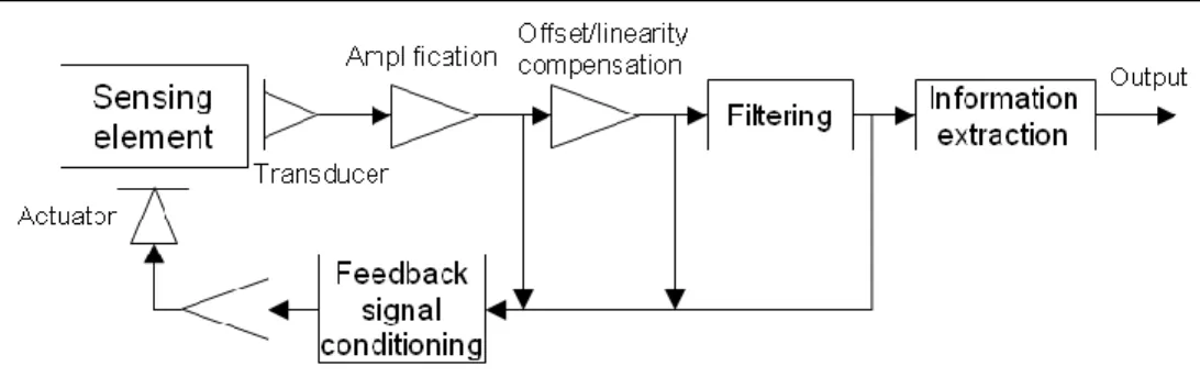
Figure 1-5 reports the set of function that constitutes the typical structure of a sensor interface. Each element represented in the figure can be implemented as
single component or subsystems or can be distributed in different components or sub-components. Moreover, some parts can be implemented also outside the sensor interface by the application that uses the system. The decisions as to which functions are implemented where form an important discussion in modern sensor systems design, and depend strictly on the designer choices and the target application. The scheme in figure, however, is not constraining, so some functions can miss and other functionalities can be implemented in the system. For example, while the forward chain is mandatory to extract the information from the MEMS sensor, not all the systems implement the feedback chain that is used only in the ―closed loop‖ sensor category.
Figure 1-5. Functions of a sensor system
A generic sensor system can be described starting from the sensing element, that can be defined as a component that receives the energy from the physical entity being sensed. This form of energy is converted to electrical energy by the transducer. As we already said in the introduction, microsensors produce weak signals, so it is necessary to increase the amplitude of the signals. The role of the amplification function is to translate an electrical signal to one of a different amplitude, that may be expressed as a voltage, a current or a charge. The amplification factor is the gain. Also the conversion between two signal forms (for instance from current to voltage) and the level translation within digital systems can be considered as part of the amplification function. The Offset/linearity compensation is the process of suppress the offset and nonlinearity, which can be originated from imperfection or the characteristic of the sensor itself, from the sensor characteristic. More details on the compensation process are described in paragraph 1.5. The filtering function identifies all the operations that acts on a AC signal to modify its phase or frequency response. So, other than traditional filter such as low-pass filters, it includes also processes such as time integration and differentiation. The last function of the forward chain is the information extraction. It represents the activity of conversion from the data provided by the sensor interface to information. Different action can be part of this category: in fact, the conversion of sensor data in a wired communication protocol is a part of it, but also the manipulation and the processing of the data to produce other kind of information
can fall within it (see Chapter 4). So, all the operation concerning the processing of the data produced by the system can be considered as a part of this function, and can be placed in different locations of the processing chain (inside the chip, in a PC outside the chip, in a Field Programmable Gate Array (FPGA), and so on).
The last two functions regards only a subset of the available typology of sensors. These kind of sensors use a ―closed loop‖ topology in order to control its condition on the basis of the output signal. With the Feedback signal conditioning is intended the process of producing the required feedback signal from the forward signal. To achieve this task, all the functions described for the forward chain can be used. The Actuator function is the process of converting the electrical signal provided by the feedback chain in the appropriate form of energy, depending on the sensor requirements. Usually, the form of energy required for the feedback input is the same of the output to the transducer, but it is not mandatory.
From a functional viewpoint it is not possible to describe some of the most used components that characterize a typical sensor interface, because their position and implementation depends on how the designer choose to distribute the functions described above. To make up for this lack, the next paragraph illustrates a typical microsensor interface circuit.
1.3.3 Typical microsensor interface circuit
A typical microsensor interface circuit is composed by a set of components used to implement most of the functionalities described in the previous paragraph. Figure 1-6 shows a block diagram of a generic sensor interface, for a three sensing elements system [4]. This architecture is valid for both microsystem and micromodule sensors.
A microsensor system interface is typically composed by some analog front-end circuit (amplification and low-level processing), one or more analog-to-digital (A/D) converters, a digital signal processor, and an output interface. Although processing is performed more efficiently with analog techniques, in the presence of harsh environmental conditions, the trend is to minimize the analog section, moving the A/D converter toward the input and leaving complex processing to the digital section, because signal processing in the digital domain is more robust than in the analog domain thanks to the larger noise margin. So, the design of the A/D converter turn out to be a critical task, because its bandwidth and dynamics range specifications become more severe than in a almost fully analog design. As we can see in Figure 1-6 a feedback chain is reported, although it is not mandatory as we already explained in the previous paragraph. But in this case, using the backward chain is not useful only for ―closed loop‖ sensor category, but it is used also to adjust system parameters in the analog front-end to optimize its performance, depending on the output signal.
The role of the analog front-end is to transform the raw sensor signal into something suitable for the subsequent A/D converter. The functions implemented in the analog front-end are typically limited to amplification and filtering, in order to keep the analog side as small as possible. Since the analog-front end is directly connected to the sensor, its features depend strongly on the kind of sensor considered.
After the analog front-end, one or more A/D converters connect the analog side to the digital side. In order to supply the reduction on the analog domain, it is necessary to design these components accurately. Its design depends hardly from the signal produced by the analog side. For example, consider a sensor providing a maximum output signal of 10 mV on top of an offset voltage of ±100 mV. If we want to resolve 0.1% step by connecting an A/D converter directly to the sensor and performing the offset cancellation in the digital domain, we need 14-bit resolution. But if we implement some sort of offset cancellation in the analog domain in front of the A/D converter, the required resolution drops to 10 bits. So, designing an A/D converter requires to identify the signal we have to ―translate‖ and requires to reach a compromise among its size (that depends on the number of bits), the complexity of the analog front-end, the sampling time and the sampling noise we can tolerate. On the basis of the method used to reduce the quantization error, two families of A/D converter are identifiable: Nyquist rate and oversampled A/D converters. The first family increases the resolution of the quantizer, thus making the step size smaller; the second family, instead, increases the sampling rate above the Nyquist rate. The first family is imperative in high-frequency applications, simply because the use of oversampling would lead to an impractical speed of operation.
Connected to the A/D barrier, there is the core of the signal processing in modern microsensor system: the digital processing. The most important signal processing functions required for sensor applications are filtering, calibration, and control. Filtering is used to limit signal bandwidth and remove out-of-band spurs or to decimate the output signal of oversampled A/D converters. The response of integrated sensors is often nonlinear. In many cases, therefore, interface circuits have to include a calibration section to linearize the transfer characteristic of the sensor, avoiding the undesirable and unpredictable effects due to nonlinear terms.
Moreover, since aging often modifies the response of the sensor during the lifetime of the device, the programmability of the calibration function is also important. Linearization and calibration are typically implemented in the digital domain to exploit the flexibility of digital signal processing. The most common techniques for sensor calibration are based on lookup tables or polynomial correction. Another important function typically implemented digitally in microsensor systems is the control of the system operation. This includes the timing generation, the selection of the mode of operation (for example, acquisition, calibration, transmission, and self-test), and the generation of the feedback signal for adjusting the sensor or analog front-end characteristics.
The last part of the chain is the output interface, whose role is to convert the sensor output signals into a standard communication protocol, keeping the number of wires limited to avoid cost and reliability problems. Serial bus systems are the best candidates to solve these problems, since they require a minimum number of wires and allow simple transmission protocols to be implemented. One of the most used bus is the Philips I2C bus system that has been specially developed to interconnect integrated circuits. This system allows relatively small distance data transmission through a serial connection using only four lines. The I2C bus is a multimaster bus, since more than one device can initiate and terminate a data transmission. However, to avoid degradation of the message, only one device at a time can be the master. Finally, depending on the application, specific bus interfaces can be used and possibly be compatible with standard computer systems,like the SPI bus and the Ethernet. Another approach to solve the wiring problem is to use wireless interface. The most promising approach for wireless interfaces, especially when short-range interconnections are required, is the Bluetooth standard. Several fully integrated Bluetooth transceivers are available on the market, either as commercial parts or as IP blocks to be included in custom integrated circuits without considerable design effort. Other solutions for wireless interconnections, especially for applications operating over longer ranges, are based on cellular phone standards or on wireless LANs.
Designing of a sensor interface must keep in mind also some other kind of requirements that are outside the implementation of a single component of the system, but regards the design approach of the whole system and the application itself. Some applications, indeed, may require real-time response: in the case of human-like sensing, real-time means that a few milliseconds, while for control or recognition of fast-moving objects such as cars or planes, real-time can imply several megahertz of bandwidth. Electronic equipment is becoming more and more portable, leading to battery-operated sensor systems with a small volume and weight. These features imply microsensor technologies, special packaging and assembling, low-voltage and low-power design methodologies, robustness, and shock resistance.
1.4 Testing and characterization of the SoP
Testing activity involves several different figures, depending on the phase of the life-cycle of a chip. When a new chip is designed and fabricated for the first time, testing should verify correctness of the design and the developing of the test procedures. During this first phase of testing, also the designers of the chip are
![Figure 1-1. MEMS market forecast [1]](https://thumb-eu.123doks.com/thumbv2/123dokorg/7549651.109244/24.723.90.644.178.482/figure-mems-market-forecast.webp)
![Figure 1-9. Motion sensor combos: strategies of integration [2]](https://thumb-eu.123doks.com/thumbv2/123dokorg/7549651.109244/47.723.84.644.497.832/figure-motion-sensor-combos-strategies-of-integration.webp)