1
UNIVERSITY OF NAPLES
“FEDERICO II”
PhD in Chemical Sciences XXXI Cycle 2015-2018Synthesis, optoelectronic properties and
processing of bio-inspired soft materials:
Toward new "green" electronic devices
Dr Carmela Tania Prontera
Supervisors Dr Paola Manini Dr Maria Grazia Maglione
Assessor PhD Coordinator
2
~CONTENTS~
ABSTRACT 4
INTRODUCTION 12
AIMS OF THE THESIS WORK
34
References
40
SECTION 1:
Processing techniques for the fabrication of ITO-free
substrates based on the standard PEN and the
biodegradable PLA for flexible OLED devices
INTRODUCTION
43
RESULTS AND DISCUSSION
50
CONCLUSIONS
64
EXPERIMENTAL SECTION
65
REFERENCES
69
SECTION 2:
Synthesis and electrical properties of eumelanin thin films:
towards the design of polymeric anode for ITO-free devices
INTRODUCTION
71
RESULTS AND DISCUSSION
83
CONCLUSIONS
108
3
REFERENCES
111
SECTION 3:
Synthesis of nature-inspired electroluminescent materials
for OLED applications
INTRODUCTION
114
RESULTS AND DISCUSSION
126
CONCLUSIONS
167
EXPERIMENTAL SECTION
169
REFERENCES
192
SECTION 4:
Synthesis and processing techniques of biocompatible and
low cost materials for encapsulating layers in OLED
devices
INTRODUCTION
194
RESULTS AND DISCUSSION
209
CONCLUSIONS
227
EXPERIMENTAL SECTION
229
REFERENCES
232
LIST OF PUBLICATIONS
234
COMMUNICATIONS AT MEETINGS
235
4
~ABSTRACT~
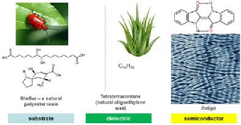
"Green electronics" represents an emerging research area, within the field of organic electronics, aimed at exploiting the potentiality of natural compounds and their derivatives as functional materials for innovative, low-cost and sustainable electronic devices (Figure 1).
Figure 1: Example of materials set for a nature-inspired organic field effect transistor
Main goals of “green electronics” are: 1) the considerable reduction of the cost of production of the devices by using highly abundant and low cost bio-materials; 2) the fabrication of efficient bio-degradable materials for more sustainable electrical devices; 3) the increase of the bio-compatibility of the devices for a more efficient integration in human, animal and plant tissues (Figure 2).
Figure 2: a) Skin integrated device for physiological measurements and stimulation; b) Electronic rose: plant integrated device for physiology regulation, energy harvesting from photosynthesis, and plant optimization
beyond genetic modifications.
Starting from this background, the research activity of my PhD has been aimed at the design, synthesis, characterization of the opto-electronic properties and processing of natural and/or Nature-inspired materials for organic light emitting diodes (OLEDs).
6
OLED devices, this approach may be largely rewarded by the demonstrated opportunity of processing flexible ITO-free devices by using the most attractive printing technology for roll-to-roll large area manufacturing.
In a second set of very preliminary experiments, the potential of PLA (polylactic acid) as innovative biodegradable substrate for OLED devices was tested for the first time. Also in this case there are some problems that need to be overcome, such as the sensibility of PLA to the high temperatures and to many common organic solvents; further experiments are still in due course.
2) Synthesis and electrical properties of eumelanin thin films: towards the design of polymeric anode for ITO-free devices
This section has been developed within the frame of a research line aimed at testing the potential of eumelanins, the brown-black pigments that hold important functions in human body, as materials for organic electronics devices.
a) Analysis of factors governing the solid state polymerization process
The ammonia induced solid state polymerization (AISSP) is an innovative technique allowing the deposition of quite homogeneous melanin thin films on different kind of substrates.
Herein is reported a study aimed at assessing the role of temperature, oxygen and water in the solid state polymerization process of 5,6-dihydroxyindole (DHI), the monomer melanin precursor.
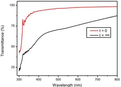
To this aim the process was studied by following the evolution of the transmission spectrum over the time under different ambient conditions.
Since the polymerization process consists in a series of oxidative reactions, the oxygen flux is fundamental for the determination of the process rate; water and temperature further accelerate the oxidation.
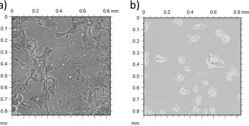
In another set of experiments it was also evaluated how the ambient conditions can influence the morphology of the melanin thin film. Eumelanin thin films obtained at higher temperatures and oxygen flows show higher roughness and heterogeneity. On the contrary, although water can accelerate the oxidative process leading to melanin thin films, it is also able to give a surface solubilization effect of the material with a consequent smoothing and homogenizing effect.
b) Study on the electric conductivity of eumelanin thin films
The electrical characteristics of eumelanin thin films realized by ammonia induced solid state polymerization (AISSP) were also studied. Both monomers, DHI (5,6-dihydroxyindole) and DHICA (5,6-dihydroxyindole-2-carboxylic acid) were used in the thin film fabrication to evaluate the effect of the chemical composition on the electrical property of the material.
In the first set of experiments, the current-voltage measurements of a device fabricated by using eumelanin thin films as semiconductors among two planar platinum electrodes
7
were performed. The work was carried out in association with Prof. Clara Santato at the Polytechnique of Montreal (CA) (from 01/09/2016 to 23/12/2016).
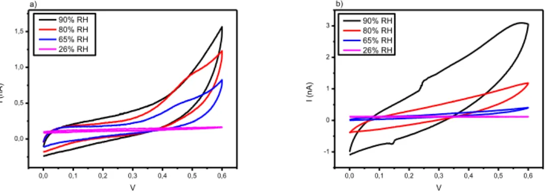
In the second set of experiments, the electronic and protonic current of eumelanin materials was evaluated by using Pd and PdHx electrodes under different humidity conditions.
The experimental results confirm the capability of the eumelanin materials to act as hybrid ionic-electronic conductors under humidity conditions. The presence of traps, the morphology and the chemical composition further influence the electric properties as observed for most of the disorder organic materials. The right synergy between morphology, chemical composition and electric properties is still an open issue for the researchers.
3) Synthesis of Nature-inspired organic electroluminescent materials for the emitting layer in OLED applications
This section has been aimed at the design and the synthesis of a series of Nature-inspired electroluminescent complexes for OLED applications.
a) Synthesis of electroluminescent dopamine-inspired iridium(III) complexes
In this work the attention was focused on the synthesis and characterization of new dopamine-inspired iridium(III) complexes as electroluminescent materials for organic light emitting diodes (OLEDs). In particular a set of new iridium(III) complexes was prepared, namely a series of 1-phenyl-6,7-dimethoxy-3,4-dihydroisoquinoline (PHQ) derivatives (Figure 4).
OLEDs based on phosphorescent transition-metal complexes are attracting great attention since they can improve electroluminescence performances as compared with the conventional fluorescent OLEDs. According to spin statistics, electroluminescence from fluorescent molecules can reach a maximum quantum yield of 25%, but in phosphorescent complexes it can theoretically achieve quantum yields up to 100%, since both triplet and singlet excitons can be harvested for the emission. Among all the phosphors, cyclometalated iridium(III) complexes are acquiring a mainstream position in the field of organic displays because of their highly efficient emission properties, relatively short excited state lifetime and excellent colour tunability over the entire visible spectrum.
For the synthesis of PHQ ligands a similar procedure was followed. This consisted in the reaction of the selected benzoic acid with ethylchloroformate and O,O-dimethyldopamine to form the intermediate amide derivative, followed by the intramolecular cyclization with POCl3 to give the desired compounds (Figure 4).
R COOH NH2 MeO MeO N H O R MeO MeO N R MeO MeO 1. Ethylchloroformate, TEA, DMF, 0° C, Ar 2. 60° C, Ar R = H Benzoic acid R = F 4-Fluorobenzoic acid R = OMe 4-methoxybenzoic acid R = CN 4-Cyanobenzoic acid Am_1 (98%) Am_2 (91%) Am_3 (97%) Am_4 (92%) POCl3 EtOH:DCM 3:11 130° C PHQ (95%) PHQ_F (76%) PHQ_OMe (70%) PHQ_CN (66%)
8
For the synthesis of the iridium(III) complexes a procedure based on the intermediate formation of a chloro-bridged dinuclear complex (μ-Ir) with the initial insertion of 2-phenylpyridine (ppy) was followed.
N IrCl3 N Ir N Ir N Cl Cl N 2-Phenylpyridine H2O/EtOEtOH, reflux, 18h Ar Atm -Ir (72%)
Figure 5: Synthesis of the dichloro-bridged dinuclear complex (μ-Ir)
According to a procedure reported in the literature, the intermediate μ-Ir was treated with a molar excess of the proper PHQ ligand in presence of acetylacetone and TEA in DMF under reflux conditions. This procedure provided one-pot the synthesis of three different neutral iridium(III) complexes of general formula Ir(ppy)x(PHQ)y differing for the
ratio between the ppy and PHQ units (Figure 6).
9
All the synthesized compounds were fully characterized by 1H and 13C NMR analysis confirming the structures. 19F NMR spectroscopy was also used to confirm that the fac isomers of the homoleptic iridium complexes tri-substituted with PHQ-type ligands were formed.
The photo-physical properties of the iridium complexes were investigated in diluted solutions in DCM. It is possible to note that parameters such as the structure of the complex and the nature of the substituents on the phenyl ring induced shifts of both the absorption and emission maxima.
OLED devices were fabricated with the synthesized iridium(III) complexes used as guests at different percentages (2%, 6% and 12% w/w) in the 4,4'-bis(N-carbazolyl)-1,1'-biphenyl (CBP), selected as the host. The selected OLED configuration was the following: ITO/PEDOT:PSS/Ir:CBP/BCP/Alq3/Ca/Ag.
All the fabricated devices exhibited a red electroluminescence with significative shift of the emission maximum observed by changing the nature of the substituents on the phenyl ring of the iridium complexes.
The best devices in terms of luminance and turn-on voltage resulted those prepared by using a 2% wt of the iridium(III) complexe, reaching maximum luminances of 1092 cd/m2 and 2474 cd/m2.
b) Synthesis of transition metal complexes with natural β-diketones
In this section the potential of curcumin (1) and 6-dehydrogingerdione (2), two naturally occurring β-diketones, as ligands in transition metal complexes, such as Ir(III) and Zn(II) complexes, were tested.
Well known for their antioxidant, anti-inflammatory and anticancer properties, curcumin is obtained from the rhizome of Curcuma longa and is the main component of turmeric, and 6-dehydrogingerdione is obtained from the rhizome of Zingiber officinale and is the main component of ginger.
The use of the easily accessible zinc(II) in addition to iridium(III) is a deliberate choice towards a green approach to OLED fabrication.
Both ligands and the corresponding transition metal complexes were synthesized in good yields and on large scale, and were subjected to spectroscopic characterization. A comparative investigation of their photo-physical properties were carried out both in dilute solutions and on thin films by UV-visible and emission spectroscopy: all the complexes exhibited a green emission (from 480 to 524 nm) and quantum efficiencies up to 1.7% for iridium complexes and up to 78% for zinc complexes.
The iridium and zinc complexes synthesized by using nature-inspired β-diketone ligands, respectively curcumin and 6-dehydrogingerdione showed photoluminescence in the green region.
OLED devices realized with the iridium complexes showed limited performance due to aggregation phenomena in thin film. Zinc complexes show very poor solubility in the common used organic solvents. They were tested as fluorescent emitters in a standard device structure (ITO/PEDOT:PSS/Zn complex/BCP/Alq3/Ca/Ag). Deposition of the zinc complexes were performed from solution (dimethyl sulfoxide) and with a thermal vacuum deposition, unfortunately in both cases, although devices show a diode electrical
10
behavior, the emission of the zinc complexes was not observed. As future development, the synthesized zinc complexes can be structural modified to improve the solubility and/or they can be tested as host and/or electron transport material.
These data pointed out the potentiality of these new nature-based complexes as organic materials for optoelectronic application and represent the good starting point toward the development of more sustainable OLED devices.
4) Synthesis and processing techniques of biocompatible and low cost materials for encapsulating layers in OLED devices
In the last section of the thesis, low-cost encapsulation methods for flexible OLED devices have been studied. The permeation process is a very complex phenomena and different mechanisms are involved. As a consequence, different approaches can be used to realize a barrier layer.
The use of oxides materials is one of the most used solution for the realization of high performances barrier layers by using vacuum deposition techniques. On the contrary, vacuum techniques are expensive and often very slow.
In this work ceramic, hydrophobic and water absorbing thin film were realized to test the possibility to realize a barrier multilayer for electronic devices.
ZnO nanoparticles deposited by solution based processes were used as an alternative to inorganic barrier films realized by vacuum techniques. The obtained ceramic thin film showed different permeation mechanisms in relation to the used deposition technique and to its microstructure. The impossibility to use high temperatures to proceed with sintering process is the main obstacle to further improve the barrier properties.
An “active” multilayer approach is proposed to reduce the water permeability of the solution-based ZnO layer; in particular, the adsorption phase of the permeation process can be slow down by reducing the surface interactions between the penetrant and the barrier materials. Hydrophobic and/or oleophobic treatments of surface reduce its wettability and slow down the adsorption process.
Hydrophobic layers were prepared by using functionalized ZnO nanoparticles with stearic acid deposited on PEN substrates. An improvement of the barrier properties with respect to the only ZnO nanoparticles layer was observed and it was demonstrated how the hydrophobicity is capable to slow down the permeation process and improve the multilayer barrier performances. It was also demonstrated that it is possible to merge the use of a ceramic and hydrophobic material in a single step deposition process.
Moreover, a water absorbing interlayer can be introduce for further improve barrier performances and a hydrogel thin film was realized to test this hypothesis.
It is reported that a double layer hydrogel/ZnO nanoparticles shows better barrier properties with respect to the sole ZnO nanoparticles layer and comparable performances with the hydrophobic layers.
Although the hydrophobic and the hydrogel layers act according to different mechanisms, both solutions can be exploited to improve the ceramic layer barrier properties.
Different functional thin film were realized by using solution based deposition techniques, demonstrating how is possible to easily confer the desired characteristics to a layer. The
11
proposed methods can be used for preparing multilayer structures that can be very attractive for packaging applications and encapsulation of moisture sensitive devices.
12
~INTRODUCTION~
In our lives we are constantly surrounded by electronic devices and it is impossible to imagine ourselves without using such devices. The market demand for electronic devices is growing every day from both the points of view of the quantity and the performances. In this context, inorganic semiconductors remain fundamentals. Nevertheless, at present, the energy efficiency of these devices is not able to balance the economic and energy costs needed in the production phase.1 Furthermore, the huge demand of electronics is leading to a massive amount of electronic waste and to a great demand of rare elements such as gallium and indium.2
From these premises, the use of organic semiconductors and materials to prepare electronic devices can be seen as an answer to the problems posed by the inorganic counterparts. The interest in what is currently called "organic electronics" was born with the discovery of the electrical conduction properties of some organic materials. The first organic conductive material (polyaniline) was reported by Henry Letheby in 1862 by anodic oxidation of aniline in sulfuric acid.3 Successfully, in 1954, high conductivity of 0.12 S/cm was reported in perylene-iodine complex.4
In 1977, Shirakawa et al. reported the high electrical conductivity of iodine-doped polyacetylene5 a research that was awarded in 2000 with the Nobel prize in Chemistry for "The discovery and development of conduction polymers". In the same period, highly conductive polypyrrole was also discovered.6 These kind of materials led to a huge interest in organic electronics.
In the early stages, the term “organic” was referred to the typology of semiconductor materials employed in this new kind of devices; with the evolution of the technology, the term “organic” has acquired a wider meaning referring also
13
to the other materials than constitute the electronic devices such as dielectrics, substrates, etc.
Nowadays, when we talk about organic electronics we refer to that set of technologies and materials that allow us to obtain light and flexible devices with the possibility of realizing them on large areas thanks to the peculiar mechanical properties of the organic materials.7 With organic materials it is indeed possible to use easy and low cost solution-based processing techniques such as printing techniques.8 Another advantage of the organic materials is the possibility of tuning their properties at molecular level, to modulate the characteristics and performances in a detailed way to meet the devices requirements. Organic materials can be tailored: for example by varying functional groups and/or the polymer length with the aim of changing the band gap and allowing the electronic tunability.9
On the other hand, poor crystallinity, low mobility and degradation susceptibility of organic materials represent today the greatest obstacles to the commercialization of organic devices.
Among organic electronic devices, organic light emitting diodes (OLEDs), organic photovoltaics (OPVs) and organic field-effect transistors (OFETs) are the most known.
An OLED mainly consists of an electroluminescent organic material sandwiched between two electrodes (Figure 1).
14
Figure 1: Structure organic light emitting diode
OLED devices find application in different fields from civil lighting to electronics, from automotive industry to biomedical devices, from interior design to light art and fashion industry. Now mobile telephones and laptop displays, TV sets and design lamps based on the OLED technologies are largely diffused on the market (Figure 2).
15
An organic solar cell or plastic solar cell is a type of photovoltaic device that uses organic materials for light absorption and charge transport to produce electricity from sunlightexploiting the photovoltaic effect.10
A typical OPV device consists of one or several photoactive materials sandwiched between two electrodes (Figure 3). The molecules most commonly used in organic solar cells are solution-processable, as they are cheap allow high throughput, resulting in low production costs to fabricate potentially cost-effective large volume photovoltaic devices. The optical absorption coefficient of organic molecules is high, so a large amount of light can be absorbed with a small thickness of the materials (usually on the order of hundreds of nanometers). The main disadvantages associated with organic photovoltaic cells are the low efficiency, low stability and low strength compared to inorganic photovoltaic cells such as silicon solar cells. Polymer solar cells, as other organic electronic devices, can be lightweight, potentially disposable and flexible, and customizable at the molecular level. Polymer solar cells also have the potential to exhibit transparency, suggesting applications in smart windows, walls, flexible electronics, etc. The disadvantages of the polymer solar cells are also serious: they offer about 1/3 of the efficiency of the hard materials, and experience substantial photochemical degradation.11 As a result, polymer solar cells efficiency and stability problems are the main topics in the solar cell research.
16
Figure 3: Structure organic solar cell
An organic field effect transistor is realized with a layered structural design consisting of a thin film of organic semiconductor, an insulator, and three electrodes named source (S), drain (D), and gate(G) as shown in Figure 4. The source and drain electrodes inject and extract the charge carriers, respectively, and are in contact with the active layer. On the other hand, the gate is separated from the semiconductor film by the insulator. The voltage applied to the gate controls the conductivity of the semiconductor between source and drain (channel). The channel in a transistor is formed by the accumulation of the charge in the semiconductor.12 The field-effect transistor was first proposed by J.E. Lilienfeld, who received a patent for his idea in 1930.13 He discovered that a field-effect transistor behaves as a capacitor with a conducting channel between a source and a drain electrode. Applied voltage on the gate electrode controls the amount of charge carriers flowing through the system. The first field-effect transistor was designed and prepared in 1960 by Kahng and Atalla using a metal-oxide-semiconductor structure (MOSFET).14 As previously mentioned, the rising of the materials and manufacturing costs and the interest in the use of more
17
environmentally friendly electronic materials have supported the development of organic electronic devices, and in 1987 Koezuka and co-workers reported the first organic field-effect transistor based on a conjugated polymer of thiophene molecules.15
Many OFETs are now designed based on the thin-film transistor (TFT) model, which allows the devices to use less materials.
OTFTs are the fundamental unit for basic circuits and are now widely used in active matrix displays, RFID (Radio-Frequency IDentification) tags, sensors and actuators conditioning.
Figure 4: Structure of organic field effect transistor
The lighting evolution
With the discovery of fire, people had the possibility to illuminate an area, firstly with campfire or torches and thanks to the technological evolution with oil lamps and candles. With the advent of electricity, electric lighting became predominant. The first electric light was created by Humphry Davey in the first decade of 1800; he realized the first incandescent light using a bank of batteries and two charcoal roads (arc light).
In 1879 Thomas Edison invented a long-lasting electric light bulb that could compete with gas lighting. In particular with a carbonized bamboo filament was possible to have light for 1200 hours. Incandescent bulbs would go on to dominate the world of lighting until fluorescent lights were commercially introduced by Daniel McFarlan Moore in 1904. Although fluorescent light required
18
high voltage and non-standard connectors to operate, their higher efficiency, compared to incandescent lights, led the major incandescent manufacturer General Electric to improve upon their incandescent technology by introducing the tungsten filament. The 20th century was the century of high density discharge (HID) lamps. The most popular types of HID lamps are the fluorescent, the mercury-vapor, the high-pressure sodium, and the metal-halide lamps. All of these lamps exploit a technology based on a visible light generated via an electrical current between two metal electrodes through a glass tube filled with inert gas. The lighting technology change substantially with the birth of the solid state lighting (SSL) era. In this emerging concept for illumination, selected semiconducting materials can produce visible light under the action of an electrical field (electroluminescence) in suitably engineered devices where the transport of charge occurs in one specific direction (diodes). Through this approach, the primary product of these lighting devices is the photon itself, unlike traditional sources where visible light is essentially a by-product of other processes, such as heating or discharging. As a result, SSL produces visible light with reduced heat generation and energy dissipation, while its solid-state nature provides greater resistance and lifetime, with limited impact on the environment. First examples of SSL devices are LEDs (Light Emitting Diodes), an inorganic-based semiconductor device that emits visible light of a defined color when a voltage is applied. The first LED was invented in the 1960 by General Electric scientist Nick Holonyak. From 1960 to nowadays, LED technology has evolved in terms of emission spectra, cost and efficiency so that now such technology represent the undisputed leader in lighting industry.
Thanks to the discovery of the semiconducting and electroluminescence properties of organic materials,16 in the last 30 years the Organic Light Emitting
19
Diode (OLED) technology was introduced as possible alternative to LED technology.
Figure 5: Technology evolution of the lighting
Fluorescence and Phosphorescence
Typically, organic molecules in their ground state have paired electrons in all the orbitals, thus a total spin equal to zero gives a singlet state (S0). Upon the
absorption of an incident radiation of a given energy, an electron from the outer orbital can be promoted to an unoccupied high energy orbital leading the molecule to an excited state (Sn).
Within the Sn states, there are several energy levels. The bigger gap between the
second and first excited state is overcome by internal conversion (IC) and during this conversion the spin of electrons is maintained (Figure 6). After that, the electrons can relax vibrationally until they reach the lowest energy level of the S1
state. The electrons could relax even further in a non-radiative way until they eventually reach the ground state again, but it can be the case that the last amount of energy is too large to be released to the surroundings, because the surrounding molecules cannot absorb this much energy. In this case, fluorescence occurs with emission of photons of a specific wavelength.
21
Figure 7: Jablonski diagram
OLED devices
An organic light emitting diode (OLED) is an optoelectronic device in which an organic electroluminescent material is sandwiched between two electrodes, with at least one of the two contacts being transparent to allow light emission. The physical process is based on the electroluminescence (EL). With voltage application, anode and cathode inject respectively holes and electrons that move through the layers and recombine in the emitting layer with exciton formation. Relaxation of the exciton produce light emission (electroluminescence) with a wavelength strictly dependent on the electronic properties of the emitting material.
High photo-luminescence is a necessary but not sufficient condition for electroluminescence.
In the simplest version, an OLED device is composed of a single organic emitting layer between an anode and a cathode (monolayer device); since the HOMO and LUMO of the emitting layer, in the most of the cases, are set at energy levels very different from those of the two electrodes, organic multilayer structures have
22
been developed in order to improve the device performances. This can help holes and electrons movements supporting the recombination in the emissive layer. A typical multilayer structure is composed by: anode, HIL (hole injection layer), HTL (hole transport layer), EML (emitting layer), ETL (electron transport layer), EIL (electron injection layer) and cathode as reported in Figure 8, and it can be designed to perfectly balance charge injection and transport with the aim of optimizing the recombination process.
Figure 8: OLED multilayer structure
The anode component typically used is indium tin oxide (ITO). This material is transparent to visible light, it show good electrical conductivity (~104 S/cm) and it has a high work function which promotes injection of holes into the HOMO level of the organic layers. Due to the high costs and the limited availability of indium, the fragility and lack of flexibility of the indium-tin oxide layers, and the high costs of deposition techniques that require high temperatures and sometimes high vacuum levels, researcher are working on alternative anode materials.
A typical conductive layer behaving as a transparent electrode that replace the traditionally used ITO is PEDOT:PSS , a blend of the two polymers
poly(3,4-23
ethylenedioxythiophene and poly(styrenesulfonate) (Figure 9).17 PEDOT:PSS is a transparent and conductive blend (>200 S/cm) with high flexibility, and since its HOMO level lies between the work function of ITO and the HOMO of other commonly used polymers, it is able to reduce the energy barriers for hole injection.
Figure 9: PEDOT:PSS structure
The hole injection layer (HIL) improves the electrical properties of the device and it is able to smooth the ITO surface.18 A typical HIL is constituted by PEDOT:PSS. The electron transport layer (ETL) and/or the electron injection layer (EIL) are necessary to help electrons injection and transport from the cathode layer. Typical electron transport materials are: tris-(8-hydroxyquinoline)aluminum (Alq3),
3-(Biphenyl-4-yl)-5-(4-terz-butylphenyl)-4-phenyl-4H-1,2,4-triazole (TAZ) and 2,2′,2"-(1,3,5-Benzinetriyl)-tris(1-phenyl-1-H-benzimidazole) (TPBi) (Figure 10).19
24
Figure 10: Electron transport materials
Both hole and electron blocking layers are used to confine charges. Typical hole and electron blocking materials are bathocuproine (BCP) and tris(4-carbazoyl-9-ylphenyl)amine (TcTa) respectively (Figure 11).20,21
Figure 11: Hole and electron transport materials
Of course, all materials of the multilayer structure must be chosen to reduce charge injection barriers.
The cathode component depends on the type of OLED required. Noteworthy, even a transparent cathode can be used. Usually metals like barium, calcium and aluminum are used as cathodes because they have work functions lower than anodes, which helps in injecting electrons into the LUMO level of the different layers.22
25
The emitting layer is the main component of an OLED device and it is constituted by an electroluminescent material. This can be a small molecule, a transition metal complex and a polymer.
Small molecules such us pentaphenylcyclopentadiene and transition metal complexes involving zinc, beryllium, copper and barium have been widely used as emitting layer in small molecules organic light emitting diode devices (SM-OLED) (Figure 12).23 Devices prepared with such materials result in moderately low bias voltages and attractive luminance efficiency. Fluorescent small molecules can be easily synthesized and designed to obtain all the primary colors. The production of small molecule devices and display usually involves thermal evaporation in a vacuum, since insolubility of this kind of materials. This makes the production process more expensive and of limited use for large area devices, than other processing techniques. Nevertheless, vacuum deposition enables the construction of very complex multi layer structures to optimize devices performances.
Figure 12: Small molecules used as emitting materials
Fluorescent conjugated polymers represent the ideal candidate for commercial applications. Polymer OLED (P-OLED) 24 materials do not perform as good as
SM-26
OLED in terms of lifetime and efficiency. This can be explained considering that they have higher hole conductivity than electron conductivity and so excitons form usually close to the cathode and often tend to relax non radiatively via energy transfer.
Anyway, devices based on this kind of polymer exhibit efficiencies around 20 lm/W, close to those of inorganic LEDs. Polymers are soluble and available as inks for printable electronics applications, they show good flexibility and it is usually required a relatively small quantity of material for large area deposition so they are more suitable for the realization of large-screen displays. On the contrary, it is not possible to realize complex multilayer structures since with solution based deposition process there are problem of compatibility between solvents used for deposition and materials already deposited to realize the device (perpendicularity); this is another reason why P-OLED devices show limited efficiency. Typical polymers backbones used include derivates of poly(p-phenylene vinylene) and polyfluorene (Figure 13). This kind of materials offer many opportunities for the control of electronic, chemical, morphological and rheological properties. Substitution of side chains onto the polymer backbone or variation of the backbone structure may determine the stability and solubility of the polymer and the color of emitted light.
Figure 13: Polymeric backbone used as emitting materials in P-OLED
In order to improve the performances and the brightness of the devices, OLED based on phosphorescent emitting molecules25 (PH-OLEDs) are becoming predominant.
27
Phosphorescent organic light emitting diodes use the principle of electro-phosphorescence to convert electrical energy into light in a highly efficient manner.26
According to spin statistics, in PH-OLED all the four different combinations of excited states are possible, one combination of antiparallel spin giving a singlet (accounting for the 25% of excitons), and three combinations of parallel spin giving a triplet (accounting for the 75% of excitons)27 so by harvesting both singlet and triplet excitons, PH-OLEDs overcame the limit of SM-OLEDs due to low efficiencies, approaching a theoretical internal quantum efficiency of 100%.
Efficient phosphorescence is rare at room temperature, and few materials emit efficiently in homogenous films due to the quenching effects by surrounding molecules. The solution to these demands is found by doping the luminescent material into a charge transport host material.28 Emission then occurs by direct carrier trapping and exciton formation on the luminescent dye, or by exciton formation in the host and energy transfer to the luminescent guest.
The energy transfer mechanism is not completely clear and understood. Two mechanisms are possible: the Dexter transfer and the Förster transfer (Figure 14).29 The Dexter electron transfer is a fluorescence quenching mechanism in which an excited electron is transferred from one molecule (a donor) to a second molecule (an acceptor) due to hopping of the electrons. The process requires an overlap of the wavefunctions between the donor and the acceptor, which means it can only occur at short distances (typically within 10 Å). The excited state may be exchanged in a single step, or in two separate charge exchange steps.
In the Föster mechanism (FRET), transfer occur through non radiative dipole-dipole coupling. The efficiency of this energy transfer is inversely proportional to the sixth power of the distance between donor and acceptor, so this process is
28
extremely sensitive to small changes in the distance. FRET occurs over large distance as compared to Dexter energy transfer (10-100 Å).
Figure 14: Energy transfer mechanisms in host-guest systems
Device fabrication
Deposition techniques are a fundamental aspect in the organic electronic device fabrication.
Inorganic and metallic materials are deposited usually by e-beam, sputtering, thermal deposition, ecc.
Organic semiconductors can be deposited either from vapor or solution phase, depending on their vapor pressure and solubility. Of course, device performances are greatly influenced by the deposition conditions, that influence the resulting molecular structure and the morphology of the thin film.30
Vacuum thermal evaporation is a process that consist in the heating of the organic semiconductor using a resistive heating source under a pressure in the range of 10-8 to 10-6 torr (Figure 15). Organic small molecules and oligomers are usually deposited by vacuum thermal evaporation due to their insolubility. By using
29
vacuum thermal evaporation it is possible to obtain with a good reproducibility films with high uniformity. Multilayer deposition and co-deposition of several organic semiconductors are possible without the concerns of delamination and/or dissolution of the previous layers during subsequent deposition steps. On the other hand, vacuum techniques are time expensive and require a relatively high amount of material, without considering the initial cost for the equipment setup. Furthermore, there is a limitation in the dimensions of the device due to the relatively small dimensions of the vacuum deposition chamber.
Figure 15: Vacuum thermal evaporation chamber
Solution based deposition techniques show few advantages such as: they are not limited by the size of the vacuum chamber, no pumping down time is required, low cost of production.
Both spin coating and solution casting are commonly used for solution deposition. In the spin coating process, a liquid precursor or a solid dissolved in a proper solvent is deposited on a smooth and flat substrate which is subsequently spun at a high rate to centrifugally spread the solution over the substrate. The desired thickness can be reached by acting on the speeding rate, the time of spinning and by performing repeated deposition. In the spin coating method, the solvent dries
30
relatively fast allowing less time for molecular ordering, as a consequence an annealing treatment is often carried out in order to crystallize the amorphous spin coated film. Dip coating is another solution deposition technique, in this case the substrate is completely submerged in the solution and then withdrawn under controlled conditions. By controlling the withdrawal speed, the evaporation conditions (i.e. humidity, temperature) and the volatility and viscosity of the solvent, the film thickness, homogeneity and morphology can be controlled. Since the evaporation of the solvent is slower than in the spin coating process, with dip coating it is possible to obtain a good molecular order , although the film uniformity is usually better for spin-coated films.
The Langmuir-Blodgett (LB) technique is another possible solution method to deposit organic thin films. LB film consists in an ordered array of amphiphilic molecules deposited from the surface of a liquid onto a solid by immersing the solid substrate into (or from) the liquid. The molecules in the LB film are usually well-aligned.
a) b) c)
Figure 16: a) spin coating deposition; b) dip coating deposition; c) Lanmuir-Blodgett deposition
In the device fabrication it is not only important the thin film deposition process but also the patterning of both conductor and semiconductor layers. The distances and the specific overlap between different layers and materials need to be specifically designed in order to reach the best device performances. As in all the steps of the fabrication process, cost, achievable feature size and materials
31
compatibility need to be considered. There are three main types of patterning procedures: optical lithography,31 shadow masking32 and printing.33
Optical lithography or photolithography is a conventional technique for patterning and realization of components for microelectronics and photonic devices (Figure 17). This technique is based on the deposition of a photoresist layer that is subsequently exposed to UV light through a mask. UV light exposition induces chemical changes in the exposed regions making the photoresist more soluble (positive resist) or less soluble (negative photoresist) in a specific solution. The soluble portion is so removed leaving a photoresist pattern. If the resist is deposited directly on the layer that is necessary to pattern, the patterning is followed by an etching process of the region not covered with photoresist. The subsequent removal of photoresist residues leave a patterned layer. This kind of process is called direct photolithography and is very used in the field of the organic electronic devices for the pattern of the ITO layer. Another photolithographic technique consists in the deposition of the thin film on top of a patterned photoresist layer and subsequent dissolution of the photoresist, leaving a pattern of the substrate of the deposited material (lift-off).
32
Photolithography generally has relatively high cost per unit area, the substrate size is limited by the size of the exposure tools and the resolution is around 80 nm, for such reasons this technique is usually used for realization of high added value components.
Materials can also be patterned directly in the deposition phase by using a shadow mask. Shadow mask is often used in the vacuum thermal evaporation process. The device size is limited by the size of the mask and the resolution is around 25-40 m.
Driven by the necessity to have low cost, large area and flexible devices, significant progress has been made by printing methods. The main printing techniques used for device fabrication are: ink jet printing, screen printing, flexography and gravure printing (Figure 18).
Ink jet printing consists in the deposition of liquid droplets on a substrate with a specific pattern that can be easily changed. Since inkjet deposits material by jetting droplets from a nozzle that is scanned relative to the substrate, in order to achieve high throughput, a large number of nozzles must be used, which increases the risk of nozzle clogging. Furthermore, minimum feature size is limited by the nozzle size and drop placement accuracy especially at high print speeds. Thus, non-digital printing methods such as screen printing, flexography and gravure are more promising for scaled-up of the devices manufacturing.
In the screen printing, a specially formulated ink is squeezed through a screen mask onto the substrate surface to form a desired pattern. Screen printing requires inks with high viscosity and so it is ideally suitable for thick films deposition. The limitation with screen printing is the feature size it can print: 75 m is the smallest feature size that is reproducible unless surface patterning is used, so that the printed ink does not spread.
33
Both flexography and gravure printing use a roll that is inked, from which patterned ink is transferred to the substrate. They differ in how the pattern is created on the roll. In flexography the pattern consists of raised features that are inked from an anilox roller. The resolution of flexography is limited by the low stiffness of the material from which the patterned roll is fabricated. Gravure is most promising in terms of resolution and print speed. In gravure printing the pattern is made up of recessed cells below the roll surface. These cells are filled with ink and excess ink is removed from the land areas in between the cells using a doctor blade. Gravure cylinders are typically made from metals such as copper with a chromium coating. This results in excellent dimensional stability, roll durability and pattern fidelity and also compatibility with a wide range of solvents.
a) b) c) d)
34
~AIMS OF THE THESIS WORK~
What discussed till this point represents the background from which I have started my PhD work that has been focused on synthesis, optoelectronic properties and processing of bio-inspired soft materials: toward new «green» electronic devices. "Green electronics" represents an emerging research area, within the field of organic electronics, aimed at exploiting the potentiality of natural compounds and their derivatives as functional materials for innovative, low-cost and sustainable electronic devices.34
Main goals of “green electronics” are: 1) the considerable reduction of the cost of production of the devices by using highly abundant and low cost bio-materials; 2) the fabrication of efficient bio-degradable materials for more sustainable electrical devices; 3) the increase of the bio-compatibility of the devices for a more efficient integration in human, animal and plant tissues.
All the different components of an electronic device can be thought in a "green" electronic vision, from the substrate to the encapsulating layer, from the electrode to the semiconductor (Figure 19).
35
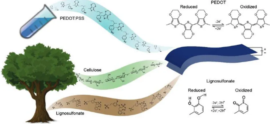
Different natural and synthetic biodegradable and biocompatible substrates have been successfully used for electronic devices. Paper is employed in devices for storage, generation and harvesting of energy35,36 and recently it was demonstrated that the performances of an all-organic paper supercapacitor based on nanocellulose and PEDOT:PSS is enhanced by incorporating lignin, another abundant and natural biopolymer (Figure 20).37
Figure 20: Schematic of the paper supercapacitor with the molecular structures of its constituents
PDMS (polydimethylsiloxane), PVA (polyvinyl alcohol) and PLA (polylactic acid) are examples of biocompatible synthetic polymers used as substrate in electronic devices (Figure 21).38,39,40
36
Fully biocompatible and biodegradable substrates are also of great interest. Silk was employed as a platform for the fabrication of sensing devices for the food industry.41
Recently, also inorganic scaffolds have been used such as biosilica from living diatoms used in photonics and electronics (Figure 22)42 and the carbonate microstructures from sand dollars converted into perovskite semiconductors (Figure 23).43
Figure 22: Scanning electron microscopy images of a Thaòassiosira weissflogii frustules: a) after soft acid treatment the whole structure is preserved; (b,c) after hard acidic oxidative treatmment, theintricate
pattern of pores in clearly visible. Markers: (a) 1 μm; (b) 100 nm; (c) 200 nm
37
The "green" electronics developed parallely with bio-electronics because the biocompatibility and the biodegradability are requirements for electronic devices to be interfaced with biological systems.
OFETs (organic field effect transistors) were used as selective sensors by incorporating receptors molecules. The receptors are able to selectively bind analytes of interest with a modification of the electric signal of the device.44
The group of Prof. Malliaras reported on the use of an EOCT (Organic electrochemical transistor) device for in vivo recording of brain activity in rats.45 The group of Prof. Rolandi realized for the first time an OFET based on proton charge transport by using maleic-chitosan proton conducting layer as semiconducting material and PdHx as proton conductors.46
An important contribution was given by the group of Prof. Berggren with the introduction of two innovative devices that can be used as logic gates and delivery systems, respectively the ion bipolar junction transistors (IBJTs) and the organic
electronic ion pumps (OEIPs) (Figure 24).47
Figure 24: device structures of a) ion bipolar junction transistors (IBJTs); b) organic electronic ion pumps
(OEIPs)
In particular, ion pumps were successfully used in vitro, in vivo and in plantae with few examples reported in Figure 25.48
38
Figure 25: Application of ionotronic devices: a)affectring auditory responde in guinea pigs in vivo; b) Regulation growth rate in plants by controlled delivery of a plant hormone gradient
With its electronic rose prof. Berggren demonstrates for the first time the integration of a plants "circuitry" with electronics and how this can lead to a selective control of plant physiology (Figure 26).49
Figure 26: Electronic rose, plant integrated device for physiology regulation, energy harvesting from photosynthesis, and plant optimization beyond genetic modifications.
In this scenario is set my work that has been aimed at the design of a "green" OLED device.
In particular I focused the attention on four main components of the device: 1) the substrate; 2) the anode; 3) the emitting layer; 4) the encapsulating layer (Figure 27).
The research activity has been reported in the following four sections:
SECTION 1- processing techniques for the fabrication of ITO-free substrate based on the standard PEN and the biodegradable PLA for flexible OLED devices;
40
REFERENCES
1 E.D. William et al, IEEE Int. Symp. Electr. Environ., 2004, 0-7803-8250-1/04 2 B.C.J. Zoeteman et al, Int. J. Adv. Manuf. Technol., 2010, 47, 415-436 3 H. Letheby, J. Chem. Soc., 1862, 15, 161–163
4 H. Akamatu et al, Nature, 1954, 173, 168
5 H. Shirakawa et al, J.C.S. CHEM. COMM., 1977, 16, 578 6Dall’olio et al, CR Acad. Sci. Paris, 1968, 267, 433–435 7 A.C. Arias et al, Chem. Rev., 2010, 110, 3-24
8 M. Berggren et al, Nature Materials, 2007, 6, 3-5 9 J. Rivnay et al, Chem. Mater., 2014, 26, 679-685 10 D. Wöhrle et al, Adv. Mater., 1991, 3, 129-138 11 Q. L. Song et al, Appl. Phys. Lett., 2006, 89, 251118 12
G. Horowitx , Adv. Mater., 1998, 10, 365-377
13
J.E. Lilienfeld, US 1745175(1930) "Method and apparatus for controlling electric currents"
14
J. Atalla and D. Kahnq, US 3102320 (1963) "Metal Oxide Semiconductor (MOS) Transistor"
15 H. Koezuka et al, Synthetic Metals, 1987, 18, 699-704 16 A. Bernanose et al, J. Chim. Phys., 1953, 50: 64
17 S. A. Carter et al, Appl. Phys. Lett., 1997, 70, 2067-2069
18 T.-C. Li et al, Int. Journal of Precision Engineering and manufacturing-Green
Technology, 2014, 1, 4, 329-334
19 Y. Karzazi, J. Mater. Environ. Sci., 2014, 5, 1-12 20
A. Uniyal et al, "Improvement in Performance of OLED by introducing additional
hole blocking layer", 2017, Springer Singapore
21
C. Murawski et al, MRS Proceedings, 2012, 1402
22
R.H. Friend et al, Nature, 1999, 397, 121
23 Z.D. Popovic et al, Journal on Selected Topics in Quantum Electronics, 2002, 8 24 J.H. Burroughes et al, Nature, 1990, 347, 539-541
25 R.C. Evans et al, Coord. Chem. Rev., 2006, 250, 2093-2126 26 H. Yersin, Top. Curr. Chem., 2004, 241, 1-26
27 H. Yersin et al, Coordination Chemistry Reviews, 2011, 255, 2622– 2652 28 E. Holder et al, Adv. Mater., 2005, 17, 1109
29 X. Yang et al, Wiley-VCH: Weinheim, 2006, 333 30 M.M. Ling et al, Chem. Mater., 2004, 16, 4824-4840
31 L. F. Thompson et al, Introduction to Microlithography, 2nd ed.; American
Chemical Society: Washington, DC, 1994
41
33 Z. Bao et al, J. Mater. Chem., 1999, 9, 1895-1904 34 M. Irimia-Vladu, Chem. Soc. Rev., 2014, 43, 588-610
35 M. M. Pérez-Madrigal et al, Green Chemistry, 2016, 18, 5930-5956 36 Y. Z. Zhang et al, Chemical Society reviews, 2015, 44, 5181-5199 37 J. Edberg et al, J. of Mat. Chem. A., 2018, 6(1), 145-152
38 D. H. Kim et al, Science, 2011, 333, 838-843
39 C. J. Bettinger et al, Adv. Mater., 2010, 22, 651-655 40 E. Delivopoulos et al, Lab Chip, 2012, 12, 2540-2551 41 H. Tao et al, Adv. Mater., 2012, 24, 1067-1072 42 S. R.Cicco et al, Bioengineering, 2016, 3, 35
43 T. Holtus et al, Nature Chemistry, 2018, 10, 740-745 44 M. Magliulo et al, Adv. Mater., 2013, 25, 2090-2094 45 D. Khodagholy et al, Nat. Commun., 2013, 4, 575 46 C. Zhong et al, Nat. Commun., 2011, 2, 476 47 K. Tybrandt et al, Nat. Commun., 2012, 3, 871
48 T. A. Sjöström et al. Adv. Mater. Technol., 2018, 1700360 49 E. Stavrinidou et al, Sci. Adv., 2015, 1, e1501136
42
SECTION 1
PROCESSING TECHNIQUES FOR THE
FABRICATION OF ITO-FREE SUBSTRATES
BASED ON THE STANDARD PEN AND THE
BIODEGRADABLE PLA FOR FLEXIBLE
OLED DEVICES
43
~INTRODUCTION~
OLED based on glass substrates have been improved to achieve commercial application standard in terms of lifetime (longer than 200 khr)1 and efficacies (larger than 100 lm/W).2 Flexible electronic devices are desired in order to realize cheaper, lightweight, portable and wearable applications such as displays, lighting and sensors. With the interest in flexible electronics, roll to roll manufacturing processes are becoming accessible.
The prospects for flexible devices are very promising but still some technical issues need to be overcome for the future commercialization. The individuation of all the device components and their suitability for flexible devices are the main topics.
Polymers, thanks to their transparency, lightness, flexibility and robustness are the perfect candidates for the design of flexible devices, from transparent substrates to active materials, coating materials, etc.
Among materials for flexible substrate we can find: thin glass, metal foils and plastics.
Thin glass is at the same time bendable, resistant to temperatures and chemical agents and it shows low roughness. All these characteristics make thin glass a good candidate for the realization of flexible electronic devices, but unfortunately it is extremely brittle.
Metal foils are flexible, resistant to temperatures and various solvents and not easily breakable, but they can be used only for application in which transparency is not required; they are also expensive. Low cost plastics are the key materials thanks to their mechanical, optical and chemical properties.
According to the glass transition temperature, plastic substrates for electronic devices can be divided into three classes: semi-crystalline polymers (PET, PEN and
44
PEEK), amorphous thermoplastic polymers (PC and PES) and amorphous polymers that cannot be melted (PAR, PCO, PI).
Figure 1: PET, PEN and PEEK structures
Figure 2: PC and PES structures
45
The perfect plastic substrate for electronic devices should mimic the glass properties such as, transparency, dimensional and thermal stability, barrier properties, chemical resistance, low coefficient of thermal expansion and smooth surface.
In Table 1 is reported a classification of the principal plastic substrates according to the quality criteria just mentioned.3
Table 1: Comparison of polymer materials for flexible substrates
PET PEN PC PAR PES PI Optical clarity
Upper operating temperature Dimensional stability
Surface roughness Solvent resistance Moisture absorption Young's modulus
As you can see, PET and PEN show good transparency, dimensional stability, solvent resistance, moisture absorption and low price, while the upper operating temperature represent a limit especially for PET. The surface roughness of PET and PEN is another problem for applications in electronic devices.
PES has good optical transparency and high operating temperature, but the low resistance to solvent and the price are the two main disadvantages.
PI shows the best thermal stability and mechanical and chemical properties. On the other hand, PI is usually orange-colored but some chemical modification can
⃝ ⃝
●
⃝ ⃝X
Δ
⃝Δ
●
⃝●
⃝ ⃝Δ
Δ
Δ
⃝X
X
⃝ ⃝ ⃝ ⃝ ⃝ ⃝X
X
X
⃝ ⃝ ⃝Δ
Δ
X
X
⃝ ⃝Δ
Δ
Δ
Δ
46
give a colorless material. The price of PI remains a problem for its large volume of applications.
Nowadays, PEN represents the most used plastic substrate for flexible circuits and devices,4 despite the surface features. PEN belongs to the family of aromatic polyester, the presence of two condensed aromatic rings in the main chain gives it a series of advantages with respect to the well known PET. PEN shows improved mechanical and barrier properties and a better resistance to chemical agents, temperature and UV light with respect to PET.
PET and PEN, as other petrochemical based polymers, show good mechanical and chemical properties and they can be produced with fast and relatively low cost processes. On the other hand synthetic polymers show different disadvantages: reduction of the oil and gas resources, increase of the oil and gas prices, environmental concerns due to their degradation or disposal, recycling costs and toxicity risks. Recycling and disposal issues need to be negligible for biodegradable and biocompatible materials.
Biodegradable and biocompatible materials exist as natural occurring or synthetic materials and some aliphatic polyesters show these properties5 (i.e. PLA (polylactic acid)).
Figure 4: Poly(L-lactic acid) and Poly(D-lactice acid) structures
PLA is a thermoplastic biopolymer derived from renewable resources, such as corn starch, cassava roots, chips or starch, or sugarcane. The polymer derives from the polymerization of the lactide acid unit; since such building block is a chiral compound, several distinct forms of PLA exist. PLLA is the product resulting from
47
polymerization of L,L-lactide. It has a glass transition temperature around 60-65°C and a melting temperature of 160-180°C. It is soluble in chlorinated solvents, hot benzene, THF and dioxane. It can be processed like most thermoplastic materials into fibers and films. PLA has mechanical properties similar to PET, but has a significantly lower resistance to temperature.6 The melting temperature of PLLA can be increased by 40-50°C by physically blending the polymer with PDLA.7 PDLA and PLLA form a highly regular stereocomplex with increased crystallinity. The temperature stability is maximized when a 1:1 blend is used, but even at lower concentration of PDLA (3-10%), there is still a substantial improvement. In this case PDLA acts as nucleating agent.
The biodegradation of PDLA is slower than PLLA due to the higher crystallinity. Considering all the mentioned characteristics, PLA is a promising alternative as a “green” polymer for application in bioelectronic devices.
An important step toward the realization of a flexible device is the individuation of the electrode materials. High transparency and low sheet resistance are the two most desirable characteristics for a transparent conductive film. As previously discussed, ITO is a commonly used transparent conducting electrode having high transmittance and low sheet resistance. Unfortunately, such material is extremely brittle and this characteristic represents a problem of compatibility with flexible substrates; fractures of the anode can occur which can increase the sheet resistance of the ITO or disrupt the layer and the OLED structure.8
Some studies were carried out to study the effect of the bending process on OLED devices realized with ITO and good results were reported with preservation of about the 90% of the original efficiency.9
Nevertheless, other materials proved suitable as anode for flexible applications representing also a green alternative to ITO, since the ITO price is not negligible (US$ 800/kg) and indium is a scarce nonrenewable resource.
48
Transparent conducting oxides, conducting polymers, metal nanowires and graphene have been explored as alternative to ITO.10
Binary compounds of transparent conducting oxides (TCOs) are usually doped to improve the electrical conductivity. CdO, SnO2 and ZnO based transparent
conducting oxides have shown interesting properties, but exhibited also some problems11. Cadmium is a toxic element, SnO2 derivates showed limited success in
real application and in all case the brittleness remains an obstacle for their use in flexible devices.
Metal nanowires and graphene are other two candidates for ITO substitution, but they are too expensive and not suitable for the market.
Now, conducting polymers represent the only convenient alternative to ITO for mass and flexible devices fabrication. Conduction polymers are light in weight, flexible and show excellent compatibility with plastic substrates.
Polyaniline (PANI),12 polypyrrole (PPY)13 and poly(3,4-ethylenedioxythiophene):poly(4-styrenesulfonate) (PEDOT:PSS)14 are the three most important conducting polymers.
Figure 5: PANI, PPY and PEDOT:PSS structures
Among these, PEDOT:PSS is actually the most used conducting polymer for flexible optoelectronic device fabrication, thanks to its conductivity, transparency and ductility.15
49
PEDOT:PSS dispersions for solution processing are commercially available and they are composed by gel-like particles comprising a polyanion (PSS−)-rich shell which helps to stabilize the PEDOT-enriched particles in aqueous solvents.16,17 PEDOT:PSS structure has been intensely studied by a variety of techniques including electron microscopy, X-ray scattering, elemental and surface-sensitive scanning probes,18,19,20,21 largely with the goal of understanding and enhancing hole transport to make better electrodes for optoelectronic devices. Changes in formulation content, processing or post-processing have led to enhancements in hole conductivity, by inducing morphological re-arrangements, minimizing excess dopant phase (insulating PSS) or both.
Physical treatments, like temperature and light, can improve conductivity of PEDOT:PSS. Organic compound and high boiling solvents like methylpyrrolidone, dimethyl sulfoxide (DMSO), sorbitol, ionic liquids and surfactants can be added or used in post-treatment phases to improve conductivity of many order of magnitude.22
o AIMS
Starting from this background, flexible ITO-free OLED devices were realized. Gravure printing was used as high throughput technique for the realization of a conductive PEDOT:PSS layer on a PEN substrate. The suitability of the anode/substrate selected were tested by analyzing the performances of the OLED device.
In a second set of experiments, ITO-free flexible OLED devices were realized for the first time on the biodegradable substrate PLA.
50
~RESULTS AND DISCUSSION~
o GRAVURE PRINTED PEDOT:PSS AS ANODE FOR FLEXIBLE ITO-FREE ORGANIC LIGHT EMITTING DIODE
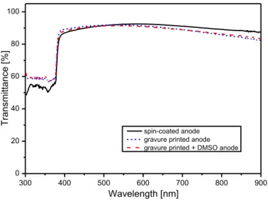
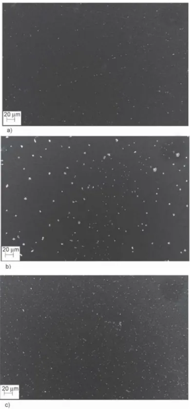
Here is reported about the realization of an high conductive (HC) PEDOT:PSS layer and subsequent DMSO post treatment completely by gravure printing technique for application as anode in flexible OLED devices.
Highly conductive PEDOT:PSS was obtained by adding DMSO (5% v/v) to the commercial Clevios PH1000 solution, as also suggested by the supplier.23 Solution was diluted with isopropyl alcohol in order to test the effects of the ink concentration on the resulting PEDOT:PSS layer. A multilayer approach was also used as further improvement of the anode layer characteristics. By this way we obtained an increase of the conductivity of the HC PEDOT:PSS layer thanks to the decrease of the sheet resistance with increasing the number of the overlapped layers, keeping high transparency.
Multilayer deposition of inks at decreasing concentration gives the best result; in fact the increase in the solvent content of the consecutive printed layers allowed to achieve values of conductivity higher than the multilayer printed at the same ink concentration.24 The multilayer approach allows a better spreading of the material in the successive printed layers and a smoothing effect of the previous printer layers; just three layers successively printed with a decreasing concentration profile are sufficient to realize a conductive layer suitable for applications as electrode.
Polyethylene naphthalate (PEN) was selected as flexible substrate for the realization of the printed anode layer. PEN is, infact, one of the most promising substrate for flexible electronic thanks to its physical-chemical properties.