Università degli Studi di Ferrara
DOTTORATO DI RICERCA IN
"SCIENZE DELL'INGEGNERIA"
CICLO XXIV
COORDINATORE Prof. Stefano Trillo
ELECTRICAL CHARACTERIZATION,
PHYSICS, MODELING AND RELIABILITY OF
INNOVATIVE NON-VOLATILE MEMORIES
Settore Scientifico Disciplinare ING/INF-01
Dottorando Tutore
Dott. Zambelli Cristian Prof. Olivo Piero
_______________________________ _____________________________
(firma) (firma)
Abstract
Enclosed in this thesis work it can be found the results of a three years long re-search activity performed during the XXIV-th cycle of the Ph.D. school in Engi-neering Science of the Universit´a degli Studi di Ferrara. The topic of this work is concerned about the electrical characterization, physics, modeling and reliability of innovative non-volatile memories, addressing most of the proposed alternative to the floating-gate based memories which currently are facing a technology dead end. Throughout the chapters of this thesis it will be provided a detailed char-acterization of the envisioned replacements for the common NOR and NAND Flash technologies into the near future embedded and MPSoCs (Multi Process-ing System on Chip) systems. In Chapter 1 it will be introduced the non-volatile memory technology with direct reference on nowadays Flash mainstream, provid-ing indications and comments on why the system designers should be forced to change the approach to new memory concepts. In Chapter 2 it will be presented one of the most studied post-floating gate memory technology for MPSoCs: the Phase Change Memory. The results of an extensive electrical characterization per-formed on these devices led to important discoveries such as the kinematics of the erase operation and potential reliability threats in memory operations. A mod-eling framework has been developed to support the experimental results and to
2
validate them on projected scaled technology. In Chapter 3 an embedded memory for automotive environment will be shown: the SimpleEE p-channel memory. The characterization of this memory proven the technology robustness providing at the same time new insights on the erratic bits phenomenon largely studied on NOR and NAND counterparts. Chapter 4 will show the research studies performed on a memory device based on the Nano-MEMS concept. This particular mem-ory generation proves to be integrated in very harsh environment such as military applications, geothermal and space avionics. A detailed study on the physical principles underlying this memory will be presented. In Chapter 5 a successor of the standard NAND Flash will be analyzed: the Charge Trapping NAND. This kind of memory shares the same principles of the traditional floating gate technol-ogy except for the storage medium which now has been substituted by a discrete nature storage (i.e. silicon nitride traps). The conclusions and the results sum-mary for each memory technology will be provided in Chapter 6. Finally, on Appendix A it will be shown the results of a recently started research activity on the high level reliability memory management exploiting the results of the studies for Phase Change Memories.
Abstract (Italiano)
Racchiusi in questo lavoro di tesi si possono trovare i risultati della trien-nale attivit´a di ricerca eseguita durante il XXIV-esimo ciclo del Dottorato di Ricerca in Scienze dell’Ingegneria svolto presso l’Universit´a degli Studi di Fer-rara. L’argomento di questa trattazione riguarda la caratterizzazione elettrica, la fisica, la modellistica e l’affidabilit´a di memorie non-volatili innovative, indiriz-zando l’argomentazione verso le tecnologie proposte a rimpiazzare nel prossimo futuro le tradizionali memorie a gate flottante, ormai proiettate verso un naturale declino tecnologico. Attraverso i capitoli di questa tesi verr´a fornita una caratteriz-zazione dettagliata dei possibili rimpiazzi delle NOR e NAND Flash nei prossimi sistemi embedded o a multi-processore. Nel Capitolo 1 verr´a introdotta la tec-nologia di memorie non-volatili con un chiaro riferimento alla tectec-nologia Flash, fornendo indicazioni e suggerimenti ad un ipotetico system designer verso il pas-saggio alla nuova generazione di memorie. Nel Capitolo 2 verr´a presentata una delle memorie della post-floating gate generation pi´u studiate nell’ultimo decen-nio: le memorie a cambiamento di fase (PCM). I risultati di una esaustiva carat-terizzazione elettrica su questa tecnologia hanno permesso di scoprire fenomeni molto importanti quali la cinetica dell’operazione di cancellazione e altre poten-ziali minacce all’affidabilit´a delle operazioni di scrittura sulle stesse. Un’intesa
at-4
tivit´a di modeling ha poi permesso di validare i risultati sperimentali in proiezione verso una tecnologia scalata. Nel Capitolo 3 verr´a mostrata una memoria per ambiente automotive: la SimpleEE p-channel. La caratterizzazione elettrica di questa memoria ha permesso di provarne la robustezza e allo stesso tempo ha aiu-tato a capire meglio il fenomeno dei bit erratici gi´a presente nelle passate NOR e NAND. Il Capitolo 4 mostrer´a gli studi eseguiti su una memoria basata su mi-cro sistemi meccanici (Nano-MEMS) provandone la capacit´a di integrazione in ambienti estremamente ostili per l’affidabilit´a come sistemi militari, geotermici e avionica spaziale. Uno studio dettagliato sui principi fisici alla base di questa memoria verr´a proposto. Il Capitolo 5 mostrer´a il successore naturale della tec-nologia Flash: le NAND Flash a intrappolamento di carica. Questo tipo di memo-rie usa gli stessi principi fisici delle memomemo-rie a floating gate per la memorizzazione dell’informazione, cambiando per´o la natura del mezzo in cui i dati vengono im-magazzinati (i.e. trappole di nitruro di silicio). Le conclusioni e il riassunto dei risultati sulle ricerche eseguite sulle varie tipologie di memoria verranno presen-tati nel Capitolo 6. In conclusione, nell’Appendice A verranno mostrati i risulpresen-tati di un’attivit´a di ricerca recentemente iniziata sulla gestione dell’affidabilit´a delle memorie ad alto livello, sfruttando i risultati degli studi delle memorie a cambia-mento di fase.
Contents
1 Introduction 1
1.1 Intrinsic Flash reliability limits . . . 2
1.2 Emerging issues of Flash technology . . . 10
2 Phase Change Memories 17 2.1 Physics of chalcogenide-based memories . . . 18
2.2 Electrical characterization of PCM arrays . . . 19
2.3 Optimization of the writing operations . . . 22
2.4 Modeling the SET kinetics . . . 33
2.5 The SET seasoning and the secondary shunt phenomena . . . 45
3 P-channel SimpleEE Memories 67 3.1 Read performance . . . 69
3.2 Program/Erase speed . . . 71
3.3 Endurance and data retention . . . 73
3.4 Disturbs robustness . . . 76
3.5 Evidence of the erratic bits . . . 79
CONTENTS ii
4.1 Device physics . . . 91
4.2 Memory architecture . . . 95
4.3 Endurance characterization . . . 97
4.4 Data retention characterization . . . 101
4.5 Environmental and mechanical characterization . . . 103
5 Charge Trapping NAND Flash Memories 106 5.1 Electrical characterization . . . 107
5.2 Program operation characterization . . . 111
5.3 Room temperature retention . . . 114
5.4 Disturbs characterization . . . 116
5.5 Edge Wordline Disturb (EWD) phenomenon . . . 121
6 Conclusions 138 A System-level reliability of non-volatile memories 140 A.1 General idea . . . 140
A.2 The physical view on PCM . . . 142
A.3 A case study . . . 143
List of Figures
1.1 FLOTOX device and its equivalent capacitance model. . . 3
1.2 Band diagram sketch of tunneling effect. . . 4
1.3 Band diagram during a program operation: without traps (solid
lines in the oxide region) and with traps (dashed lines in the oxide regions). . . 7
1.4 Threshold voltage degradation during cycling of NAND Flash
with different geometrical features. . . 7
1.5 Band diagram of the cell when programmed and not biased. The
main mechanism for data loss is tunneling through the tunnel oxide. 9
1.6 Cumulative distribution of a NAND array on Program state. Both
detrapping and SILC effects are appreciable on the time evolution. 10
1.7 Two traps assisted tunneling (2TAT) band diagram (left) and
com-parison between the SILC-2TAT model result versus the classical
LIST OF FIGURES iv
1.8 Condition for the depletion region near the gate-drain overlap re-gion of a nMOS transistor when the surface is accumulated with a low negative gate bias (a), and n+ region is depleted or inverted with high negative gate bias (b). . . 13
1.9 Leakage current measured in a nMOS transistor for different
Drain-Source voltages VDS in the subthreshold regime. When VGS approaches 0 V, for high VDS values the leakage current is due to GIDL. . . 13 1.10 Bias conditions possibly activating GIDL effects on SSL
transis-tors belonging to columns BLi−1and BLi+1. . . 14 1.11 Measured program disturbs characteristics for 3 cells belonging
to WL0, WL15 and WL31, respectively. NOP indicates the num-ber of partial programming when multiple writing of a world line is allowed for specific applications. It can be observed that, for higher values of Vpass, the disturb on cell WL0 becomes signifi-cant. . . 14 1.12 Electrostatic effect on the injection process: the Floating Gate
(FG) potential changes when an electron is injected from the sub-strate (a) to the FG (b), reducing the tunnel oxide field and the tunneling current. . . 16 1.13 Probability distributions of the injection statistics with and
with-out the contribution of the RTN (Random Telegraph Noise). . . . 16
2.1 Cross section of a PCM cell (left) and its relative graphic repre-sentation (right). . . 19
LIST OF FIGURES v
2.2 Typical PCM array topology with pnp bipolar transistors as a
se-lecting element. . . 20
2.3 Waveforms applied to each cell in the array to perform the
dy-namicI − V characterization and the extraction of Rset andVth. . 22
2.4 Result of the dynamicI − V characterization. The two curves on
display are the average over the whole cell population. . . 23
2.5 R − I characterization. The curve on display represents the
aver-age over the whole cell population. . . 24 2.6 Distribution ofVT 1,VT 2,Vs, parameters in a Gaussian probability
plot. . . 24
2.7 Average value ofVs versus the wordline index. Each point is the
average over the columns belonging to the considered wordline. . 25
2.8 Average values ofVth,VT 1,VT 2andVsduring cycling. . . 25
2.9 Average values ofImax, andRsetduring cycling. . . 26
2.10 a): MCW and BCW waveforms; b): SCOW and COW waveforms. 31
2.11 Logical flow used for waveforms optimization process. . . 31
2.12 Icell distribution dependency onVp applied within a MCW. . . 32
2.13 a): Variation ofµ criterion on MCW, in relation to Vpb): Variation ofσ criterion on MCW, in relation to Vp. . . 32 2.14 Icelldistribution dependency by appliedVp within SCOW. Similar
distribution are obtained using COW. . . 33 2.15 a): Variation ofµ criterion on SCOW, in relation to S (log-scaled)
b): Variation ofσ criterion on SCOW, in relation to S (log-scaled). 33 2.16 a): Variation ofµ criterion on COW, in relation to tH b): Variation
LIST OF FIGURES vi
2.17 Sequence of pulses used for the experiments. The SET pulse con-ditions have been: ∆t=(10ns), 25ns, 50ns and 100ns; VSET=3.5V,
3.75V, 3.9V. A total number of SET pulsesN has been applied. . . 35
2.18 Average read current for each operating condition. . . 36
2.19 Picture of the stages of the crystalline shunt formation and devel-opment. . . 36 2.20 Read current distributions after the first 5 SET pulses. . . 37 2.21 SET curves for the same cell measured 10 consecutive times
(∆t=10ns). . . 37 2.22 Average saturation current as a function of the operating conditions. 39 2.23 Read current distributions for each pulse duration. . . 39
2.24 Read current distributions for each SET voltage. . . 39
2.25 Number of Slow cells as a function of their wordline (row) posi-tion within the array. . . 40 2.26 Conductive GST model (left) and equivalent read path circuit (right). 40 2.27 Conductive GST model. A cylindric crystalline shunt
approxima-tion is used for model compactness. . . 42
2.28 Model output on different SET operative conditions. . . 44
2.29 Seasoning effect as a function of cycles number, evidenced as an
increase of the average (on 512 Kbits cells) RRESET and a
de-crease ofRSET. . . 45 2.30 Equivalent R-I characteristic of the PCM array. Characterization
LIST OF FIGURES vii
2.31 PCM cell model for measurements and connection to the array. The voltage drop on the bitline MOS selector and on BJT cell selector is accounted. . . 47 2.32 Waveform sequences for cycling with different erasing schemes
in seasoning investigation experiments. Used erasing schemes are depicted: MCW (solid), COW (dashed) and SCOW (dotted).
Waveforms parameters such asVp,tH andS are also evidenced. . 48
2.33 Average variation of the arrayRSET calculated in modulus as the
difference between two consecutive cycles measurements. . . 48
2.34 Seasoning effect evaluated on consecutive single cell measurements. 49
2.35 Average array RSET measured with a MCW erasing scheme. A
comparison with the reference read only cycling is reported. . . . 50
2.36 Average array RSET measured with a COW erasing scheme. A
dependance of the reduction of the RSET by the waveform
pa-rametertH is evidenced. . . 50
2.37 Average array RSET measured with a SCOW erasing scheme. A
dependance of the reduction of theRSET by the waveform
param-eterS is evidenced. . . 51
2.38 Average array RSET dependency from rsat within a COW
eras-ing scheme with two differenttH used. Cycle dependence is also evidenced. . . 53 2.39 PCM cell structure evidencing the seasoning phenomenon both in
LIST OF FIGURES viii
2.40 Example of RTN-like behaviors in four PCM cells observable by plotting Iread after the Erase operation versus the number of cy-cles. Two levels are evidenced (i.e. H and L in fig. d) representing
the presence/absence of the secondary path. . . 54
2.41 a) Equivalent read/write path circuit of a PCM cell. b) Program
(RESET) and Erase (SET) waveforms exploited in this work. . . . 55
2.42 Average Iread versus VSET characteristic. As shown, VSET =
3.75V holds the active material in a Partial-SET state. . . 56 2.43 Schematic description of the secondary path creation kinetics.
During the growth stage of the main percolation path, new GST crystallite grains may nucleate and subsequently join together,
contributing to the secondary path formation. . . 57
2.44 Two-states Markov chain used for modeling the secondary path presence/absence condition in PCM cells, whereη and θ represent the probability of remaining in the L and H status, respectively. . . 58 2.45 Distribution of the probabilitiesη of remaining in the L state for
three pulse durations tH of the Erase operation. The cells popu-lation prone to create the secondary shunt is identified by the first Gaussian peak withη < 0.5. . . 59 2.46 Distribution of the probabilitiesθ of remaining in the H state for
three pulse durationstH of the Erase operation. . . 60 2.47 Scatter plot of η versus θ state probabilities for tH = 2µs
(sim-ilar results are achieved for other pulse durations). The points accumulates in the center of the plot clearly evidencing a linear correlation between the two probability coefficients. . . 61
LIST OF FIGURES ix
2.48 Log-normal probability plot of the∆I distribution. . . 62
2.49 Numbers of state transitions for any set of cells characterized by the same averageL level within 200 program/erase cycles for the
three erasing times tH. Symbols denote the average number of
state transitions, whereas the error bars represent the standard de-viation from the mean value. . . 63 2.50 ∆I shifts for any set of cells characterized by the same average L
level within 200 program/erase cycles for the three erasing times
tH. Symbols denote the average ∆I shift, where the error bars
represent the standard deviation from the mean value. . . 64
2.51 Measured (symbols) and calculated (lines)Iread tail distributions after 200 Program/Erase cycles for the three pulse durations. tH = 1µs: circles and dotted line; tH = 2µs: squares and dashed line; tH = 4µs: diamond and dashed/dotted line. The full line represents
the Gaussian Model behavior fortH = 2µs. Similar Gaussian
be-havior are found for othertH values. The inset shows experimen-tal data and fitting of the main part of the distribution fortH = 2µs (the two othertH cases are almost superimposed). . . 66
3.1 Read characterization of SimpleEE modules lots. . . 70
3.2 Read benchmark between Q3 and Q4 device families. . . 71
3.3 Extracted SimpleEE array output gain at different temperatures. . 71
3.4 Program characteristics of the memory with respect to working
LIST OF FIGURES x
3.5 Erase characteristics of the memory with respect to working
tem-perature (left) and voltage exploited (right). . . 72
3.6 Endurance characteristics of the memory modules at
tempera-tures: -40◦C, 25◦C (room), 150◦C and 170◦C. . . . 73
3.7 Data retention characteristics of the memory modules at bake
tem-peratures: 100◦C, 150◦C (room), 200◦C and 250◦C. . . . 75
3.8 Average disturb on the erased (left) and programmed (right) state
for each signal configuration sorted in ascending order for a virgin device. . . 77
3.9 Average disturb on the erased (left) and programmed (right) state
for each signal configuration sorted in ascending order for a
cy-cled device (500K cycles at room temperature). . . 77
3.10 Average disturb on the erased (left) and programmed (right) state for each signal configuration sorted in ascending order for a
cy-cled device (500K cycles at room temperature). . . 77
3.11 Distributions before and after disturb application for a sample cy-cled at hot temperature (150◦C) for 500K cycles. . . . 78 3.12 p-EEPROM cell architecture (left) and table summarizing normal
operating conditions (right). . . 80 3.13 Erased (left) and programmed (right) distribution of the Flash
sample. . . 80 3.14 Erased (left) and programmed (right) distribution of the
p-EEPROM sample. . . 81
3.15 Example of erratic cell in the Flash sample. . . 81
LIST OF FIGURES xi
3.17 Examples of erratic bits in p-EEPROM device after
weak-program operation during cycling. . . 83
3.18 Examples of erratic bits in p-EEPROM device after weak-erase operation during cycling. . . 84
3.19 VT of an arbitrary p-EEPROM cell monitored during cycling
us-ing standard program waveforms. The same behavior can be ob-served on different cells and for more cycles. . . 85
3.20 Shift distribution of the erratic bits in p-EEPROM device. . . 85
3.21 Different values of energies are involved in the AHHI (Anode Hot Hole Injection) behavior of p-EEPROM and FLASH. In particu-lar, AHHI on FLASH is fed by higher energies with respect to
p-EEPROM, thus inducing more erratic behaviors. . . 86
3.22 Impact of the charge cluster on electron tunneling barrier. . . 86
4.1 Simple cantilever element for physical principles evaluation. . . . 91
4.2 The teeter-totter concept used as a MEMS switch in the arrays
characterized in this work (top) and a TEM picture of its inte-gration (bottom). The geometrical dimension of the structure are evidenced. . . 95
4.3 Read window of a Nanomech eNVM array. In this sample a read
window of more than four orders of magnitude is shown. . . 97
4.4 Benchmark of the < RCN T > between the room temperature
LIST OF FIGURES xii
4.5 Insight of the< RCN T > characteristic under room temperature endurance stress (triangles) and under the HTOL endurance stress (squares). . . 99
4.6 < RCN T > monitoring during cumulative endurance experiment. 100
4.7 < RCN T > measured for different architectures of Nanomech
eNVM. The values were calculated before and after the liquid-liquid experiment. . . 102
4.8 Reliability tests executed on NanoMEMS memories. No failing
bits. . . 104 4.9 Relative resistance drift, average across full array, for all
relia-bility tests performed on 6 alternative MEMS switch architecture variations. . . 105 4.10 Contact resistance behavior on LiquidLiquid test with 55C
-150C temperature range. The distribution shows an improvement of theRCN T after the test. . . 105
5.1 Signals applied to the array for the program operation. . . 109
5.2 Signals applied to the array for the erase operation. . . 110
5.3 Program and erase distributions measured usingIref=200nA. . . . 110
5.4 Program and erase distributions measured usingIref=400nA. . . . 111
5.5 I-V characteristics on the programmed state of an arbitrary array
string. . . 112 5.6 I-V characteristics on the erased state for same string. . . 113
LIST OF FIGURES xiii
5.8 Bitline even/odd behavior evidenced on wordline average
thresh-old voltage. . . 115
5.9 Staircase programming waveform. . . 116
5.10 Single block average program characteristic. Even/Odd bitlines separate contributions have been evidenced. . . 117 5.11 Evolution of the threshold voltage distributions of an entire array
block during a programming ramp. . . 118 5.12 Evolution of the threshold voltage distributions of cells belonging
to even bitlines only during a programming ramp. . . 119 5.13 Evolution of the threshold voltage distributions of cells belonging
to odd bitlines only during a programming ramp. . . 119 5.14 Cells number belonging to a threshold voltage bin after
applica-tion of the post-analysis data compactaapplica-tion. . . 120 5.15 Threshold voltage distribution using the ramped waveform with 1
V steps on even bitlines. . . 120 5.16 Threshold voltage distribution using the ramped waveform with 1
V steps on odd bitlines. . . 121 5.17 Retention characteristics of the array. The average retention of
the whole array, the average retention of even bitlines only and the average retention of odd bitlines only are evidenced by black, green and red curves respectively. . . 122 5.18 Threshold voltage distribution of the full device in RTB experiments.123 5.19 Threshold voltage distribution of the array even bitlines in RTB
LIST OF FIGURES xiv
5.20 Threshold voltage distribution of the array odd bitlines in RTB experiments. . . 125 5.21 Impact of read disturb on both programmed and erased cells. . . . 125 5.22 Threshold voltage measured after 1, 2, 5, ..., 200 program pulses
applied simultaneously on WL1, WL16, and WL30. . . 126 5.23 Net effect (disturb) of a program disturb measured after 1, 2, 5, ...,
200 disturb pulses applied on WL1. . . 126
5.24 Evolution of disturb on WL0 and WL2 with the number of pro-gram disturb pulses applied to WL1. . . 127 5.25 Block to block interference evaluated by monitoring both
pro-grammed and erased cells while applying program disturb pulses on WL33 of an adjacent block. . . 128 5.26 Standard NAND array architecture. The figure represents a single
block of the CT array considered in this analysis. . . 129 5.27 ISPP Pulse characteristics exploited in this work. The duration
per pulse is 4µs. . . 130 5.28 Bias conditions possibly activating the GIDL effect from GSL
transistors belonging to columns BLi−1and BLi+1. . . 131 5.29 Bias conditions possibly activating the GIDL effect from GSL
transistors belonging to columns BLi−1 and BLi+1 and theVpass disturb in unselected cells belonging to columns BLi. . . 131
LIST OF FIGURES xv
5.30 Band structure of the CT cells (excluding the TaN/Ti/TaN metal gate) considered in this work. For high biases electron B is free to tunnel into SiO2 and then gets trapped into Si3N4 layer. For low biases electron A is still able to get trapped, although the energy levels of the bands are shifted upwards. . . 132 5.31 EWD dependence on the exploited ISPP voltages during a
pro-gram operation. Vpass has been fixed at 8 V for the unselected
wordlines. . . 134 5.32 EWD dependence on the number of performed NOP on WL1.
Vpasshas been fixed at 8 V for the unselected wordlines. . . 135
5.33 EWD as a function of the NOP number. Vpasshas been varied in
order to evaluate the dependence of the phenomenon on the pass voltage. . . 136 5.34 EWD dependence on the number of write cycles performed on the
CT NAND array . . . 137 5.35 EWD as a function of the NOP number. A dependence on the
device aging is evidenced. Vpass has been fixed to 8 V for the
unselected wordlines. . . 137 A.1 Calculated write throughput comparison between the different
erasing schemes applied within a PCM. . . 147 A.2 Mean write throughput calculated with different writing
scenar-ios. The uniform traffic condition is compared with 50 writings on the data reliable area and 100, 150, 200, 300 writings on the high speed area. . . 147
LIST OF FIGURES xvi
A.3 Error probability comparison between single PCM data partitions
List of Tables
2.1 Comparison resume of the analyzed waveforms . . . 32
2.2 Seasoning impact resume with different waveform . . . 51
2.3 Parameters used for the statistical modeling of the gaussian part
of the Iread distributions extracted from the experimental data at cycle 1. . . 62
2.4 Parameters used for the fitting of the bimodal gaussian
distribu-tions ofη and θ state probability. . . 65 2.5 Parameters used for the calculation of the∆Iishift. . . 65
Chapter 1
Introduction
The last decade of research in non-volatile memories, both from academic and industrial perspective, arose potential threats to the so-called ”happy scaling” era, where the only way to achieve memory density, performance and enhanced relia-bility exploited a furious geometrical shrinking of the memory cells dimensions.
The mainstream for non-volatile memory technology in these years has been represented by the floating gate-based memories such as NOR and NAND Flash. These memories relies on a manufacturing process and on a physical storage so-lution which reached so far the maturity level. Indeed, both kind of Flash archi-tectures are reliably used either as a code memory (NOR Flash) for storing BIOS, applications and operating systems for mobile environments or as a data mem-ory (NAND Flash) relying on the high storage capacity offered by these memo-ries. The NAND Flash market segment gained particular momentum during these decades thanks to the blast of the portable applications such as digital cameras, smartphones, mp3 players, an so on. Unfortunately, these largely used compo-nents in embedded systems and MPSoCs (Multi Processing System on Chip) are
1.1 Intrinsic Flash reliability limits 2
facing difficulties in keeping up the performances and the reliability requested by a non-volatile memory components.
That explain the gained interest in these years on the so-called universal mem-ories which represent the intersection between the performances of the traditional semiconductor volatile memories such as DRAM and SRAM and the reliabil-ity offered by a non-volatile technology. The 2010 global market for emerging non-volatile random access memory products was projected to have reached 115 million USD. This market will increase to 1,590 million USD by 2015 showing an average annual growth rate of 69% per year from 2010 to 2015. In this thesis sev-eral innovative memory concepts will be analyzed as potential alternative to Flash technology. To name few of them it has been studied the Phase Change memories, SimpleEE memories, NanoMEMS memories and Charge Trapping memories.
Now it will provided a quick overview on what are the intrinsic limit of the floating gate technology and what are the emerging issues that are forcing system designers to change their mind in favor of such innovative memory technologies.
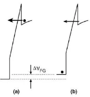
1.1
Intrinsic Flash reliability limits
The concept element of traditional Flash memory cell is a metal oxide semicon-ductor device with a floating gate electrically isolated by means of a tunnel oxide and of an interpoly oxide as sketched in Fig.1.1 [1]. The former oxide plays a basic role for the control of the device threshold voltage whose value represents, from a physical point of view, the stored information. Electrons transferred into the
float-ing gate give a threshold voltage variation∆V T = −Q
Cpp. In quiescent conditions, thanks to the two oxides, the charge stored should not leak away, thus granting
1.1 Intrinsic Flash reliability limits 3
the nonvolatile paradigm fulfillment. Oxides are available in different material depending on the Front End of Line (FEOL) process. The common materials are: pure silicon dioxide (SiO2) for tunnel oxides and a stack of Oxide-Nitride-Oxide (SiO2-Si3N4-SiO2) for interpoly oxides.
Figure 1.1: FLOTOX device and its equivalent capacitance model.
The cells are rearranged into an array organization [2] in which we can define three basic subdimensions: string, page and block. The physical mechanism used for both injecting and extracting electrons to/from the floating gate is the Fowler-Nordheim (FN) tunneling [3]. High electrical field applied to the tunnel oxide (FOX is almost 10 MV/cm) allows for electron transfer across the thin insulator to the floating gate. In NAND architectures the electronic tunneling involves the MOS channel/substrate and requires appropriate biasing of control gate and bulk terminals (see Fig.1.2), while drain and source are left floating. With respect to the Channel Hot Electron mechanism exploited for cell programming in NOR ar-chitectures, FN tunneling requires higher voltages, therefore much more complex charge pumps and higher programming times. In addition, the use of the same
1.1 Intrinsic Flash reliability limits 4
mechanism for both programming and erasing the cells exposes the tunnel oxide to a larger degradation, with possible reliability effects. These drawbacks, how-ever, are compensated by the much lower current (orders of magnitudes) required by the writing operations significantly improving power consumption and/or pro-gramming parallelism.
Figure 1.2: Band diagram sketch of tunneling effect.
During its lifetime a Flash module undergoes a large number of Pro-gram/Erase cycles. Every cycle involves very high electrical fields applied to the tunnel oxide. The reliability of the entire memory requires that the tunnel oxide is able to operate correctly under stress conditions. It is obvious that huge efforts are to be spent to determine the right process for the tunnel oxide creation (in terms of thickness, material, growth, defectivity, interface, ) in order to achieve a suc-cessful and reliable Flash technology. However, the scaling of the geometries is not helping these efforts, most of the time forcing to consider new radical design
1.1 Intrinsic Flash reliability limits 5
approaches.
The main reliability issues for Flash technology are represented by the en-durance and the data retention features.
The endurance of a memory module is defined as the minimum number of Program/Erase cycles that the module can withstand before leading to a failure. The erased and programmed distributions must be suitably separated, in order to correctly read the logical state of a cell. The difference between EV (Erase ref-erence Value) and PV (Program refref-erence Value) is defined as the ”read margin window”. However, keeping a correct read margin is not sufficient to guarantee a correct read operation: if during its lifetime the threshold voltage of an erased cell exceeds the EV limit and approaches 0 V, the current flowing through the cell may be not high enough to be identified as ”erased” by the reading circuitry, thus producing a read error. Similarly, a programmed cell could be read as ”erased” if its threshold voltage becomes lower than PV and approaches 0 V. As for the programmed distribution, it is also important that the upper threshold limit does not increase significantly with time, since a too high threshold can block the cur-rent flowing through the strings during reading operations. FN tunneling leads intrinsically to oxide degradation [4]. As a result of consecutive electron tunnel-ing, traps are generated into the oxide [5]. When filled by electrons, charged traps can increase the potential barrier thus reducing the tunneling current, as shown in Fig.1.3. Since the programming and erasing pulses feature constant amplitude and duration, less charge is transferred to and from the floating gate causing an efficiency reduction of both the program and erase operations. A narrowing of the read margin window is then expected. The charge trapped inside the oxide also produces a threshold shift∆V T directly proportional to its amount. The VT
1.1 Intrinsic Flash reliability limits 6
shift is symmetrical and increases the threshold voltage of both erased and pro-grammed cells (see Fig. 1.4). Writing waveform optimization can help in limiting the trapped charge. For example, it has been shown that the window closure can be reduced by using low voltage erasing pulses able to remove the charge accu-mulated in the oxide. As shown in Fig.1.4, the threshold voltage shifts increase with the number of program/erase operations until an endurance failure occurs. Threshold voltage shifts could be recovered by applying specific procedures, that however result not convenient when comparing their effects with the required ar-chitectural overheads and time consumption. As evidenced in Fig.1.4, the most critical effect is the increase towards 0 V of the erased threshold. To check whether all cells of a sector have been correctly erased (all threshold voltage must be below 0 V), an erase verify procedure is applied after any erase operation. It consists in a particular read operation performed by driving simultaneously all the word lines of the sector at 0V: if the read current in a bitline is 0, it means that at least a cell blocked the current flow because its threshold voltage was higher than 0 V. The entire block is marked as bad block by the memory controller and no longer addressed [2].
The retention concept instead, is the ability of a memory to keep a stored infor-mation over time with no biases applied. Electron after electron, charge loss could slowly leading up to a read failure: a programmed cell can be read as erased if its VT shifts below 0 V. The intrinsic retention is mainly limited by tunneling (see Fig.1.5) through the oxide even if thermionic emission mechanisms over the bar-rier can be considered. Recent studies [6] demonstrated that an oxide thickness of 4.5 nm is enough for granting theoretical intrinsic retention of 10 years, which is the minimum limit imposed by present standards. The cell retention worsen with
1.1 Intrinsic Flash reliability limits 7
Figure 1.3: Band diagram during a program operation: without traps (solid lines in the oxide region) and with traps (dashed lines in the oxide regions).
Figure 1.4: Threshold voltage degradation during cycling of NAND Flash with different geometrical features.
memory cycling and this effect is appreciable as a reduction of the VT levels as sketched in Fig.1.6 showing the time evolution of the cumulative VT distribution of programmed cells. Charge loss from the floating gate moves the VT
distribu-1.1 Intrinsic Flash reliability limits 8
tion towards lower values. In additions, a tail in the lower part of the distribution indicates that a small percentage of cells is losing charge faster than average. The rigid shift of the cumulative VT distribution can be related to the oxide degrada-tion within the oxide and at the Si - SiO2interface. As described early, successive electron tunneling leads intrinsically to oxide degradation, characterized by traps generation. These traps may be responsible for charge loss from the floating gate towards the silicon substrate. In fact, an empty trap suitably positioned within the oxide can activate trap assisted tunneling (TAT) mechanisms characterized by a significantly higher tunnel probability with respect to a triangular barrier unmodi-fied by the trap presence. In addition, an electron trapped within the oxide during writing operations and responsible for the VT increase leading up to endurance failures may be detrapped when the program pulse is switched off, when the cell is read or even when the cell is not addressed. As a result, the empty trap may en-hance the TAT phenomenon (assuming a positive charged trap) and, in addition, it can increase the electron field at the Floating gate-tunneling oxide interface thus raising the electron tunnel probability. The required activation energy for detrap-ping has been calculated in several experiments about 1.1 eV [7]. It is clear that these mechanisms are strongly related to the oxide degradation and therefore data retention decreases with the number of applied writing pulses. Results of reten-tion stresses showed that the cells contributing to the tails of the VT distribureten-tion are characterized by a leakage current larger than the average at the same stress level [8]. The Stress Induced Leakage Current (SILC) of these cells is attributed to TAT process of carriers through the tunnel oxide traps. By modeling the be-havior of the tail cells it has been shown that a single TAT model is not consistent with the observed leakage current. The charge loss of these cells is attributed to a
1.1 Intrinsic Flash reliability limits 9
tunneling process assisted by two traps (2TAT) - see Fig. 1.7. The characteristics of this phenomenon are the opposite with respect to detrapping: low activation energy (0.1 - 0.3 eV) and strong field acceleration. SILC affects a larger number of cells after each writing cycle, thus confirming that also this abnormal charge loss is driven by oxide degradation. The position of leaky cells within the array, however, does not show any clusterization which could be related to a techno-logical process. In addition, the abnormal leakage is not permanent: a cell can exhibit a SILC effect after a cycle and behave as normal when erased and repro-grammed. This result is consistent with a model requiring 2 traps with suitable locations within the oxide to activate a SILC effect. Some of these cells can suffer an erratic behavior [9] due to a trap annihilation/reactivation process. It has been proved, however, that traps are annealed over 85C so high temperatures partially mitigate this effect [10].
Figure 1.5: Band diagram of the cell when programmed and not biased. The main mechanism for data loss is tunneling through the tunnel oxide.
1.2 Emerging issues of Flash technology 10
Figure 1.6: Cumulative distribution of a NAND array on Program state. Both detrapping and SILC effects are appreciable on the time evolution.
Figure 1.7: Two traps assisted tunneling (2TAT) band diagram (left) and compar-ison between the SILC-2TAT model result versus the classical Fowler-Nordheim theory (right).
1.2
Emerging issues of Flash technology
As the technology scaling of Flash proceeds, emerging reliability threats have to be considered in addition to the traditional issues presented in the previous sec-tions. The influence of phenomena like the Gate-Induced Drain Leakage and the injection statistics cannot be neglected during the validation phase of a technol-ogy since they introduce new disturb types during the common operations of a module.
The Gate Induced Drain Leakage (GIDL) is a major leakage mechanism oc-curring in OFF MOS transistors when high voltages are applied to the Drain and it is attributed to tunneling taking place in the deep-depleted or even inverted region underneath the gate oxide [11]. When the gate is biased to form an accumulation
1.2 Emerging issues of Flash technology 11
layer at the Silicon surface, the surface behave like a p region more heavily doped than the substrate. This effect causes the depletion layer of the junction at the surface to be more narrow than elsewhere. The narrowing of the depletion layer near the surface increases the local electric field thus enhancing high field effects near that region. When the gate voltage in a nMOS transistor is 0 V (or below) and the Drain is biased at a high voltage, the n+ drain region under the gate can be depleted or even inverted (see Fig.1.8). This effect causes a peak field increase leading up to high field phenomena such as avalanche multiplication and band-to-band tunneling. The band-to-band-to-band-to-band tunneling probability can also be increased by the presence of surface traps, resulting in a band-trap-band tunneling. As a result of these effects, minority carrier are emitted in the drain region underneath the gate and swept laterally to the substrate which is at a lower potential, thus completing a path for the leakage current. Fig.1.9 shows the sub-threshold characteristics in an nMOS transistor for different Drain voltages [12]. On NAND arrays the GIDL has been found to produce erroneous programming in specific cells, that is those belonging to WL0, adjacent to the SSL transistor. The SSL transistor is OFF dur-ing programmdur-ing and GIDL effects may be present if its drain is driven at high voltages. This situation occurs because of the self-boosting techniques adopted to prevent programming. As shown in Fig.1.10, if WL0 is driven at Vpgm to program the cell in the central column, the channel voltage of the cells sharing the WL0 line are to be raised to prevent their programming. Because of the self-boosting technique, the source terminal of those cells (therefore also the drain node of their adjacent SSL transistors) are raised to values higher than VCC, thus leading up to bias configurations activating GIDL effects. The electron-holes pair generation follows and the generated electrons are accelerated at the SSL - WL0
1.2 Emerging issues of Flash technology 12
space region and can be injected as hot electrons in the floating gate of WL0 cells. Also the DSL transistors may trigger GIDL mechanims when boosting effects take place on cells sharing WL31, but since the voltage applied to the DSL gate line is VCC, the consequences suffered by cells belonging to WL31 are much lower with respect to those sharing WL0. Fig.1.11 shows experimental data for 3 differ-ent cells: WL0 and WL31, potdiffer-entially affected by GIDL disturbs, and a reference one located in the middle of the string. This unwanted programming in specific cells is supposed to burden in scaled architectures, since a reduced separation be-tween WL0 and SSL lines will increase the accelerating fields for hot electrons. Recently, to mitigate GIDL effects, it has been proposed to introduce two dummy world lines to separate the two select transistors and the effective string of cells. To reduce the impact of these two additional word lines, longer strings of 64 cells have been proposed to improve area efficiency. A higher number of cells in series (64 cells vs 32 of standard architectures), however, increase the string resistance so that word-line voltage modulation are required during read and programming thus ensuring that proper voltage levels are applied depending on the cell location within the string. For instance, a higher word-line voltage is used when accessing a cell near the top of the string (close to the bit line) to compensate for the string resistance.
The aggressive scaling of Flash memories, necessary to improve their perfor-mances, brings attention also to the discrete nature of the charge stored in the floating gate. The number of electrons determining the stored information, in fact, continuously decreases with the tunneling area dimension. When only few electrons control the cell state (i.e. setting the transistor threshold voltage), their statistical fluctuations determine a non-negligible spread. These fluctuations may
1.2 Emerging issues of Flash technology 13
Figure 1.8: Condition for the depletion region near the gate-drain overlap region of a nMOS transistor when the surface is accumulated with a low negative gate bias (a), and n+ region is depleted or inverted with high negative gate bias (b).
Figure 1.9: Leakage current measured in a nMOS transistor for different Drain-Source voltages VDS in the subthreshold regime. When VGS approaches 0 V, for high VDS values the leakage current is due to GIDL.
be attributed to the statistics ruling the electron injection into the floating gate during program or to the electron emission from the floating gate during erase or retention, both related to the granular nature of the current flow [13]. A slight vari-ation of the number of electrons injected during programming may produce VT
1.2 Emerging issues of Flash technology 14
Figure 1.10: Bias conditions possibly activating GIDL effects on SSL transistors belonging to columns BLi−1and BLi+1.
Figure 1.11: Measured program disturbs characteristics for 3 cells belonging to WL0, WL15 and WL31, respectively. NOP indicates the number of partial pro-gramming when multiple writing of a world line is allowed for specific applica-tions. It can be observed that, for higher values of Vpass, the disturb on cell WL0 becomes significant.
variations possibly leading to errors in MLC architectures. Cells in NAND MLC architectures are programmed by using a staircase voltage on the control gate.
1.2 Emerging issues of Flash technology 15
This kind of waveform allows achieving a constant current Fowler-Nordheim tun-neling: by increasing the wordline voltage after each short pulse it is possible to compensate the field reduction that follows the electrons injection into the float-ing gate (see Fig.1.12). For sufficiently large step numbers, a linear VT increase
is obtained, with a ∆V T per step almost equal to the applied voltage step but
leading to a significant VT distribution enlargement (see Fig.1.13). This is due to the programming current convergence toward an equilibrium stationary value, corresponding to an average number of electrons transferred to and from the float-ing gate for each step [14]. The discrete nature of the charge flow introduces, for each cell, a statistical spread contribution to the resulting VT after each step. It has been evidenced that the threshold voltage variation spread, indicated asσ∆V T, depends only on the parameter Vstep of the programming waveform (i.e. on the
injected charge per step qn) and not on the pulse duration and on the number of
1.2 Emerging issues of Flash technology 16
Figure 1.12: Electrostatic effect on the injection process: the Floating Gate (FG) potential changes when an electron is injected from the substrate (a) to the FG (b), reducing the tunnel oxide field and the tunneling current.
Figure 1.13: Probability distributions of the injection statistics with and without the contribution of the RTN (Random Telegraph Noise).
Chapter 2
Phase Change Memories
Phase Change Memory (PCM) is one of the most promising emerging Non-Volatile Memory (NVM) technology thanks to fast writing operations, long en-durance and very good radiation hardness. PCMs offer direct write (any bit can be independently reprogrammed with no need for block erasing), improved write throughput versus NOR-based memories and random access time versus NAND-based memories, as well as the potential to be scalable beyond Flash technol-ogy [15]. Moreover, PCMs ensure high endurance and good compatibility with standard CMOS fabrication processes. Although a relevant effort is still being put on design optimization and material analysis, the PCM technology has today reached a significant level of maturity so that test chips containing multimegabit arrays of cells are commonly available for electrical characterization purposes. As a result, a significant amount of statistical information can be provided to the reliability/cell design engineer.
2.1 Physics of chalcogenide-based memories 18
2.1
Physics of chalcogenide-based memories
In PCMs, the storage device is made of a thin film of chalcogenide alloy (in our case, Ge2Sb2Te5, GST) [16]. This material can reversibly change between an amorphous (high impedance, RESET state) and a polycrystalline (low impedance, SET state) phase when thermally stimulated via Joule heating, thus allowing infor-mation storage. The phase conversion of a storage element is obtained by appro-priately heating (by means of electrical pulses applied to a suitable heater element) and then cooling a small, thermally isolated portion of the chalcogenide material. Fig. 2.1 shows a cross section of a PCM cell and its relative graphic representation. Once the chalcogenide material melts, it completely loses its crystalline structure. When rapidly cooled, the chalcogenide material is locked into its amorphous state (to this end, the cooling operation rate has to be faster than the crystal growth rate). To switch the memory element back to its crystalline state, the chalcogenide ma-terial is heated to a temperature between its glass transition temperature and its melting point temperature [17]. In this way, nucleation and micro-crystal growth occur in tens of nanoseconds, thus leading to a (poly)crystalline state. From above, it is apparent that the storage element can be modeled as a programmable resistor (high resistance = logic 0; low resistance = logic 1). Reading a cell basically con-sists in measuring the resistance of the addressed storage device. To this purpose, a predetermined voltage is forced across the storage element of the selected cell, and the resulting current flow is sensed.
2.2 Electrical characterization of PCM arrays 19
Figure 2.1: Cross section of a PCM cell (left) and its relative graphic representa-tion (right).
2.2
Electrical characterization of PCM arrays
All characterization measurements have been performed on a 512 Kbit popula-tion of PCM cells with the aid of a dedicated testing equipment. Fig. 2.2 depicts
a detail of the memory cell integrated in an array environment. A pnp Bipolar
Junction Transistor (BJT) is employed as the cell selector in order to minimize silicon area occupation, and, hence, improve data storage density. Read voltages and write voltages are transferred to the cells through a select nMOS transistor supplied by Vpp = 4.8V . A heater resistance Rh is in series with RGST, repre-senting the resistance of the GST active element. Details on the 180 nm PCM technology characterized in this thesis can be found in [18]. The read current of the cell can be measured in a Direct Memory Access mode by applying a read voltage at the control gate of the select nMOS transistor. The SET and RESET operations are performed similarly by applying a SET/RESET pulse at the control
2.2 Electrical characterization of PCM arrays 20
Figure 2.2: Typical PCM array topology withpnp bipolar transistors as a selecting element.
gate of the select nMOS transistor.
A set of Relevant Electrical Parameters (REP) has been defined and character-ized on test chip arrays [19]: Vth,VT 1,VT 2,Vs,Imax, andRset. REP are intended to provide a synthesis of results obtained from key characterization procedures which are commonly adopted on single cell study. The synthesis becomes impor-tant when the same procedures are applied to a population of cells. The dynamic I − V characteristics describe both the SET curve and the RESET curve which
2.2 Electrical characterization of PCM arrays 21
are measured by applying the sequence of pulses shown in Fig. 2.3a-b. Fig. 2.4
shows theI − V curves obtained by averaging the I − V curves of all the cells
of the array. These curves can be described in terms of at least two parameters which can be easily extracted from the data: Rset andVth. When a complete IV characterization is performed for each cell of a 5I2K population, 80MB of data are collected, whereas the extraction of REP allows a more easy analysis on 4MB of synthetic data only. TheR − I curve describes the read current (or equivalently the resistance) as a function of the SET pulse amplitude. TheR − I curve is mea-sured by applying the sequence of pulses shown in Fig. 2.3c. Fig. 2.5 shows the R − I curve obtained by averaging the R − I curves of all the cells of the array. These curves can be described in terms of four parameters which can be easily extracted from the data:VT 1,VT 2,Vs,Imax.
When a completeR − I characterization is performed for each cell of a 512
Kb population, 60MB of data are collected, whereas the extraction of REP allows a more easy analysis on 8MB of synthetic data only. The usage of synthetic pa-rameters allows the analysis of statistical behavior of a cell population as shown in Fig. 2.6. From these graphs it is possible to evidence some anomalous behavior like, for example, the one shown in theVs distribution which exhibits a tail at its lower left corner. A further analysis ofVs over the whole cell population allows to show that this feature is related to the array architecture and in particular to the cell distance from the bitline strap contact (see Fig. 2.7). Standard reliabil-ity cycling tests can be performed and results effectively displayed by using REP. Fig. 2.8 shows the behavior of the cell population displaying the average values of Vth, VT 1, VT 2 andVs during a 1M SET/RESET cycle experiment. This figure summarizes significant results. The switching threshold value decreases during
2.3 Optimization of the writing operations 22
Figure 2.3: Waveforms applied to each cell in the array to perform the dynamic I − V characterization and the extraction of RsetandVth.
cycling although only after some hundred thousands cycles. This phenomenon has to be taken into account in the design of the reading voltage. There is also an increase ofVT 2which can interfere with the RESET operation. Fig. 2.9 shows the
increase of the maximum current of theR − I curve and the decrease of the SET
resistance with cycling. This result clearly indicates that cells undergo a better crystallization with cycles, a phenomenon sometimes called cell seasoning.
2.3
Optimization of the writing operations
Different voltage waveforms are used for both programming (or RESET) and eras-ing (or SET) operations in PCM, referreras-ing to the GST amorphization and crystal-lization processes, respectively. The main differences consist on the voltage, the
2.3 Optimization of the writing operations 23
Figure 2.4: Result of the dynamic I − V characterization. The two curves on
display are the average over the whole cell population.
length, and the shape of the applied waveforms. Typically, the programming op-eration is achieved by using a voltage pulse, bringing the GST above its character-istic melting point, then cutting away the pulse rapidly, in order to melt and then amorphize the GST. The erasing operation, instead, can be achieved in many ways, due to multiple possibilities for achieving crystallization of active chalcogenide. Many reliability issues of multimegabit memory arrays have been tackled in the last few years, mainly concerning the used phase change materials and the cell geometrical parameters. However, a detailed analysis of the impact of waveform parameters on the overall reliability of large arrays is still missing, in particular for the erasing case where the randomness of the crystal nucleation physics in chalcogenide materials plays a basic role [17].
2.3 Optimization of the writing operations 24
Figure 2.5: R − I characterization. The curve on display represents the average
over the whole cell population.
2.3 Optimization of the writing operations 25
Figure 2.7: Average value of Vs versus the wordline index. Each point is the
average over the columns belonging to the considered wordline.
2.3 Optimization of the writing operations 26
Figure 2.9: Average values ofImax, andRset during cycling.
crystal grains inside the programmable region (PR) and then ensure a low resis-tivity path between the cell polycrystalline GST and the heater. Crystal grain creation follows a nucleation dynamic [17], taking place pseudo-randomly inside the whole active area, following the electrical field distribution generated by the voltage waveform.
To compare and optimize erasing waveforms some comparison criteria are to be introduced:
• Number of waveform parameters. Each waveform has a typical set of pa-rameters that can be varied in order to achieve the desired erasing target. Having more parameters, a greater complexity is introduced during the waveform analysis.
• Array current mean value µ [µA]. This parameter is a target for erase oper-ation. It mainly represents the endpoint of the crystallization process.
2.3 Optimization of the writing operations 27
• Array current standard deviation σ [µA]. The distribution of the cells read currents after erase,Icell, is found to follow a gaussian behavior. The stan-dard deviationσ is an indicator of how the erasing algorithm is able to keep the distribution compact.
There are three common approaches for achieving erasing operation:
• Melt and crystallize: the formation of the low resistive path is preceded by a melting operation in the PR.
• Crystallize once: the phase transition from amorphous to crystal is achieved by applying to the cell a voltage below the melting pointVm
• Burst crystallization: the grain nucleation is achieved by a sequence of short voltage pulses applied to PR.
Each method requires suitable waveforms. Optimization is achieved by following the flow represented in Fig.2.11.
Melt and Crystallize Waveform (MCW) belongs to the melt and crystallize approach. It is constituted by two parts: the former is a linear drop from a peak voltageVp higher thanVm to 2 Volts; the latter is a rapid (≈ 10 ns) voltage cut to 0 V (see Figs.2.10a). The initial part of the waveform must provide a sufficient heat inside PR, driving it to melt. Once the GST is completely molten the suc-cessive crystallization process starts from a fully amorphized material where pre-crystallized spots within PR have been certainly removed. Crystallization starts when the waveform is aboveVmand ends slightly above 2 Volts, so that the grain formation and the percolation path creation is a slow process. MCW allows get-ting low σ values (thus compact distributions), but it is difficult to control the µ
2.3 Optimization of the writing operations 28
value. MCW is also called a one parameter waveform, since onlyVp can be
opti-mized. As can be seen in Fig.2.12, by lowering this parameter theIcelldistribution broadens significantly and a large tail for lowIcell values is observed. This is re-lated to the erasing approach followed by MCW: if Vp is not sufficiently larger thanVmthe crystallization process does not necessarily starts from a fully molten material and the subsequent dynamics can vary from cell to cell. A too large Vp, however, may overstress the GST structure due to the melting process. Since MCW may produce the tightest distribution with respect to the other waveforms, the limitation ofσ can be the optimization goal. Therefore Vp could be increased
until the required σ has been reached. Fig.2.13a and Fig.2.13b confirm the poor
ability to control the crystallization dynamic, showing the rapid saturation of µ andσ values.
Sloped Crystallize Once Waveform (SCOW) is used for a crystallize once
approach. Its shape is that of a rectangular trapezium, with Vp < Vm (see
Figs.2.10b). The crystallization process starts from the previous amorphous state. After a hold time tH, in which the voltage is kept at Vp, the voltage is linearly driven to 0, waiting for the complete crystal grains formation. The controlled pa-rameters are: Vp, that influences the crystal grains formation speed, tH, the time tsrequired to reach 0 V, which also define the slope (S) parameter as S = Vp/ts. The availability of 3 adjustable parameters makes SCOW also suitable for multi-level applications, since the average current value can be controlled while keeping a tight distribution. SinceVp is mandatory for knowledge of crystallization speed, is therefore requested a determination of its optimum value, thus granting an
ac-ceptable trade-off between compactness of Icell and higher read window margin.
2.3 Optimization of the writing operations 29
distribution, due to unwanted melting, that can occur in cells characterized by a Vmvalue lower than the expected for the array. Same tails appears whenVp is not sufficiently larger to grant correct crystallization. The best solution evaluated, that
will be furthermore used for BCW and COW, isVp = 3.75 V.tH has been found
to affect only theµ parameter, so that it can be conveniently adjusted to shift the entireIcelldistribution in multilevel application. The slopeS, on the contrary, in-fluences also theσ parameter and therefore it must be optimized in order to tighten theIcell distribution. Fig.2.15a and Fig.2.15b show theµ and σ dependency on S.
An optimized valueS = 1 is found.
Crystallize Once Waveform (COW) and Burst Crystallize Waveform (BCW) are used for a crystallize once approach and are characterized by a rectangular shape (see Figs.2.10b). With respect to SCOW the crystallization process ends abruptly. The key parameter istH, that allows controlling the average read current after erase, making COW also suitable for Multi-levels architectures. A too short
tH may otherwise provoke parasitic programming phenomena, especially if
tH ≤ td (2.1)
wheretdis the characteristic delay requested by PR to create the percolation path. It has been decided to group the COW and the BCW optimization, due the evident similarity of the waveforms. The main difference consists in the presence of theR parameter on the BCW, which allows to implement the burst crystallization pro-cess using the crystallize-once mechanism as base. The COW waveform is
char-acterized by two parameters: Vp andtH. BCW can replace COW when a deeper
2.3 Optimization of the writing operations 30
memories) is required in multi levels architectures (see Figs.2.10a). This wave-form realizes theburst crystallizationapproach and it is constituted by a sequence of short box pulses. The physical mechanism behind the crystal grains formation is a slight variation of that achieved by COW, since the pulse is removed before the complete grain formation. A burst of COWs is applied, thus creating a sort of temperature elastic effect, in which the temperature rise (well below the melt-ing point) increases the crystallization process speed, while the temperature fall induces a stabilization of the grain size. The three BCW characteristic parameters are: Vp, the pulse durationtH and the repetition numberR of the standard pulse. The first two parameters are the same of COW, so that they influence theIcell in a similar way. The last parameter is only used to reach longer exposure times. Critical issues related to the use of BCW may arise if (2.1) is not respected or if the typical RC delays of the chip circuitry are not correctly taken into account, which may force crystal grains to be reabsorbed into amorphous structure. It has
been first analyzed the dependance on Vp with the same methodology used for
SCOW, finding an optimal value of 3.75 V, resulting in the lowest σ and in the
smallestIcell distribution tail (see Fig.2.14). As fortH, a strong dependance has been found for bothµ and σ criteria, only for very short times (see Fig.2.16a and Fig.2.16b). This result can be explained by the nucleation dynamics: the finalIcell value saturates after the end of the crystal grains growth phase [19] (occuring, in this study case, after≃ 500 ns).
The performed study can be further extended to non-common erasing wave-forms such as full exponential (ECOW) and ramped exponential (RECOW). Table 2.1, resume the details of the analyzed waveforms.
2.3 Optimization of the writing operations 31
Figure 2.10: a): MCW and BCW waveforms; b): SCOW and COW waveforms.
Waveform Selection parameter ? One degree START NO Choose freedom σ read margin (ML) YES END Tune other parameters in order to get lowest
for greater µ and highest
2.3 Optimization of the writing operations 32 20 30 40 50 60 70
I
cell[µA]
0.001 0.0010.01 0.1 1 10 10 50 50 90 99 99.9 99.99 99.999Percentage [%]
Vp = 5 V Vp = 5.5 V Vp = 6 V Vp = 6.5 V VpFigure 2.12:Icelldistribution dependency onVp applied within a MCW.
5 5.5 6 6.5 Vp [V] 40 45 50 55 60 µ [ µ A] 5 5.5 6 6.5 Vp [V] 0 0.5 1 1.5 2 2.5 3 3.5 4 σ [ µ A]
Figure 2.13: a): Variation ofµ criterion on MCW, in relation to Vp b): Variation ofσ criterion on MCW, in relation to Vp.
Table 2.1: Comparison resume of the analyzed waveforms
MCW SCOW COW BCW
Parameters Number 1 3 2 3 (2)
µ controllability None Coarse Excellent Excellent
σ reduction Excellent Good Bad Bad
2.4 Modeling the SET kinetics 33 0 10 20 30 40 50 60 70
I
cell[µA]
0.001 0.0010.01 0.1 1 10 10 50 50 90 99 99.9 99.99 99.999Percentage [%]
Vp = 3.25 V Vp = 3.5 V Vp = 3.75 V Vp = 4 V VpFigure 2.14: Icell distribution dependency by applied Vp within SCOW. Similar
distribution are obtained using COW.
100 101 102 S [V/µs] 35 38 40 42 45 µ [ µ A] 100 101 102 S [V/µs] 2 4 6 8 σ [ µ A]
Figure 2.15: a): Variation of µ criterion on SCOW, in relation to S (log-scaled) b): Variation ofσ criterion on SCOW, in relation to S (log-scaled).
2.4
Modeling the SET kinetics
Electronic switching is the fundamental mechanism of Phase Change Memory governing the transition from the RESET state to the SET state [20, 21]. The physics behind this mechanism still remains a puzzle and, although various phys-ical models [20, 21] have already been proposed in literature, their validation has been carried out mostly through single cell electrical characterization. On the
2.4 Modeling the SET kinetics 34 0 0.5 1 1.5 2 2.5 3 3.5 4 t H [µs] 10 20 30 40 50 60 70 µ [ µ A] 0 0.5 1 1.5 2 2.5 3 3.5 4 t H [µs] 0 2 4 6 8 10 12 14 16 σ [ µ A]
Figure 2.16: a): Variation ofµ criterion on COW, in relation to tH b): Variation ofσ criterion on COW, in relation to tH.
other side, the statistical nature of the electronic switching process would require a relatively larger cell population to be analyzed in order to give a more complete picture of the whole phenomenon. In particular, it has been found [17] that a certain delay time (td) is necessary in order to form a polycrystalline grain perco-lation path (shunt) between the bottom electrode and the top electrode across the Ge2Sb2Te5 (GST) material. When this condition occurs, cell resistance rapidly drops to small values. It is possible to model the delay time in terms of simple analytical formulae which take into account the average behavior and the param-eter dependence on both technological paramparam-eters and operating conditions [17]. However any detailed statistical description of the shunt formation time has never been presented and, more in general, also any statistics related to the whole crys-tallization process involving nucleation, growth and saturation, has never been shown. Experimental results provide a statistical description of the delay time and are consistent with the delay time model proposed in [17], also revealing some interesting features of crystal growth dynamics and its saturation.
All experimental results have been measured and collected by using a dedi-cated testing equipment called Rifle developed by Activetechnologies. All wave-forms have been externally applied by the instrument on a 8Mb PCM test chip
2.4 Modeling the SET kinetics 35
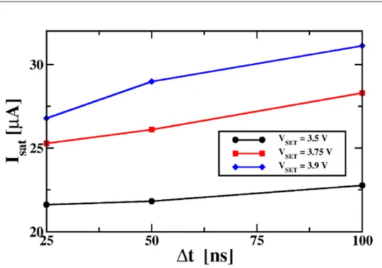
featuring 180nm technology. All data shown in this work refer to 512Kb popu-lations. Fig.2.17 shows the waveform and the sequence of operations performed during the measurement. We used sequences of short SET pulses with durations ∆t=(10ns), 25ns, 50ns and 100ns and amplitudes VSET=3.5V, 3.75V, 3.9V. The
number of pulsesN has been adjusted in order to keep constant Nx∆t=1µs for
each condition. After each pulse we measured the read current (Iread) of each
cell of the array, thus obtaining a SET curve for each cell of the population (Iread versus time).
Figure 2.17: Sequence of pulses used for the experiments. The SET pulse
condi-tions have been: ∆t=(10ns), 25ns, 50ns and 100ns; VSET=3.5V, 3.75V, 3.9V. A
total number of SET pulsesN has been applied.
During nucleation stage 2 shows the average SET curves measured in each
operating condition. A significant dependence on both ∆t and VSET is clearly
visible in Fig.2.18. Each set curve can be divided into three parts each corre-sponding to specific stages of the crystallization process (see Figure Fig.2.19):
nucleation, growth and saturation. During nucleation crystals of radius Rc


![Figure 2.34: Seasoning effect evaluated on consecutive single cell measurements. allow a further parametric analysis [25].](https://thumb-eu.123doks.com/thumbv2/123dokorg/4707098.45104/73.918.259.733.149.414/figure-seasoning-effect-evaluated-consecutive-measurements-parametric-analysis.webp)
