Università degli Studi di Salerno
Dipartimento di Ingegneria Elettronica ed Ingegneria Informatica Dottorato di Ricerca in Ingegneria dell’Informazione
XI Ciclo – Nuova Serie
T
ESI DID
OTTORATOModels and methods for the
design of isolated power
converters in high-frequency
high-efficiency applications
C
ANDIDATO:
G
IULIADI
CAPUA
T
UTOR:
P
ROF.
N
ICOLAFEMIA
C
OORDINATORE:
P
ROF.
A
NGELOMARCELLI
I dedicate this achievement
to my sister Alessia
Thank you for your support, encouragement and love.
Acknowledgements
First of all, I would like to thank Prof. Nicola Femia for his supervision, encouragement and his invaluable advice throughout my Ph.D. program. His profound knowledge and creative thinking have been source of inspiration throughout this work. I am really grateful for the opportunity to work with him, whose daily and constant presence has greatly contributed to my development, as a student and as a person. From May 18, 2009 something has changed in my life, thanks to him.
I would also like to thank all my past and present colleagues from the Lab T17’ Power Group, for their friendship, for their help, for their support, for the good times we spent together, for the reflections and the lessons of life which made me become the person I am. This is not a complete list, but I would as well to remember some of those who have accompanied me in these latest years in the Lab T17: Mario Fortunato, Raffaele Alfano, Vincenzo Carpentieri, Maria Luisa Cruoglio, Antonietta De Nardo, Andrea Cantillo, Walter Zamboni, Francesca Mazziotti, Annamaria Ceccia, Mariella Corvino, Martino Romano, Andrea Caruso, Stefania Crucito, Edoardo Cavallaro, Alex Hernandez, Gianluca Vicidomini, Vincenzo Gallifuoco, Francesco Savarese, Roberto Parisi, Antonio Contursi, Emilio Mamarelis, Massimiliano De Cristofaro, Davide Toledo, Evelina Iovino, Michela Avagliano.
Finally, a special thanks to my parents, for their encouragement and their patience, especially for all those moments in which I have no time, for understanding me and my projects, for supporting me in these 25 years of studies. I hope that you can be always proud of me, like I am of you. And thanks to my beloved sister Alessia, simply for being the most important person in my life.
Contents
CONTENTS ... 3
INTRODUCTION ... 7
CONSIDERATIONS ... 13
REFERENCES ... 17
CHAPTER 1.SWITCHING MODE POWER SUPPLIES ISOLATED CONVERTER ... 3
1.1ISOLATED CONVERTERS OVERVIEW ... 3
1.2ISOLATED CONVERTERS TOPOLOGIES ... 4
Flyback Converter ... 4
Forward Converter ... 5
Active Clamp Forward Converter ... 5
Push-Pull Converter ... 7
Half-Bridge and Full-Bridge Converter ... 7
COMMENTS ... 9
REFERENCES ... 10
CHAPTER 2.TRANSFORMER DESIGN FOR ISOLATED CONVERTERS ... 11
2.1INTRODUCTION ... 11
2.2DESIGN METHODS FOR MAGNETIC DEVICES ... 15
2.2.1 The Ap Design Method ... 15
2.2.2 The Kgfe Design Method ... 18
2.3THE KC AND KFGEOMETRIC FORM FACTORS ... 22
2.4DESIGN EXAMPLES ... 25
2.4.1 Thin cores vs Thick cores ... 31
2.4.2 Duty-Cycle and Switching Frequency investigation ... 32
2.5EXPERIMENTAL VERIFICATIONS ... 34
REFERENCES ... 41
CHAPTER 3.TEMPERATURE EFFECTS ON TRANSFORMERS DESIGN CONSTRAINTS ... 45
3.1TRANSFORMER THERMAL MODEL AND GFFS ... 45
3.2ACCEPTABILITY BOUNDARY CURVE FOR MAGNETIC CORES SELECTION ... 55
3.2.1 Case Study ... 58
COMMENTS ... 66
4 Contents
CHAPTER 4.MOSFETS COMMUTATIONS ANALYSIS ... 69
4.1STATE OF ART AND RESEARCH GOALS ... 69
4.2MOSFETSRSC COMMUTATIONS ANALYSIS ... 75
4.3MOSFETS SRSC COMMUTATIONS ANALYSIS WITH MFE METHOD ... 83
4.4NUMERICAL SIMULATION OF SRSC COMMUTATIONS ... 90
4.4.1 Case Study #1 ... 90
4.4.2 Case Study #2 ... 94
4.4.3 Case Study #3 ... 102
4.5EXPERIMENTAL TESTS ... 108
4.5.1 Experimental Activity improvements... 112
COMMENTS ... 118
REFERENCES ... 119
CHAPTER 5.SYSTEM LEVEL ANALYSIS OF AN ACTIVE CLAMP BASED FORWARD CONVERTER ... 125
5.1FORWARD ACTIVE CLAMP OVERVIEW ... 125
5.2STRESSES CONSTRAINTS IN LS-FAC ... 127
5.3ZVS INVESTIGATION IN LS-FAC ... 136
5.4EXAMPLE OF ZVS VERIFICATION ... 144
5.4.1 Simulations vs Experimental Measurements ... 153
REFERENCES ... 160
CONCLUSIONS AND FUTURE WORKS ... 165
APPENDIX A.SIMPLIFIED MODELS FOR SWITCHING LOSSES EVALUATION ... 169
REFERENCES ... 175
LIST OF SYMBOLS ... 177
Introduction
Power supply technology is an enabling technology that allows us to build and operate electronic circuits and systems [1].
Today, many electronic systems require several dc supply voltages, which are usually derived from a battery or an ac utility line using a transformer, rectifier and filter. The resultant dc voltage is not constant enough and may contain a high ac ripple that is not appropriate for most applications. Voltage regulators are used to make the dc voltage more constant and to attenuate the ac ripple. A Power Supply (PS) is a constant voltage source with a maximum current capability.
PSs are used in telecommunications, instrumentation equipments, computers, aerospace, automotive, motor control, renewable energy, medical, lighting, defense electronics; in other words, wherever efficient energy processing is needed. Designers needs to properly select the technology of each PS, according to system finality in which it is going to work [2][3]. Important issues influencing this choice are:
cost; efficiency;
weight and volume; heat dissipation; reliability;
number of required output voltages; EMI;
time-to-market.
There are two general classes of PS: regulated and unregulated. The output voltage of a regulated PS is automatically maintained within a narrow range, 1÷2% of the desired nominal value, in spite of line voltage, load current, and temperature variations. A regulated dc PS is also called dc voltage regulator.
Two major power supply technologies can be recognized in the development of regulated power supplies system: linear regulators and switching-mode power supplies [1]-[3].
In linear voltage regulators, transistors are operated in active region as dependent current sources, with relatively high voltage drops at high currents, dissipating a large amount of power and resulting in low efficiency (around 35-50%). Because their losses are dissipated as heat, linear regulators are commonly used in equipments where heat generation and low efficiency are not of major concern. However, they exhibit low noise level, resulting suitable for audio applications, data converters and wherever low cost and quick design are desired.
In switching-mode converters, transistors are operated as switches, which inherently dissipate much less power than transistors operating as dependent current sources. The voltage drop across the transistors is very low when they conduct high current and the transistors conduct a nearly zero current when the voltage drop across them is high. Therefore, the conduction losses are low and the efficiency of switching-mode converters is high, usually above 85–95%.
In switching-mode converters two main PS technologies can be found: PWM regulators and resonant regulators. Both can be used at high power and voltage levels, are small in size, light in weight, and may achieve high conversion efficiency. PWM regulators are more efficient and flexible in their use than linear regulators [4][5]. Their weight is much less that linear regulators, since they require less heatsinking for the same output ratings. However, because of switching losses increase proportionally to switching frequency, losses reduce the efficiency at high frequencies. Resonant converters are commonly used in applications where still lighter weight and smaller size are desired and, above all, a reduced amount of noise is acceptable [5].
Both PWM and resonant switching-mode converters are more expensive and require more engineering development, and are adopted as in non-isolated as in isolated conversion [5]. In a large number of applications, dc isolation between the input and output of the converter is desired: for example, in all off-line applications, where the input of the converter is directly connected to the ac utility system. In such a case, transformer is introduced into the switching converter
Introduction 9 because of isolation requirements. Moreover, when a large step-up or step-down conversion ratio is required by the application specifications, the use of a power transformer can allow to achieve better converter optimization due to the distribution of stresses among power components, compared with non isolated topologies. In fact, by proper combined choice of transformer and silicon devices, voltage and current stresses on transistors and total power losses can be minimized, improving both efficiency and cost of the switching-mode isolated converter. Isolated converters are also very effective solutions in multi-output power supplies, thanks to the use of multiple secondary windings transformers. The counterpart of benefits offered by transformers lies in the need of a careful design at system level in order to achieve a good trade-off among overall performances, size, cost and reliability.
PWM converters usually work under hard switching conditions, with semiconductor devices voltages and currents changing abruptly from high values to zero and vice-versa at turn-on and turn-off, thus causing switching losses and a great amount of electromagnetic interference noise (EMI) [4]. In PWM dc–dc converters, higher power density and faster transition response can be obtained mostly by increasing the switching frequency. Nevertheless, as the switching frequency increases, efficiency decreases and EMI increase as, when MOSFETs are used as switching device in power converters, the losses occurring due to the charge/discharge of their parasitic capacitances increase with frequency [6]. In order to reduce losses and improve PWM converters efficiency, improved semiconductor devices and magnetic materials have been developed over the last decades [7]. For example, NexFET™ technology is a new generation of silicon-based power MOSFETs with an inherently low-charge structure and very low on resistance and parasitic capacitances [8]. NexFET™ technology delivers high performance for both N and P channel power MOSFET devices, increasing efficiency in existing switching converters, as well as enabling the next generation of switching power converters operating at switching frequency of several MHz. In high voltage MOSFETs panorama, CoolMOS™ is an interesting technology of power MOSFETs, characterized by reduced gate charge, optimized gate threshold voltage for soft-switching, good body-diode
ruggedness, improved dv/dt [8]. All these features permit to achieve improved efficiency.
In isolated converters, the transformer leakage inductance forms resonant circuits with the silicon devices parasitic capacitances, causing ringing phenomena, which can lead to efficiency degradation, unless they are adequately exploited to realize some form of soft-switching. Indeed, switching losses and EMI level in PWM converters can be both reduced by soft switching techniques. Numerous soft-switching circuit techniques have been proposed and discussed in the literature for reducing the voltage-current product during the switching transitions [10]-[14].
The soft-switching techniques can be divided into two categories: zero-voltage switching (ZVS) and zero-current switching (ZCS). In the ZVS technique [11]-[13], the voltage across the transistor is zero when the transistor is turned on. Therefore, the energy stored in the transistor output capacitance is zero at turn-on. Hence, the turn-on switching loss is also zero, yielding high efficiency. While in ZVS technique a semiconductor device turns on at zero voltage, in ZCS technique [14] a semiconductor device turns off at zero current. When semiconductor devices turn-on or turn-off at zero voltage or zero current, the product of the device voltage and current during the transitions is dramatically reduced, thus eliminating switching losses problem, thus allowing high switching frequencies and then smaller size and weight of power converters. The harmonic content of the current and voltage waveforms is also reduced, yielding a lower level of EMI. Unfortunately, soft-switching techniques are accompanied by an increase of conduction losses, unless more sophisticated configurations are used, involving the use of additional silicon devices and precise drive synchronization, which make the true achievement of soft-switching more critical and the global cost of the converter much higher.
Resonant and quasi-resonant converters are switching power supplies that “tune” the ac power waveform to reduce or also eliminate the switching losses within power supplies, by placing resonant tank circuits within the ac current paths, in order to create pseudo-sinusoidal voltage or current waveforms. Smaller size and also typically higher efficiency can be achieved in resonant regulators
Introduction 11 [15][16], even if switching losses are not the only frequency-dependent losses (e.g. in magnetic devices, where frequency influences both core losses and copper losses, through skin and proximity effects). Indeed, the trend toward high power density, high efficiency, and low profile in power supplies has exposed a number of limitations in the use of magnetic component structures too [17][18].
There are many resonant converter topologies, and they all operate in essentially the same way: a square pulse of voltage or current generated by the power switches is applied to a resonant circuit. Energy circulates in the resonant circuit, and some or all of it is then tapped off to supply the output. More detailed descriptions and discussions can be found in [19]-[22]. Resonant converters, especially those with an LLC half-bridge configuration (two inductors, LL, and a capacitor, C, also known as LLC configuration) are well suited for magnetic integration, permitting combination of inductors and transformer into a single magnetic device, with consequent higher achieved power density [23]. However, as a main disadvantage, these converters work with a variable switching frequency to control the dc output voltage. Indeed, because the tank circuits have only one resonant frequency, a variable frequency control is required, which can vary the converter period, keeping fixed the resonant period. Moreover, in these power converters voltage and current stress and conduction losses are usually higher: peak voltages and current values can be two or also three times higher than in PWM converters. As a consequence, higher rated power switches and rectifiers are needed, which however may not have very good conduction characteristics.
High-efficiency high power density with PMW converters are achievable by lowering voltage and current cross-over point during turn-on and turn-off transitions, minimizing effects of reverse recovery in rectifiers, reducing spikes created by parasitic elements, recovering as much of loss energy as possible and returning it to the power flow of the power supply. In order to achieve these objectives, some modifications to the standard PWM topologies can be adopted, like for example including active clamp reset of transformer in isolated converter [24]-[26], and even using new enhanced hybrid hard-switching/soft-switching techniques [27].
Today growing popularity of the LLC resonant converter in bridge and half-bridge implementation is due to its high efficiency, low level of EMI emissions, and its ability to achieve high power density. Such features perfectly fit the power supply demand of many modern applications. In particular, several innovative techniques have been proposed for increasing the power conversion efficiency of such converters at high frequencies and many frequency-controlled resonant converters equipped with synchronous output rectifiers have been proposed in the literature for high efficiency operation at high input and low output voltage applications. However, a real difficulty is encountered by engineers working with this topology: the lack of information concerning the way the converter really operates in wide input or output range applications, for example, and, therefore, the way to design it in order to optimize its features.
On the contrary, new interesting features in semiconductor devices together with higher efficiency technologies, like active clamp transformer reset and secondary side synchronous rectification in isolated converter, are becoming even more attractive issues. As a result, the new trend in power technology is towards combining the simplicity of PWM converters with the soft-switching characteristics of resonant converters. ZVS/ZVC switching commutations of power devices are achievable while the power transfer is realized by using simpler PMW techniques, with evident efficiency improvement especially in isolated converters (e.g. Forward and Flyback).
In this regard, the impact of transformer leakage inductance and other circuit parasitic parameters (stray inductances and MOSFET capacitances) on isolated converter efficiency is an almost attractive topic. The influence of transformer leakage and magnetizing inductances on Active-Clamp-based converters can be properly considered, in order to find optimal compromise between the devices size and amplitude of the load range where soft-switching is guaranteed. Moreover, magnetizing and leakage inductance values should be explicitly taken into account in the efficiency evaluation of the design solutions, in order to avoid excessive magnetizing current, nevertheless permitting to store enough energy enabling active clamping reset. The jointly transformer and silicon devices selection can be investigated too, in order to guarantee overall high-efficiency high-power-density design solutions.
Introduction 13
Considerations
The scenario depicted above makes the design of power supplies a decision matter: which is the most appropriate arrangement of topology, operation mode and power devices for a given application?
What is very important is that the answer to this question is customized to real world, the world of power designers who need to achieve a good solution for a real product which must comply with technical specifications but also with material and economical needs and market requirements, such as size, weight, cost, time to market, competitiveness. Such constraints become as much stressing as the application context moves from the very high-power, such as in railway traction systems, where the system development can take a long time and the panel of possible design solutions is sometimes very limited, to low powers, such as in telecom, consumer electronics and portable electronics, where few cents make a difference in projects going from hundred thousand to hundred million pieces. In such contexts, it is not uncommon the demand to power designers to deliver a working prototype of a low-power supply within few weeks, and sometimes in few days. In that time, a number of decisions have to be fixed (topology, operation mode, control type, silicon and passive power devices), based on a synoptic quantitative evaluation of the overall elements characterizing the performances of each design solution.
WEB based power design tool such as the WEBENCH® from former National Semiconductor Corporation, now Texas Instruments, fit the demand for quick and reliable search of feasible power supplies design solutions. Most of the silicon and passive power devices manufacturers are now providing WEB based design tools helping designers to quickly evaluate parts given the context application.
Sound models, numerical methods, design techniques and decision criteria are needed to setup effective algorithms allowing a quick and reliable investigation of power supplies design solution. To this aim, it is of paramount importance to achieve an adequate trade-off among:
the depth of physical models of devices and their coherence with the realistic knowledge of the final board characteristics (e.g. printed circuit board layout parasitic);
the practical outcome of design methods (using the available parameters of existing real parts as base for the calculations); the time sustainability and the reliability of numerical
algorithms (intended as the summa of convergence of the algorithms plus repetitiveness and correctness of the results). In the modern context of low-power supplies design, what a good computer aided design tool has to guarantee is to provide a fair comparison among manifold differentiated design solutions and options, starting from which, a design choice can be done to quickly pass to the second step of the in-depth system analysis and board engineering.
The aim of this PhD dissertation is to discuss the fundamental issues regarding the design of high-efficiency high-power-density isolated power converters, related to the transformers design and to the system-level analysis of functional and parametric correlations existing among transformers and silicon devices in the achievement of high efficiency.
The research results presented in this PhD dissertation consist in models, methods and algorithms for the design of high-frequency and high efficiency in isolated switching-type converters. Achieving this goals has required an interdisciplinary study, which involved modeling problems of both magnetic devices and solid-state devices, with critical aspects on numerical and experimental issues.
Introduction 15 The dissertation is organized as follows.
In Chapter 1, a brief review on isolated power converters topologies is firstly given.
In Chapter 2, a novel design approach for custom transformer design is proposed, highlighting challenging correlations among the magnetic core geometrical characteristics and the application in which each type of core might guarantee major advantages in terms of minimizing losses and/or sizing.
Thermal properties of magnetic devices, needed for a complete magneto-electro-thermal modeling of the transformer, are discussed in Chapter 3.
In Chapter 4, a novel versatile numerical method for the analysis of MOSFETs commutations and the evaluation of related losses in synchronous rectification switching cells has been proposed and investigated.
Finally, in Chapter 5, the mutual constraint conditions between magnetic devices and solid state devices in isolated converters have been investigated.
Chapter 6 is the summary of this work and illustrates future work. This dissertation contains four chapters presenting results published in journals and conference proceedings. The complete citations for these papers and the chapters in which they appear are provided in the following:
Chapter 2 – Transformer Design Methods for Isolated Converters A. De Nardo, G. Di Capua, N. Femia, “Transformer Design for
Isolated Switching Converters Based on Geometric Form Factors of Magnetic Cores”, IEEE Transactions on Industrial Electronics, vol. 60, no. 6, pp. 2158-2166, June 2013.
A. De Nardo, G. Di Capua, N. Femia, G. Petrone, G. Spagnuolo, “Geometric-constants-based design of transformers for isolated switching converters”, Proceedings of 2010 IEEE International Symposium on Industrial Electronics (ISIE 2010), pp.844-849, Bari, Italy, 4-7 July 2010.
Chapter 3 – Temperature Effects on Transformers Design Constraints G. Di Capua, N. Femia, “A novel approach to transformers
design based on acceptability boundary curves of magnetic
cores”, Proceedings of 2010 IEEE 12th Workshop on Control
and Modeling for Power Electronics (COMPEL 2010), pp.1-8, Boulder, Colorado (USA), 28-30 June 2010.
Chapter 4 – MOSFETs Commutations Analysis
G. Di Capua, N. Femia, “A Versatile Method for MOSFETs Commutations Analysis in Switching Power Converters Design”, accepted for publication in IEEE Transaction on Power Electronics (TPEL-Reg-2012-12-1764).
G. Di Capua, N. Femia, “Modeling Switching Losses in
MOSFETs Half-Bridges”, Proceedings of 2012 IEEE
International Conference on Synthesis, Modeling, Analysis and Simulation Methods and Applications to Circuit Design (SMACD 2012), pp. 93-96, Seville, Spain, 19-21 September 2012.
Chapter 5 – System Level Analysis of an Active Clamp based Forward Converter
G. Di Capua, N. Femia, “Minimizing Power Components of Isolated DC-DC Converters”, Proceedings of 2012 European Power Conversion Intelligent Motion Conference (PCIM 2012), pp. 1108- 1115, Nuremberg, Germany, 8-10 May 2012.
Introduction 17
References
[1] M. K. Kazimierczuk, “Pulse-width Modulated DC-DC Power Converters”, John Wiley & Sons, 2008.
[2] M. Brown, “Power Supply cookbook”, Newnes, 2001.
[3] A.I. Pressmann, “Switching Power Supply Design”, McGraw-Hill, 1991.
[4] S. Maniktala: “Switching Power Supplies: A to Z”, Newnes, 2006.
[5] R.W. Erickson, D. Maksimovic, “Fundamentals of Power
Electronics”, Kluwer Academic Publishers, 2001.
[6] K.M. Smith, K.M. Smedley, “Properties and synthesis of passive lossless soft-switching PWM converters”, IEEE Transactions on Power Electronics, vol. 14, no.5, pp. 890–899, September 1999.
[7] F. Lee, Q. Li, “High Frequency Integrated Point-of-Load Converters: Overview”, IEEE Transactions on Power Electronics, vol. PP, no. 99, pp. 1, 0.
[8] J. Korec, C. Bull: History of FET Technology and the Move to NexFET™”, Power Stage Group, Texas Instruments.
[9] S. Alois, C. Johnald, “600V CoolMOS™ P6: 600V
Superjunction MOSFET for Server, Telecom, PC Power and Consumer”, INFINEON, Application Note, November 2012. [10] I. Aksoy, H. Bodur, A.F. Bakan, “A New ZVT-ZCT-PWM DC–
DC Converter”, IEEE Transactions on Power Electronics, vol.25, no.8, pp.2093-2105, August 2010.
[11] G. Hua, C.S. Leu, Y. Jiang, F.C. Lee, “Novel zero-voltage-transition PWM converters”, IEEE Transactions on Power Electronics, vol. 9, no.2, pp.213-219, March 1994.
[12] C.M. Wang, “Novel zero-voltage-transition PWM DC-DC converters”, IEEE Transactions on Industrial Electronics, vol. 53, no.1, pp. 254–262, February 2006.
[13] C.J. Tseng, C.L. Chen, “Novel ZVT-PWM converters with active snubbers”, IEEE Transactions on Power Electronics, vol. 13, no.5, pp. 861–869,September 1998.
[14] G. Hua, E.X. Yang, Y. Jiang, F.C. Lee, “Novel zero-current-transition PWM converters”, IEEE Transactions on Power Electronics, vol. 9, no.6, pp.601-606, November 1994.
[15] J.F. Lazar, R. Martinelli, “Steady-state analysis of the LLC
series resonant converter”, Proceedings of 16th Annual IEEE
Applied Power Electronics Conference and Exposition (APEC 2001), vol. 2, pp.728-735, 2001.
[16] J.Y. Huang, L.S. Yang, T.J. Liang, J.F. Chen, M.Y. Cheng, “Design and Analysis of Interleaved Forward Quasi-Resonant
Converters with Zero Current Switching”, Proceedings of 24th
Annual IEEE Applied Power Electronics Conference and Exposition (APEC 2009), pp.1464-1468, February 2009.
[17] C. Oeder, “Analysis and design of a low-profile LLC
converter”, Proceedings of 2010 IEEE International
Symposium on Industrial Electronics (ISIE), pp.3859-3864, 4-7 July 2010.
[18] Yang Sihun, M. Shoyama, S. Abe, “Design of low-profile LLC resonant converter for low transformer loss”, Proceedings of 2010 IEEE Region 10 Conference (TENCON 2010), pp.1301-1306, 21-24 November 2010.
Introduction 19 [19] B. Mammano, “Resonant Mode Converter Topologies”
Unitrode Power Supply Design Seminar, SEM 600, Topic 1, TI Literature No. SLUP085.
[20] B. Mammano, “Resonant Mode Converter Topologies- Additional Topics” Unitrode Power Supply Design Seminar, SEM 700, Topic 6, TI Literature No. SLUP092.
[21] H. Huang, “Designing an LLC Resonant Half Bridge Converter”, Texas Instruments Power Supply Design Seminar, SEM 1900, Topic 3, TI Literature No. SLUP263.
[22] R.L. Steigerwald, “A comparison of half bridge resonant
converter topologies”, IEEE Transactions on Power
Electronics, Vol. 3, No. 2, pp. 174–182, April 1988.
[23] FAIRCHILD, “LLC resonant half-bridge converter design consideration”, document available on line.
[24] R. Torrico-Bascop, N. Barbi, “A double ZVS-PWM active-clamping forward converter: analysis, design, and experimentation”, IEEE Transactions on Power Electronics, vol.16, no.6, pp.745-751, November 2001.
[25] C.M.C. Duarte, I. Barbi, “An improved family of ZVS-PWM active-clamping DC-to-DC converters”, IEEE Transactions on Power Electronics, vol.17, no.1, pp.1-7, January 2002.
[26] Sang-Kyoo Han, Hyun-Ki Yoon, Gun-Woo Moon, Myung-Joong Youn, Yoon-Ho Kim, Kang-Hee Lee, “A new active clamping zero-voltage switching PWM current-fed half-bridge converter”, IEEE Transactions on Power Electronics, vol.20, no.6, pp. 1271- 1279, November 2005.
[27] S. Cuk, “98% Efficiency Single-Stage AC/DC Converter Topology”, Power Electronics Europe Journal, Issue 4, 2011.
Chapter 1
Switching Mode Power Supplies
Isolated Converter
1.1 Isolated Converters Overview
Isolated converters are required to provide electrical isolation between a high voltage source and a low voltage load. Galvanic isolation is required between the power source and the load both in off-line ac-dc applications and in high-voltage dc–dc power supplies in order to meet safety specifications, ensuring that there will be no shock hazard in using the equipment. Many safety requirements and standards have been established over last decades by different all over the world agencies (e.g. IEC in Europe or UL in the United States): all these isolation related specifications involved both electrical and mechanical issues, which may finally result as limiting factors in the design of Isolated Switch-Mode Power Supplies.
Isolation must be provided and guaranteed between all the input and output stages of the power converter and in the control loop too. In the power stage galvanic isolation is typically achieved through use of a transformer, which provides good dielectric barrier between involved parts; in the feedback/control loop isolation is often provided through an opto-isolator [1] or digital couplers [2].
In particular, the transformer inclusion in the converter power stage ensures that:
secondary side circuits are protected from potentially dangerous transient voltages and currents present on the primary side of isolation;
ground loops between primary and secondary side are removed, increasing noise immunity of the secondary supply;
input voltage stepping up or stepping down is allowed;
a negative supply from a positive supply and vice-versa is possible.
1.2 Isolated Converters Topologies
In this section the principal isolated converters topologies are briefly discussed.
Flyback Converter
The flyback converter [3] is a buck-boost derived topology (Figure 1.1). Its isolation is ensured by means of a flyback transformer, where the current does not simultaneously flow in the primary and secondary side. The converter uses a single FET to energize the transformer, utilizes a single-output diode, and does not need an output inductor, as this is embedded into the transformer. As a result, the current to the output winding is discontinuous and the output voltage ripple will be greater. The transformer is automatically reset by the output voltage during the off period and therefore does not require a reset winding.
A flyback topology is typically the favorite topology for an isolated power supply when a simple low-cost solution is required. Flyback topologies are also very useful for generating multiple voltages: usually, only a single output is regulated, but it is straightforward to add windings to the transformer for additional voltage rails. A flyback converter is generally acceptable up to an output level no greater than 150W. Above this power level, other topologies should be considered. In comparison to all of the other isolated topologies, the flyback topology uses the least components and therefore typically has the smallest footprint, particularly at low power levels.
Chapter 1. Switching Mode Power Supplies Isolated Converter 5
Figure 1.1. Flyback Converter Circuit. Forward Converter
The forward converter [3] is a buck derived topology (Figure 1.2). This topology uses a reset winding on the transformer to reset it. In particular, the maximum duty cycle is set to less than 50%, if the turns number of the reset winding is the same of the turns number of the primary winding. The forward converter is relatively simple compared to the bridge topologies, making it a popular choice for isolated supplies up to about 200W of output power. Like the flyback converter, it uses a single MOSFET to magnetize the primary of the transformer. However, because a forward is buck derived, the output inductor ensures continuous current flow to the output capacitor, which reduces the RMS ripple currents in it.
Active Clamp Forward Converter
The active clamp transformer reset technique offers many well-documented advantages over traditional single-ended reset techniques [4]-[6]. This reset technique might be implemented through nor an High-Side (Figure 1.3(a)) nor a Low-Side (Figure 1.3(b)) active clamp circuit. In particular, the addition of the active clamp to the forward converter allows the realization of greater efficiencies through the use of synchronous MOSFETs, the reduction of switching losses and EMI in the primary MOSFET due to zero voltage switching, and the non-dissipative reset of the transformer, recycling the leakage inductive energy back to the input. Traditional diodes rectification at the secondary side is possibly replaced by synchronous rectification (see Figure 1.3), especially in high current applications, ensuring higher efficiency.
Figure 1.2. Forward Converter Circuit.
(a)
(b)
Figure 1.3 Active Clamp Forward Converter Circuit, with High Side reset (a) and Low Side reset (b).
Chapter 1. Switching Mode Power Supplies Isolated Converter 7
Push-Pull Converter
The push-pull converter [3] is an interleaved forward converter, whose primary winding is made up of a center-tapped transformer (Figure 1.4). This converter uses a transformer with center-tapped both at primary and at secondary side. Ideal for higher power designs above 200W, the push-pull converter has all the benefits of a forward converter, while exhibiting lower input and output ripple currents compared to the forward, thus having smaller filter components. However, the MOSFETs of a push-pull converter need to be rated at twice the input voltage. Moreover, the push-pull converter typically has flux imbalances in the transformer and, as a result, magnetizing current is not reset to zero. Over consecutive cycles, the flux density in the core accumulates to higher and higher levels, eventually driving the core into saturation. Therefore, current-mode control should be used to ensure proper and complete reset of the transformer.
Half-Bridge and Full-Bridge Converter
The half-bridge and the full-bridge converter [3] are buck derived topologies (Figure 1.5 and 1.6, respectively). These converters use a transformer with center-tapped at the secondary side and are typically used in switching power supplies at power levels of approximately 250W and 750W, respectively. The utilization of the transformer is quite good, because its magnetizing current can be both positive and negative and the total core B-H loop can thus be used.
The half-bridge configuration requires only two transistors, which however must handle currents that are twice as large as those of the full-bridge converter. As a consequence, half-bridge is usually adopted for lower power levels, where transistors with sufficient current rating are readily available and where low parts count is important. Due to the differences in capacitances C1 and C2, the voltage across them will not be identical and current-mode control will worsen the voltage imbalance, causing the half-bridge to stop working. The full-bridge is usually used at higher power levels, because of its high parts count, which include four transistors and their associated driver circuits.
Figure 1.4. Push-Pull Converter Circuit.
Figure 1.5 Half-Bridge Converter Circuit.
Chapter 1. Switching Mode Power Supplies Isolated Converter 9
Comments
Several aspects have to be considered when comparing isolated power supplies topologies for a certain application. The most popular rules of thumb are based simply on the output power rating to switch from one topology to another, from flyback to full-bridge. More opportunely, the evaluation of a certain topology must take into account that:
for a given power output rating, it makes a big difference to work with higher current and lower voltage or with lower current and higher voltage, as the voltage and current ratings greatly influence the stresses and losses (and then the size and cost) of transformer and silicon devices;
the way the transformer is reset and the number of windings has a big impact on transformer size and current rating capability; for any given topology, there can be different variants (e.g. diode
rectification vs synchronous rectification, hard-switching vs soft-switching, low-side vs high-side active clamp reset, etc., different combination of duty-cycle and transformer turns ratio, continuous conduction mode vs discontinuous conduction mode, self gate driving vs independent gate driving);
a transformer can be designed in many different ways (magnetic core shape and material, windings allocation and interleaving, gapping, planar vs wounded, etc), thus determining much different effects on size, losses and ringing;
core temperature rise must be properly limited to avoid material operation in conditions of unpredictable temperature and losses levels;
in power distribution architectures used in applications such as telecom, several multi-stage combinations of isolated and non-isolated, regulated and unregulated, topologies can be adopted, with different bus voltage levels, enabling the achievement of better stresses distribution among the power devices and higher-efficiency with respect to single-stage architectures.
As a result, a model allowing to include all these elements and to determine a reasonably reliable estimation of the transformer operation, starting from physically realizable core and windings arrangement, is needed to correctly decide whether, for any given specifications set, a certain topology is suitable or not.
Next Chapter discusses the fundamental issues of transformers design, focusing on the key point regarding the selection of the most appropriate magnetic core which allows to minimize the transformer size.
References
[1] B. Mammano, “Isolating the control loop”, Unitrode Power Supply Design Seminar, SEM 700, Topic 6, TI Literature No. SLUP090.
[2] A. Prodic, D. Maksimovic, R.W. Erickson, “Digital controller chip set for isolated DC power supplies”, Proceedings of 18th Annual IEEE Applied Power Electronics Conference and Exposition ( APEC 2003), vol.2, pp.866-872, February 2003.
[3] R.W. Erickson, D. Maksimovic, “Fundamentals of Power
Electronics”, Kluwer Academic Publishers, 2001.
[4] D. Dalal, “Design Considerations for Active Clamp and Reset Technique”, Unitrode Power Supply Design Seminar, SEM 1100, Topic 3, TI Literature No. SLUP112.
[5] B. Andreycak, “Active Clamp and Reset Technique Enhances Forward Converter Performance”, Unitrode Power Supply Design Seminar, SEM 1000, Topic 3, TI Literature No. SLUP108.
[6] F.D. Tan, “The forward converter: from the classic to the contemporary”, IEEE 17th Annual Applied Power Electronics Conference and Exposition (APEC 2002), vol.2, pp.857-863, 2002
Chapter 2
Transformer Design for Isolated
Converters
Transformer design is the central issue in isolated switching power supplies design. The great interest for this topic is witnessed by the huge literature. Mostly discussed issues are: losses calculation and reduction [1]-[3], thermal modeling [4], benefits of planar vs conventional transformers [5]-[7]. References [8]-[10] can be assume for a quite complete survey about general modeling, design and optimization issues.
2.1 Introduction
Even though many commercial transformers are available today, many special situations occur such that the design of a custom transformer is required. Several types of non-standard multi-output dc-dc switching power supplies are used, for example, in aerospace applications, where many unconventional dc regulated outputs must be fed by a single dc input rail. Low profile, high efficiency, thermal stability, reliability specifications and high-power density requirements increase the transformer design complexity. Many design solutions can be allowed using different possible conversion topologies and considering the wide variety of magnetic cores available today and designers have often to fix whether feasible design is allowed or not by given set of design specifications. Providing a sound design solution is challenging and requires effective handling capability of several issues:
data of magnetic cores provided by manufacturers; electromagnetic and thermal models of magnetic cores; overall design equations of transformers;
make a search of a good physically realizable candidate in the space of design solutions;
matching analytical results with restrictions imposed by the available core sizes, by the integer windings turn numbers and by the physical properties of magnetic materials.
Figure 2.1 shows a typical transformer setup, where main measures are highlighted. The preliminary design steps consist in selecting a magnetic core and determining the turns number and bar area of each winding, such that:
the ratios between secondary and primary winding voltages are as close as possible to the desired ones;
the magnetic core does not saturate;
the total core and copper losses do not exceed the allowed loss budget;
the core temperature is limited to avoid thermal runaway and to make core loss predictable;
skin and proximity effects into windings are prevented.
Other design issues, like isolation, multi-layer arrangement and consequent estimation of high-frequency losses increase, leakage inductances, interleaving, shielding, have also to be faced in different ways depending on the voltage levels. All these elements are heavily conditioned by the selected core.
Chapter 2. Transformer Design for Isolated Converters 13 The primary winding turns number n0 and the secondary windings turns numbers n1,.., nm must fulfill the conditions (1):
( )
0 , 1,.., j oj i n V j m n =M D V = (1.a) 0 0 , 2 s DT T T T c ac n V dt A B λ λ = =∫
(1.b)where M(D) is the conversion ratio of the converter, λT is the transformer primary magnetic flux, VT is the voltage across the magnetizing inductance, Vi and Voj are the input voltage and the j-th output voltage of the power supply. The selection of core and windings is heavily conditioned by the duty-cycle D and the switching frequency fs. Higher switching frequency fs allows reducing the size of passive components. The duty-cycle D may greatly affect the power supply efficiency and cost: it jointly influences the losses and stresses of both semiconductor and passive power components. Therefore, a global design optimization of isolated switching power supplies should necessarily involve the consideration of the joined global effects of fs and D. Some guidelines regarding the duty-cycle D can be adopted to avoid useless exploration of design solutions which are not convenient. A first one is the use of Utilization Factor [11] to identify the range of values of D such that the overall stress on silicon devices is kept at minimum level, thus allowing the use of devices with smaller die. Other elements to be accounted for are:
the minimum and maximum on-time and off-time imposed by the switcher IC adopted to control the isolated converter;
the effect of the PWM current waveforms on the high-frequency windings loss increase effect [12]-[17];
the width of input voltage range.
All these elements together often bring to the choice reference values for the duty-cycle D around D=0.5. Nevertheless, the discussion presented in this Chapter shows that there can be reasons connected to the minimization of transformer core size suggesting to fix the duty-cycle D at different reference levels.
Affording a preliminary investigation of possible feasible transformer designs can be of great help in reducing the time-to-test of transformers prototypes and final design. The easiest practical method for transformer design is based on the concept of Area Product (Ap) [18]-[20]. Such method is founded on a basic and intuitive concept: the size of the magnetic core increases with the power to be handled by the transformer and decreases with allowed losses.
The method based on the concept of geometric constant Kgfe of the magnetic core [11] is an extension of the Ap method. It is aimed at achieving the transformer design by searching the conditions allowing to minimize the total losses and the size of the device. However, both Ap and the Kgfe method has some intrinsic limitations and hide some underhand misconceptions which do not guarantee to realize a straightforward and reliable achievement of these goals in any condition.
The foundations of the novel method discussed in this section derive from a critical re-examination of the Ap and Kgfe methods, which are very popular both in technical literature and in many application notes widespread by devices manufactures. The novel approach to transformer design presented and discussed in the following section, based on two Geometric Form Factors (GFFs) of magnetic cores, is aimed at overcoming such limitations. The new method can be applied to any global power supply design and helps in easily identifying possible transformer solutions in critical custom designs complying with given losses and size constraints. Some examples will be finally discussed, referring to the transformer design for forward converters, using both wounded and planar transformers, respectively for multi and single output case.
Chapter 2. Transformer Design for Isolated Converters 15
2.2 Design methods for magnetic devices
In this section the Ap and Kgfe methods are discussed. 2.2.1 The Ap Design Method
The Ap design method was firstly introduced by Colonel Wm. T. McLyman1 and it is still now widely used for designing inductors and transformers for dc-dc power converters. The Ap approach aims to select the size core for a magnetic device with a given operating frequency and output power.
The power handling capability of a magnetic core can be determined by the product of the core cross section area Ac and its window area
WA. The relationship between the product AcWA and the power output of the magnetic device can be derived starting from the Faraday’s law. In particular, the required cross section area Ac of the core can be obtained as in (2):
,
in rms f s ac c
V =χ f N B A∆ (2)
where Vin,rms is the applied voltage, χf is the waveform factor (χf = 4.44 for a sinusoidal waveform and χf = 4 for a square waveform), N is the number of turns and ∆Bac is the maximum magnitude of the ac component of magnetic flux density. Solving (2) for the product (N⋅Ac), yields equation (3):
, in rms c f s ac V NA f B χ = ∆ (3) 1
Colonel Wm. T. McLyman has fifty seven years of experience in the field of Magnetics, and holds fourteen United States Patents on Magnetics-related concepts. He is the author of four popular textbooks: “Magnetic Core Selection for Transformers and Inductors”, “Designing Magnetic Components for High-Frequency DC-DC Converters”, “High Reliability Magnetic Devices: Design and Fabrication”, “Transformer and Inductor Design Handbook”. He is known as a recognized authority in Magnetic design. He is the President of his company called Kg Magnetics, Inc., which specializes in power magnetic design, which was formed and incorporated in 1985.
The window utilization factor Ku, which depends on the wire type, wire size, insulation requirements and winding technique, is defined in (4). w u A NA K W = (4)
where Aw is the wire bar area. Solving (4) for N and multiplying for
Ac, yields equation (5): u A c c w K W A NA A = (5)
Thus, combining (3) and (5) and solving by WAAc, leads to:
, w in rms A c f u s ac A V W A K f B χ = ∆ (6)
Finally, let us introduce the following quantities:
, w in rms A C I = (7) , , out out T in in rms in rms P P P V I η = = (8)
where C [m2/A] is the current density into conductors and ηT is the transformer efficiency. From (7) and (8), the relation (6) can be re-written as follow: out A c s ac P W A k f B = ∆ (9) where T f u C k K η χ = (10)
According to the Ap concept, since the window area is orthogonal to the core cross section area, the volume and weight of a transformer are uniquely determined once the area product is known [19][20]. However, as it can be seen from the previous relations, there are many variables involved in the evaluation of an appropriate size of magnetic cores. Thus, the power handling of the core does not grow simply in a
Chapter 2. Transformer Design for Isolated Converters 17 linear way according to the product WAAc, or with his volume. A larger transformer can work with lower power density, if the heat dissipated through its surface area grows less than the heat produced within the volume of the core. In fact, the Ap method does not consider any thermal issues for the magnetic devices design. Moreover, if we look at the different instances of (9) referred to the different isolated topologies, we get different formulas [21][22], like (11):
max out A c T s ac J P W A k f B = ∆ (11)
where Jmax [m2/A] is the maximum current density, kT is a topology constant (given for primary area allocation factor αp=0.4), which corresponds to:
0.00033 for single-output flyback converter; 0.00025 for multiple-output flyback converter; 0.00050 for forward converter;
0.001 for push-pull converter; 0.0014 for half-bridge converter; 0.0014 for full bridge converter.
For specific topologies, like flyback converter, different versions of the Ap formula are suggested in literature. For saturation conditioned design, (12) is given: 4 3 , 1 m Lmk p rms A c pk L I I W A k B = (12) while, for loss conditioned design, (13) is given:
4 3 , 2 m pp p rms A c pp L I I W A k B ∆ > ∆ (13) where Ip,rms is the rms primary current, Bpk is the peak flux density, ∆Ipp is the peak-to-peak primary current, ∆Bpp is the peak-to-peak flux density, k1=k2=10-4(Jmax kpri) and kpri (primary copper area/window area) = 0.2. Both the coefficients kT, k1, k2, and the primary winding area allocation factor αp have standardized values, which are based on heuristic assumptions, often not explained in the literature [21][22].
As a consequence, the transformers designed by using the Ap design formulas might be as well as badly performing, depending on the operating conditions, which are completely hidden in the design equations.
2.2.2 The Kgfe Design Method
The core and windings losses PFe and PCu are given by expressions (14) and (15):
( )
c Fe c m fe ac c m s ac P = A L K Bβ = A L af Bβ (14) 2 2 0 MLT Cu tot u A L P n I K W ρ = (15)where the coefficients a and c depend on the material and the switching frequency fs. The equivalent current Itot assumes different formal expressions, depending on transformer type, whether wounded or planar. In wounded transformers, an optimal allocation of the net window area WAu can be achieved, so that the total copper loss PCu is minimized. According to [11], the cross-sectional area of the wire Awj of each winding should be selected as proportional to its apparent power: 0 0 α = = = = =
∑
∑
j wj j jrms j jrms j M M Au j jrms j jrms j j n A V I n I W V I n I (16) so that: 0 0 = =∑
M j tot jrms j n I I n (17)In planar transformers the windings are usually flat copper traces, either stamps or Printed Circuit Boards (PCB). Because of the industry standards for core sizes and geometries, pre-designed windings are used to fit the shapes of the cores. Thereafter, also cross-sectional areas of each windings turn are quite all pre-fixed, according to low height of window areas and required insulation layer between turns. In this regard, a practical design problem lies in ensuring that the cross sections are large enough to conduct full load currents.
Chapter 2. Transformer Design for Isolated Converters 19 Therefore, the fraction αj of the net window area WAu allocated to the
j-th winding is pre-determined based on the maximum current density accepted for windings. As a consequence:
2 2 0 0 α = =
∑
M j jrms tot j j n I I n (18)where αj are given. Hereinafter, for whatever transformer practical realization, the relevant expression of Itot is implicitly considered, with no loss of generality.
Given a magnetic core, in [11] it is shown that the ac component of flux density Bac ensuring minimum total losses in the transformer, obtained by solving the equality ∂PFe/∂Bac = - ∂PCu/∂Bac, is given by (19): 1 2 2 ' , 3 1 2 T tot MLT ac opt u A c m fe I L B K W A L K β ρλ β = (19) whereβ’=β+2.
In the hypothesis that Bac = Bac,opt, the following formula (20) provides the total transformer losses Ptot=PFe+PCu:
(
)
1 ' 2 2 2 , 2 4 T tot MLT tot opt c m fe u A c I L P A L K K W A β β β ρλ = Γ (20) where 2 ' ' 2 2 β β β β β β − Γ = + (21)The way formulas (19) and (20) should be interpreted is:
given a core characterized by a certain set of values of parameters WA, AC, Lm, LMLT, Kfe and β,
given the values of parameters D, fs, λT and Itot coming from power supply specifications,
given the value of the utilization factor Ku,
if the operating conditions are such that the ac component of flux
density Bac equals exactly the value given by (19), then the transformer realized by means of that core will dissipate its minimum
power, given by (20). Reference [11] shows that the geometric constant Kgfe given by (22) can be defined for any magnetic core:
( ) 1/ 2 1 ' 2 1 β β β β β − = Γ c A gfe MLT m A W K L L (22)
Accordingly, the formula (20) can be rewritten as in (23):
/ ' 2/ 2 2 , 4 fe T tot tot opt gfe u K I P K K β β β ρλ = (23)
whose meaning is: if the condition (22) is fulfilled, then the higher the geometric constant Kgfe the lower the value of minimum transformer loss in the given operating conditions. Based on (22)(23), given the maximum allowed total transformer losses Ptot,max, if one wants that such loss equal the minimum total power losses of the transformer realized by means of the selected core, the equality (24) is expected to be fulfilled: 1/ 2 2 2 , ' ,max 4 tot T fe
gfe gfe ref u tot K I K K K P β β ρλ ≤ = (24)
whose meaning is: if there is a core whose parameters fulfill equality (24) then the transformer realized by means of that core will dissipate the power Ptot,max. Equality (24) cannot be exactly fulfilled, because the core parameters values are discretized and the windings turns numbers are integers. From (23) it is expected that a core fulfilling inequality (25):
,
gfe gfe ref
K ≥ K (25)
guarantees the transformer will have a power dissipation lower than the allowed Ptot,max. Inequality (25) is based on the assumption that a core with a bigger geometric constant Kgfe dissipates less power as bigger core volume is associated by default to bigger Kgfe. Then some overall loss reduction is expected to occur with cores having bigger Kgfe, because either the ac component of flux density Bac decreases (bigger area Ac) or/and the windings bare areas increase (bigger area
Chapter 2. Transformer Design for Isolated Converters 21 The Kgfe-based transformer design flow to comply with loss budget
Ptot,max works as follows:
step #1 take the core having the smallest Kgfe fulfilling (25);
step #2 verify that Bac,opt does not cause core saturation;
step #3 calculate the winding turns numbers using (1) and assuming Bac = Bac,opt
step #4 round windings turns numbers;
step #5 verify that losses are lower than Ptot,max;
step #6 if the core saturates, or losses exceed Ptot,max, then take a core having bigger Kgfe and go back to step#2.
Several trials might be needed to exit the Kgfe based design flow, because inequality (25) is not a sufficient condition for transformer loss compliance. Indeed, two main limits affect the core search based on inequality (25). The first one comes from the windings turn numbers. The optimal value of Bac,opt given by (19) may require turns numbers of winding nj are non integer and smaller than unity. Accordingly, all turn numbers must be rounded and scaled up or down in order that they all are integer and the smallest one is at least equal to unity. As a result, windings losses can increase and the total loss budget could be exceeded. In addition, the assumption underlying (25) is that we need to increase the core size in order to reduce the losses. This is not necessarily true. Transformer losses are conditioned by the entire core geometry, rather than just by its volume. A transformer might dissipate less power if it is realized using a smaller core but characterized by particular GFFs. Formula (23) shows an inverse relation between the transformer losses and the geometric constant Kgfe, but it neglects the physical feasibility of the winding turns numbers allowing to fix the operating conditions given by (19). The turns numbers resulting from (1.a) can be non integer, and even smaller than unity, for Bac=Bac,opt. In conclusion, inequality (25) is not even a necessary condition for Ptot≤Ptot,max. This makes the Kgfe method unable to guarantee a straightforward and reliable core selection. Moreover, even though the objective of minimizing the total losses in the transformer might be shareable in principle, if the goal is to limit the transformer losses below the given budget Ptot,max, it is not important if that value is the minimum achievable with the selected core: rather, it is more important to pick up the smallest core, and the proper winding turn numbers, allowing to comply with the loss budget
Ptot,max. Putting together the windings physical feasibility constraint with the loss budget constraint can provide a true straightforward and reliable design criterion, as shown in next section.
2.3 The K
cand K
fGeometric Form Factors
The design method introduced in this section is aimed at the identification of possible transformer design solutions matching available magnetic cores, operating conditions and design constraints. The method is based on a new mathematical formulation of intuitive concepts underlying transformer design, not previously disclosed in the same formal mathematical way. This new formulation, beyond the interpretative benefit, provides the basis for a new design procedure ensuring faster and easier preliminary physical feasibility of the transformer design. Indeed, the goal is to achieve a straightforward and reliable design of the transformer, such that its total losses are smaller than the given budget Ptot,max and the volume of its magnetic core Vcore is minimized. As a further constraint, the numerical value of all the quantities involved in the description of the transformer must guarantee physical realization. In particular, all the turns numbers nj,
j=0,..,M, must be integer and bigger than unity.
Given any single/multi-output power supply, it is always possible to sort the output(s) for decreasing voltage. For example, given a step-down topology, it can be assumed that the M-th winding of the transformer is terminated on the minimum voltage output. Given nM as integer number ≥1, the integer turns numbers nj given by (26) will all be ≥1: , 1,.., -1 = = oj M oM V n round n j M j V (26)
wherein the operator “round(x)” yields the integer number closest to the argument x. Accordingly, the number of turns of primary winding n0 is given by (27): 0 M i oM n V D n round V = (27)
Chapter 2. Transformer Design for Isolated Converters 23 Putting the value n0 given by (27) into (28) yields the resulting magnitude of the ac component Bac of flux density:
0 2 T ac c B A n λ = (28)
Merging (14),(15),(27) and (28) allows to explicit the constraint on total losses of the transformer as shown in (29):
2 ,max tot f f M c c M tot P =K Γ n−β +K Γ n ≤ P (29) where 1 , m MLT f c A c L L K K W Aβ− = = (30) 2 , 2 β ρ Γ = Γ = oM T tot f fe c s u oM V V DI K f K V (31)
Kf and Kc are characteristic Geometric Form Factors of each magnetic core, whereas Γf and Γc are determined by the magnetic core material (β and Kfe), the application operating parameters (Voj, Ioj, j=0,..,M, D, λT) and the utilization factor Ku. For any given set of values {fs, D, β,
Ku}, the selected turns number nM determines whether a core allows or not the design of a transformer complying with loss budget constraint (29). Given nM, a magnetic core will allow the realization of the transformer complying with (29) provided that its GFFs Kf and Kc satisfy the inequality (32), obtained from (29):
' ,max ,max( , ) β − Γ β ≤ = Γ tot M c M c f f M c f P n n K K K n K (32)
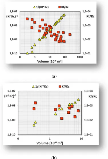
The two GFFs Kf and Kc provide useful insight into the core characteristics. The product KfKc is inversely proportional to the volume of the core, while the ratio Kf/Kc is a measure of the “stockiness” (large Ac area and/or small WA area) of the core. Figure 2.2 show the plots of 1/(KfKc) and Kf/Kc vs the volume, respectively for a set of F material MAGNETICs EE cores (a) [23] and 3C94 material FERROXCUBE EE/EI planar cores (b) [24]. Each core is identified by a couple of vertically aligned square and triangle
markers. In Figures 2.2(a)(b), bigger cores correspond to markers located towards the bottom-left corner of the plot area while stockier cores correspond to markers located towards the bottom-right corner of the plot area. The plot shows that cores having quite different form factor Kf/Kc may have the same volume, while cores having quite different volume may have the same form factor Kf/Kc. Given a certain value of the KfKc product, a core with higher Kf and lower Kc may involve higher core losses and lower copper losses than a core having the same KfKc product (same volume) with lower Kf and higher Kc.
(a)
(b)
Figure 2.2 Geometric form factors of: (a) EE MAGNETICs cores, (b) EE/EI planar FERROXCUBE cores.
Chapter 2. Transformer Design for Isolated Converters 25 Given nM, if the geometric constant Kf of a core is lower than the value Kf,max given by (32), then the total losses of the transformer designed with that core will certainly be lower than Ptot,max. Therefore, minimizing the transformer size means to find the value of nM allowing to make equation (32) fulfilled by the core having the biggest possible KfKc product. The minimum value of nM, required to prevent core saturation is obtained by solving (33):
2 T oM dc ac dc sat c M i V B B B B A n V D λ + = + < (33) which provides:
(
)
,min 2 T oM M sat c i sat dc V n round A V D B B λ = − (34)The Kf-Kc-based transformer design flow works as follows:
step #1 take cores of the preferred manufacturer, material and shape;
step #2 calculate GFFs Kf and Kc;
step #3 calculate Kf,max for each core, with nM ≥max{1,nM,minsat};
step #4 take the core having Kf ≤ Kf,max and maximum KfKc product.
Thus, no iterations and no verifications of physical reliability, loss budget compliance and core saturation are required. It should be noted that, although the previous design flow has been put in form of a sequence of steps, no code programming at all is required to apply the Kf-Kc-based method. All data, formulas and plots can be easily implemented using well known popular spreadsheets, as done for the dc-dc forward converter examples, illustrated in next paragraph.
2.4 Design Examples
A first example considered to illustrate the application of the Kf-Kc -based transformer design method is related to a dc-dc multi-output active-clamp forward converter with 48V input voltage and seven outputs (case a), whose voltage and current specifications are given in Table I.