A. Di Vito, A. Di Carlo, and M. Auf der Maur∗
Department of Electronics Engineering, University of Rome Tor Vergata, Via del Politecnico 1, 00133 Rome, Italy
A. Pecchia
CNR-ISMN, Via Salaria Km 29.300, 00017 Monterotondo (Rome), Italy
Carrier localization due to statistical fluctuations in Indium Gallium Nitride alloys has been recognized to play an important role for light emitting diode performance, both experimentally and through theoretical studies. While usually a random alloy assumption is made, in this work we take into account the presence of spatial nonuniformities in the indium content on the nanometer scale, and we theoretically analyze its impact on the electronic and optical properties of the alloy and the device. We show that indium clustering induces tail states in both the conduction and valence bands. This causes a reduction of the band gap and a broadening of the optical absorption edge. Furthermore, compositional fluctuations in the active region of the device determine a substantial broadening of the optical emission spectrum and a decrease of the peak emission energy, in agreement with experimental results. Moreover, the radiative recombination coefficient increases for increasing degree of clustering, suggesting a transition to a quantum dot like structure. Finally, the temperature dependence of the radiative coefficient derived for the nonuniform structures is in good agreement with the experimental results, that show a temperature behavior opposite to the trend expected from standard theoretical considerations.
I. INTRODUCTION
Indium Gallium Nitride is a successful material for the realization of efficient short-wavelength commercial light emitting diodes (LEDs) [1–3]. As a matter of fact, InGaN potentially covers the whole visible spectrum, thus allow-ing in principle to eliminate the phosphor based down conversion and enabling a color mixing approach, which would allow to further increase overall white LED effi-ciency [4].
Although the technology for InGaN based blue and white LEDs has been successfully commercialized, there are several material related issues, such as efficiency droop, green gap, compositional nonuniformity and spa-tial localization of carriers, which are still under debate [5–11]. While structural characterisation reveals a com-positional uniformity compatible with the assumption of a random alloy in high quality structures [12], one should expect some deviation from such an idealized structure on the atomic scale. Previous studies show that the fluc-tuations in the local indium concentration, even in the case of a uniform random alloy, lead to translational sym-metry breaking and carrier spatial localization [13–18]. Interestingly, the hole localization, particularly evident in samples containing indium clusters, appears to have a strong influence on the alloy properties [19, 20].
In most of the studies conducted so far, the impact of deviations from a uniform random alloy on the properties of InGaN has not been discussed [7, 8, 13, 14, 21, 22]. Furthermore, the theoretical analysis based on density functional theory (DFT) performed on clustered InGaN bulk structures [23, 24] lack a properly large supercell size
and a sufficiently large number of random samples. Thus, a discussion of the role of clustering for the properties of InGaN alloys and the performances of InGaN based LEDs, supported by a proper statistical characterization of the samples, is still needed.
In the present work, we theoretically describe the opti-cal properties of bulk InGaN alloys and InGaN/GaN sin-gle quantum well (SQW) LEDs, taking into account the statistical fluctuation of the alloy composition and the presence of indium clusters. In particular, we study the transition from a perfect random alloy towards a nonuni-form one. In Sec. II we present the theoretical approach used to perform the simulations and we describe in de-tail the method employed to generate the samples with several amounts of nonuniformity. The results of the sim-ulations are shown in Sec. III A and Sec. III B for the bulk material and the device, respectively. We analyze the outcomes of our study and compare them with the ex-perimental measurements, in terms of energy gap, optical absorption coefficient, emission spectra and temperature dependence of the radiative coefficient. We discuss the influence of compositional nonuniformity on the optical properties of both the bulk alloy and the device.
II. THEORETICAL APPROACH
In order to theoretically study the effect of alloy nonuniformity on macroscopic device performance we use a computational scheme combining continuum and atomistic models. To obtain the electronic and optical properties of both the bulk material and the device, we use an atomistic empirical tight binding (ETB) approach [25, 26]. The atomistic structures are first relaxed using a Keating valence force field (VFF) method [27]. The parameters α and β of the model are computed to
re-produce the bulk elasticity tensor of the pure materials. In the random alloy, for each In-N and Ga-N bond, we use the corresponding bulk values for α and β. Then, we compute the electron and hole states from which we cal-culate the momentum matrix elements, optical spectra and density of states.
For the simulations of the bulk material, we compute the first twelve electron and twenty-four hole states at the Γ point of the Brillouin zone. We use 10 × 10 × 10 nm3 periodic supercells with a mean indium
con-tent of x = 20%, corresponding to a value laying in be-tween those needed to obtain blue and green quantum well light emitting diodes. The qualitative results and trends demonstrated in this study, though, are valid for the whole range of technologically relevant indium con-tent values.
The random alloy samples are generated by substi-tuting gallium atoms with indium atoms randomly, as-suming a spatially uniform substitution probability equal to the mean indium concentration. Differently, for the nonuniform alloy we first distribute uniformly a certain percentage of indium atoms, which we denote in the fol-lowing as the percentage of uniformity in order to iden-tify different structures. The remaining indium atoms are then distributed with a spatially varying probabil-ity as follows. We first pick randomly a gallium atom. Then we count the indium atoms around this gallium up to the second nearest cation site, and we calculate the substitution probability as the ratio of this number and the available cation sites, leading therefore to a spatial correlation. This is repeated until all necessary indium atoms are distributed. Note that the total number of in-dium atoms is always the same, in order to fix the mean indium content.
The degree of clustering can be controlled by the per-centage of uniformly distributed indium atoms, for which we use values of 100% (random alloy), 80%, 60% and 40% of the total number of indium atoms. The lower the per-centage, the more clustering can be expected. To obtain statistically significant results, we simulate 50 structures for the uniform random alloy configuration, as well as for the slightly clustered alloy (80% uniformity). For the other cases we use 100 random samples, since the sta-tistical variations are more pronounced for the strongly clustered samples.
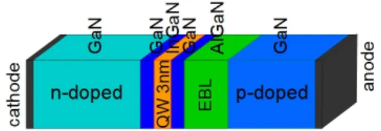
For the InGaN/GaN SQW LED we used a structure as shown schematically in Fig. 1, assuming a mean in-dium content of x = 20% and a well width of 3 nm. The considered device has the same structural parame-ters as those used for the calculations performed by Auf der Maur et al. [7]. As a matter of fact, the present work can be retained as an extension of the mentioned study, where the nonuniformity of the InGaN alloy was not addressed. Although spatial variations of the QW thickness can be expected in real LEDs, which influence device behavior as shown e.g. in [22, 28], we assumed here ideal QW inerfaces in order to not mix different ef-fects in our study. However, well width variations could
FIG. 1. Schematic view of the simulated structure.
be taken into account in our simulation model, using an approach similar to that in the analysis of Tanner et al. [22].
All simulations have been performed for a LED oper-ating point close to the maximum internal quantum effi-ciency, and a periodic supercell of 10×10 nm2 is chosen
in the quantum well plane. To obtain the electrostatic potential, needed to set up the tight-binding Hamilto-nian, and the quasi Fermi levels at the chosen operating point, we first solve the 1D Schr¨odinger/drift-diffusion problem, using TiberCAD software [29]. The potential is then projected onto the atomic positions, neglecting thus variations in the QW plane. For the calculation of the optical spectra, we compute the first eight electron and twelve hole states in the Γ, M , X and Y points of the reduced Brillouin zone, and we use the trapezoidal method for reciprocal space integration.
III. RESULTS AND DISCUSSION
In this section, we show the results of the simulations performed for the In0.2Ga0.8N alloy (Sec. III A) and the
InGaN/GaN SQW LED (Sec. III B), where the fluctua-tions of the indium content are taken into account. We analyze the outcomes of our theoretical derivation and discuss the comparison with the experimental measure-ments. We demonstrate that it is crucial to consider the presence of compositional nonuniformity in order to properly describe the optical properties of both the bulk material and the device.
A. Bulk In0.2Ga0.8N Alloy
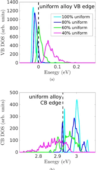
In Fig. 2 we show the mean density of states (DOS), i.e. the weighted sum of the DOS of all random sam-ples. We can clearly see that indium clustering yields tail states both in the conduction and valence bands and reduces the band gap by approximately 0.5 eV compared to the uniform alloy, confirming the results reported in previous studies [24, 30–32]. Moreover, the band gap val-ues calculated taking into account the nonuniformities of the samples are in reasonable agreement with the exper-imental data found in literature[33–35], as reported in Table I for completeness. Note that for the random alloy case only an insignificant broadening of the band edges is
(a)
(b)
FIG. 2. Density of states (sample average) for a bulk In0.2Ga0.8N alloy with several percentage of uniformly
dis-tributed indium atoms, resulting in several degrees of cluster-ing. The valence and conduction band states are represented in a) and b), respectively.
predicted. These band tails are due to the strong scatter-ing in the energies of the electron and hole ground states, which increases with increasing deviation from a uniform alloy. This effect is associated with increasing localiza-tion of the carrier wave funclocaliza-tions, which is correlated with the degree of indium clustering [36].
Concerning the optical properties of the clustered bulk In0.2Ga0.8N alloy, it is particularly interesting to analyze
the behavior of the absorption spectrum, shown in Fig. 3. We observe an increasing broadening of the optical absorption edge with increasing clustering degree, and washing out of a double peak structure at the absorption edge. This trends are in good agreement with the ex-perimental results reported by Butt´e et al. [37] on thick InGaN layers, at least under the reasonable assumption that growing indium content leads to increased nonuni-formity. Thus, the optical absorption edge broadening
TABLE I. Calculated and measured energy gap values. The theoretical results are reported for the uniform alloy and the structure with the highest clustering degree. The experimen-tal values #1, #2 and #3 refer to the studies of Wu et al. [33] (absorption measurements), Moret et al. [35] and Franssen et al. [34] (PL measurements), respectively.
Energy Gap [eV] this work 2.9−−−−−−→ 2.5clustering Exp#1 2.7 Exp#2 2.5 Exp#3 2.4
FIG. 3. Absorption coefficient (sample average) for a bulk In0.2Ga0.8N alloy with several percentage of uniformly
dis-tributed indium atoms, resulting in several degrees of cluster-ing.
observed by Butt´e et al. could be explained by increas-ing nonuniformity in the indium distribution.
B. InGaN/GaN SQW-LED
The mean emission spectra of the InGaN/GaN SQW LED are shown in Fig. 4 for each considered percent-age of uniformly distributed indium atoms. The band gap reduction, induced by the nonuniformity of the al-loy composition, yields a red-shift of the peak emission energy as the indium clustering degree increases. More-over, it can be seen that indium clustering induces a pronounced broadening of the spectrum. The measured emission spectrum of a SQW LED with a structure simi-lar to the simulated one but slightly lower indium content [38] is represented by the gray area in Fig. 4. Note that both the measured peak position and spectrum width are better described by the model with a nonuniform alloy. In particular, the case of 60% uniformity seems to reproduce rather well the experimental features. The high energy tail is well described, while the low energy tail shows slightly too little broadening. Note that the
FIG. 4. Calculated emission spectra (sample average) for an In0.2Ga0.8N quantum well at several percentage of uniformity.
The experimental spectrum [38] is depicted by the gray area.
60% uniform samples are consistent with the atom probe tomography (APT) measurements reported in literature [9, 28] if the limited APT detection efficiency is taken into account [39]. This is discussed in detail in Sec. I of the Supplemental Material [36], where we analyze the indium distribution within the In0.2Ga0.8N supercell for
all the considered percentage of uniformity.
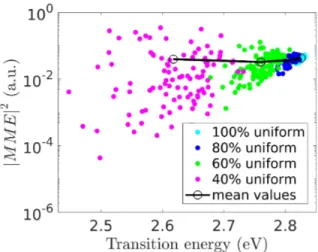
A scatter plot of the ground state momentum matrix elements (MME) evaluated at the Γ point of the Bril-louin zone for all the simulated structures and for each percentage of uniformity is shown in Fig. 5. It can be seen that the increase of clustering degree causes an in-creasing spread in the calculated MME values. This be-havior is due to the fact that the carriers’ localization induced by compositional fluctuations yields substantial statistical variations in the electron and hole wave func-tions overlap. This is illustrated in Fig. 6, where the ground state electron and hole wave functions for the structures with minimum and maximum MME are shown for the largest degree of clustering studied (40% of uni-formity). Furthermore, we can see in Fig. 5 that the MME average value slightly decreases for small nonuni-formity (up to 60% of uninonuni-formity) and then increases for the 40% uniform case. This is because, with substantial alloy nonuniformity, the indium clustering may localize both electrons and holes in the same spatial position, overcoming the quantum confined Stark effect (QCSE), as is the case in the left panel of Fig. 6. Indeed, in such a case the MME can be considerably larger than that of the random alloy. Otherwise, due to QCSE, the electron and hole states are influenced by the largely independent in-dium content fluctuations near the upper and lower QW interface, respectively[7].
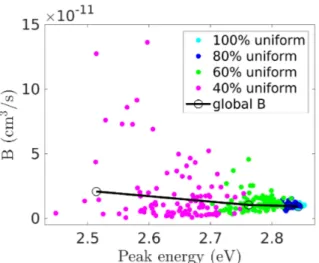
The radiative recombination coefficient B for all the simulated structures and each considered percentage of uniformity is shown in Fig. 7. The B value for each struc-ture is calculated assuming constant quasi Fermi levels
FIG. 5. Ground state transition MME, i.e. the MME related to the optical transition from the electron ground state to the hole ground state, of an In0.2Ga0.8N quantum well calculated
at Γ point for several percentage of uniformity. The results for each simulated sample are visualized as dots while the sample average is labeled by black circles.
FIG. 6. Ground state electron (red) and hole (yellow) wave functions for the In0.2Ga0.8N quantum well with 40%
(maximum clustering degree) of uniformly distributed indium atoms. Two structures are represented, corresponding to (right) the minimum and (left) the maximum value of MME. The isosurfaces containing 50% of the total ground state den-sity are shown. Indium, gallium and nitrogen atoms are de-picted in magenta, green and blue, respectively.
such that the mean carrier density is fixed and equal to ¯
n = ¯p = 5 × 1011 cm−2. The global radiative coefficient
is defined as ¯B = ¯Rr/(¯n¯p), where ¯Rr is the mean
ra-diative recombination rate, i.e. the weighted sum of the radiative recombination rate of all random samples[7]. As expected from the behavior of the MME, the indium clustering induces an increment of the spread in the cal-culated values of B. However, while the mean ground state transition MME decreases up to 60% of uniformity, the global value of the radiative coefficient increases for increasing nonuniformity. As a matter of fact, a higher number of optical transitions is allowed due to the
trans-FIG. 7. Radiative recombination coefficient B of an In0.2Ga0.8N quantum well for several percentage of
unifor-mity. The results for each simulated sample are visualized as dots and the global B is labeled by black circles.
lational symmetry breaking induced by the presence of disorder, as confirmed by the increase in the transitions related MME magnitude for increasing clustering degree [36]. Such an effect causes an increment of the radiative coefficient value when the nonuniformity of the structure increases. We could interpret the increase of the global B as the onset of the transition from QW to quantum dot like behavior, induced by the high degree of clustering, as suggested by the wave functions localization depicted in Fig. 6.
Finally, in order to obtain the temperature behavior of the radiative coefficient, we derived the occupation of the states using several values of temperature and adjust-ing the quasi Fermi levels so that the mean carrier den-sity is fixed. The temperature dependence of the global B so obtained is shown in Fig. 8 for several values of the mean carrier density. Only for the 100% uniform structure, the radiative coefficient ¯B decreases with in-creasing temperature for all the considered values of the mean carrier density. This is compatible with simple QW theory, which predicts B to be proportional to the in-verse of the temperature[40]. For increasing nonunifor-mity, the temperature dependence of ¯B becomes mostly constant or even increasing with temperature, in net trast with theory. In fact, when nonuniformities are con-sidered, strongly localized states are present that are lo-cated deeply inside the energy gap of the 100% uniform samples, as we discussed in Sec. III A. The MME re-lated to the low energy optical transitions between lo-calized states of nonuniform structures have lower values with respect to the MME associated to higher energy transitions, as shown in Figure 1 of Supplemental Ma-terial [36]. Thus, at low temperature, as the occupied states are mostly localized states, the radiative coefficient is lower with respect to the B value derived for higher temperatures, when the occupation of delocalized states
FIG. 8. Temperature dependence of B for an In0.2Ga0.8N
quantum well at several percentage of uniformly distributed indium atoms. The solid, dashed and dotted lines represent the values obtained for a mean carrier density of 1011, 5 × 10¹¹and 1012cm−2
, respectively. The experimental behavior [19] derived for a mean carrier density of approximately 1012 cm−2[41] is labeled by black circles. The results for the 40% uniform structure are not reported in the figure, since their range of variation is too wide and they are not interesting to compare with experiment.
becomes more important. Interestingly, this behaviour better matches the measured data presented by Nippert et al.[19] for a blue multi quantum well LED, presum-ably having slightly lower indium content, and reported in the figure by black circles. In particular, the experi-mental trend is very similar to the behavior predicted for the 60% uniform structure with ¯n = 5 × 1011cm−2. Note that we are considering the temperature dependence of B and not its magnitude, that clearly differs from experi-ment since the simulated device has not exactly the same structural parameters as those of the LED analyzed by Nippert et al.[19], so that in particular QCSE could be different.
IV. CONCLUSIONS
In conclusion, we considered the effect of small to mod-erate deviations from a random alloy structure on the optical properties of bulk In0.2Ga0.8N and InGaN/GaN
SQW LED. We found that, accounting for the nonunifor-mity of the alloy composition, band tails appear in the calculated DOS, inducing a reduction of the band gap energy and a broadening of the optical absorption edge, in agreement with the experimental results. In turn, the decrease of the band gap yields a lower peak emission energy of the LED device, as the clustering degree in-creases. Furthermore, the indium content fluctuations determine a substantial broadening of the LED’s optical emission spectrum. As a matter of fact, both the ex-perimental peak energy and width are better described
when alloy nonuniformity is taken into account. Never-theless, with our work we do not intend to rule out other mechanisms, such as excitonic effects, interface roughness [22, 42, 43], built-in field and local field effects [16, 44], which also lead to broadening and peak emission reduc-tion. Finally, when the presence of nonuniformity is con-sidered, a higher number of optical transitions is allowed due to the translational symmetry breaking induced by clusters. This causes the radiative coefficient to increase for increasing amount of clustering, suggesting a tran-sition to a quantum dot like structure. We found that the experimental temperature dependence of the
radia-tive coefficient can be well reproduced when assuming a nonuniform alloy. This is an interesting result, since the temperature behavior of B derived by standard theoreti-cal considerations is opposite to the experimental trend.
V. ACKNOWLEDGMENTS
This work has been supported by Horizon 2020 project ChipScope, under grant agreement number 737089.
[1] S. Nakamura, M. Senoh, and T. Mukai, P-GaN/n-InGaN/n-GaN double-heterostructure blue-light-emitting diodes, Japanese Journal of Applied Physics 32, L8 (1993).
[2] S. Nakamura, Present performance of InGaN-based blue/green/yellow LEDs, in Light-Emitting Diodes: Re-search, Manufacturing, and Applications, Vol. 3002 (In-ternational Society for Optics and Photonics, 1997) pp. 26–36.
[3] H.-M. Kim, Y.-H. Cho, H. Lee, S. I. Kim, S. R. Ryu, D. Y. Kim, T. W. Kang, and K. S. Chung, High-Brightness Light Emitting Diodes Using Dislocation-Free Indium Gallium Nitride/Gallium Nitride Multiquantum-Well Nanorod Arrays, Nano Letters 4, 1059 (2004). [4] H. S. El-Ghoroury, M. Yeh, J. C. Chen, X. Li, and C.-L.
Chuang, Growth of monolithic full-color GaN-based LED with intermediate carrier blocking layers, AIP Advances 6, 075316 (2016).
[5] E. Taylor, P. R. Edwards, and R. W. Martin, Colorime-try and efficiency of white LEDs: Spectral width depen-dence, physica status solidi (a) 209, 461 (2012). [6] J. Piprek, Efficiency droop in nitride-based light-emitting
diodes, physica status solidi (a) 207, 2217 (2010). [7] M. Auf der Maur, A. Pecchia, G. Penazzi, W. Rodrigues,
and A. Di Carlo, Efficiency drop in green InGaN/GaN light emitting diodes: The role of random alloy fluctua-tions, Phys. Rev. Lett. 116, 027401 (2016).
[8] C. M. Jones, C.-H. Teng, Q. Yan, P.-C. Ku, and E. Kioupakis, Impact of carrier localization on recombi-nation in InGaN quantum wells and the efficiency of ni-tride light-emitting diodes: Insights from theory and nu-merical simulations, Applied Physics Letters 111, 113501 (2017).
[9] M. J. Galtrey, R. A. Oliver, M. J. Kappers, C. J. Humphreys, D. J. Stokes, P. H. Clifton, and A. Cerezo, Three-dimensional atom probe studies of an InxGa1−xN/GaN multiple quantum well structure:
As-sessment of possible indium clustering, Applied Physics Letters 90, 061903 (2007).
[10] M. J. Galtrey, R. A. Oliver, M. J. Kappers, C. J. Humphreys, P. H. Clifton, A. Cerezo, and G. D. W. Smith, Response to Comment on Three-dimensional atom probe studies of an InxGa1−xN/GaN multiple
quantum well structure: assessment of possible indium clustering, Applied Physics Letters 91, 176102 (2007).
[11] J. A. Chan, J. Z. Liu, and A. Zunger, Bridging the gap between atomic microstructure and electronic properties of alloys: The case of (In,Ga)N, Phys. Rev. B 82, 045112 (2010).
[12] K. H. Baloch, A. C. Johnston-Peck, K. Kisslinger, E. A. Stach, and S. Gradeak, Revisiting the In-clustering ques-tion in InGaN through the use of aberraques-tion-corrected electron microscopy below the knock-on threshold, Ap-plied Physics Letters 102, 191910 (2013).
[13] T.-J. Yang, R. Shivaraman, J. S. Speck, and Y.-R. Wu, The influence of random indium alloy fluctuations in in-dium gallium nitride quantum wells on the device behav-ior, Journal of Applied Physics 116, 113104 (2014). [14] M. Lpez, A. Pecchia, M. Auf der Maur, F. Sacconi,
G. Penazzi, and A. Di Carlo, Atomistic simulations of InGaN/GaN random alloy quantum well LEDs, physica status solidi c 11, 632 (2014).
[15] P. R. C. Kent and A. Zunger, Carrier localization and the origin of luminescence in cubic InGaN alloys, Applied Physics Letters 79, 1977 (2001).
[16] M. A. Caro, S. Schulz, and E. P. O’Reilly, Theory of lo-cal electric polarization and its relation to internal strain: Impact on polarization potential and electronic proper-ties of group-III nitrides, Phys. Rev. B 88, 214103 (2013). [17] Z. Li, J. Kang, B. Wei Wang, H. Li, Y. Hsiang Weng, Y.-C. Lee, Z. Liu, X. Yi, Z. Chuan Feng, and G. Wang, Two distinct carrier localization in green light-emitting diodes with InGaN/GaN multiple quantum wells, Jour-nal of Applied Physics 115, 083112 (2014).
[18] S. Schulz, M. A. Caro, C. Coughlan, and E. P. O’Reilly, Atomistic analysis of the impact of alloy and well-width fluctuations on the electronic and optical properties of InGaN/GaN quantum wells, Phys. Rev. B 91, 035439 (2015).
[19] F. Nippert, S. Y. Karpov, G. Callsen, B. Galler, T. Kure, C. Nenstiel, M. R. Wagner, M. Straburg, H.-J. Lugauer, and A. Hoffmann, Temperature-dependent recombina-tion coefficients in InGaN light-emitting diodes: Hole lo-calization, Auger processes, and the green gap, Applied Physics Letters 109, 161103 (2016).
[20] B. Lee and L. W. Wang, Band gap bowing and electron localization of GaxIn1−xN, Journal of Applied Physics
100, 093717 (2006).
[21] D. Oriato and A. B. Walker, Effects of piezoelectric field, bias and indium fluctuations on a InGaNGaN sin-gle quantum well system, Physica B: Condensed
Mat-ter 314, 59 (2002), proceedings of the Twelfth InMat-terna- Interna-tional Conference on Nonequilib rium Carrier Dynamics in Semiconductors.
[22] D. S. P. Tanner, J. M. McMahon, and S. Schulz, Inter-face Roughness, Carrier Localization, and Wave Function Overlap in c-Plane (In, Ga)N/GaN Quantum Wells: In-terplay of Well Width, Alloy Microstructure, Structural Inhomogeneities, and Coulomb Effects, Phys. Rev. Ap-plied 10, 034027 (2018).
[23] X. Wu, E. J. Walter, A. M. Rappe, R. Car, and A. Sel-loni, Hybrid density functional calculations of the band gap of GaxIn1−xN, Phys. Rev. B 80, 115201 (2009).
[24] I. Gorczyca, S. P. Lepkowski, T. Suski, N. E. Christensen, and A. Svane, Influence of indium clustering on the band structure of semiconducting ternary and quaternary ni-tride alloys, Phys. Rev. B 80, 075202 (2009).
[25] J.-M. Jancu, R. Scholz, F. Beltram, and F. Bassani, Empirical spds∗tight-binding calculation for cubic semi-conductors: General method and material parameters, Phys. Rev. B 57, 6493 (1998).
[26] J.-M. Jancu, F. Bassani, F. D. Sala, and R. Scholz, Transferable tight-binding parametrization for the group-III nitrides, Applied Physics Letters 81, 4838 (2002). [27] D. Camacho and Y. Niquet, Application of Keating’s
va-lence force field model to non-ideal wurtzite materials, Physica E: Low-dimensional Systems and Nanostructures 42, 1361 (2010).
[28] D. Watson-Parris, M. J. Godfrey, P. Dawson, R. A. Oliver, M. J. Galtrey, M. J. Kappers, and C. J. Humphreys, Carrier localization mechanisms in InxGa1−xN/GaN quantum wells, Phys. Rev. B 83,
115321 (2011).
[29] TiberCAD simulation package, http://www.tibercad. org.
[30] L. Bellaiche, T. Mattila, L.-W. Wang, S.-H. Wei, and A. Zunger, Resonant hole localization and anomalous op-tical bowing in InGaN alloys, Applied Physics Letters 74, 1842 (1999).
[31] I. Gorczyca, T. Suski, N. E. Christensen, and A. Svane, Gap bowing in InxGa1xN and InxAl1xN under pressure,
physica status solidi c 6, S368 (2009).
[32] K. A. Mder and A. Zunger, Effects of atomic clustering on the optical properties of IIIV alloys, Applied Physics Letters 64, 2882 (1994).
[33] J. Wu, W. Walukiewicz, K. M. Yu, J. W. Ager, E. E. Haller, H. Lu, and W. J. Schaff, Small band gap bow-ing in In1xGaxN alloys, Applied Physics Letters 80, 4741
(2002).
[34] G. Franssen, I. Gorczyca, T. Suski, A. Kamiska, J. Pereiro, E. Muoz, E. Iliopoulos, A. Georgakilas, S. B.
Che, Y. Ishitani, A. Yoshikawa, N. E. Christensen, and A. Svane, Bowing of the band gap pressure coefficient in InxGa1xN alloys, Journal of Applied Physics 103, 033514
(2008).
[35] M. Moret, B. Gil, S. Ruffenach, O. Briot, C. Giesen, M. Heuken, S. Rushworth, T. Leese, and M. Succi, Op-tical, structural investigations and band-gap bowing pa-rameter of GaInN alloys, Journal of Crystal Growth 311, 2795 (2009), proceedings of the ”2nd International Sym-posium on Growth of III Nitrides.
[36] See Supplemental Material at, URL, for the analysis of the indium distribution within the samples and the de-scription of the clustering induced carrier localization and translational symmetry breaking.
[37] R. Butt´e, L. Lahourcade, T. K. Udavinys, G. Callsen, M. Mensi, M. Glauser, G. Rossbach, D. Martin, J.-F. Carlin, S. Marcinkeviius, and N. Grandjean, Optical ab-sorption edge broadening in thick InGaN layers: Random alloy atomic disorder and growth mode induced fluctua-tions, Applied Physics Letters 112, 032106 (2018). [38] M. Auf der Maur, B. Galler, I. Pietzonka, M. Strassburg,
H. Lugauer, and A. Di Carlo, Trap-assisted tunneling in InGaN/GaN single-quantum-well light-emitting diodes, Applied Physics Letters 105, 133504 (2014).
[39] L. Rigutti, L. Mancini, D. Hernndez-Maldonado, W. Lefebvre, E. Giraud, R. Butt, J. F. Carlin, N. Grand-jean, D. Blavette, and F. Vurpillot, Statistical correc-tion of atom probe tomography data of semiconductor alloys combined with optical spectroscopy: The case of Al0.25Ga0.75N, Journal of Applied Physics 119, 105704
(2016).
[40] P. K. Basu, Theory of optical processes in semiconduc-tors: bulk and microstructures, Vol. 4 (Clarendon press, 1997).
[41] As confirmed by personal communication of the author. [42] M. J. Galtrey, R. A. Oliver, M. J. Kappers, C. J. Humphreys, P. H. Clifton, D. Larson, D. W. Saxey, and A. Cerezo, Three-dimensional atom probe analysis of green- and blue-emitting InxGa1xNGaN multiple
quan-tum well structures, Journal of Applied Physics 104, 013524 (2008).
[43] C.-K. Tan, W. Sun, J. J. Wierer Jr, and N. Tansu, Effect of interface roughness on auger recombination in semiconductor quantum wells, AIP Advances 7, 035212 (2017).
[44] M. Baranowski, L. Janicki, M. Gladysiewicz, M. We lna, M. Latkowska, J. Misiewicz, L. Marona, D. Schiavon, P. Perlin, and R. Kudrawiec, Direct evidence of photo-luminescence broadening enhancement by local electric field fluctuations in polar InGaN/GaN quantum wells, Japanese Journal of Applied Physics 57, 020305 (2018).