Nanoscale
PAPER
Cite this:Nanoscale, 2019, 11, 6145
Received 11th January 2019, Accepted 4th March 2019 DOI: 10.1039/c9nr00343f rsc.li/nanoscale
Scanning tunneling microscopy and Raman
evidence of silicene nanosheets intercalated into
graphite surfaces at room temperature
†
I. Kupchak,
aF. Fabbri,
bM. De Crescenzi,
cM. Scarselli,
cM. Salvato,
cT. Delise,
cI. Berbezier,
dO. Pulci
cand P. Castrucci
*
cHighly oriented pyrolytic graphite (HOPG) is an inert substrate with a structural honeycomb lattice, well suited for the growth of a two-dimensional (2D) silicene layer. It was reported that when Si atoms are de-posited on the HOPG surface at room temperature, they arrange into two configurations: silicene nanosheets and three-dimensional clusters. In this work we demonstrate, by using scanning tunneling microscopy (STM) and Raman spectroscopy, that a third configuration stabilizes in the form of Si 2D nanosheets intercalated below thefirst top layer of carbon atoms. The Raman spectra reveal a structure located at 538 cm−1which we ascribe to the presence of sp2Si hybridization. Moreover, the silicon depo-sition induces several modifications in the graphite D and G Raman modes, which we interpret as experi-mental evidence of the intercalation of the silicene nanosheets. The Si atom intercalation at room tempera-ture takes place at the HOPG step edges and it detaches only the outermost graphite layer inducing a strong tensile strain mainly concentrated on the edges of the silicene nanosheets. Theoretical calculations of the structure and energetic viability of the silicene nanosheets and of the strain distribution on the outer-most graphite layer and its influence on the Raman resonances support the STM and Raman observations.
Introduction
Two-dimensional (2D) materials commonly possess unique optical bandgap structures, extremely strong light–matter interactions, and large specific surface area. Graphene, hexag-onal boron nitride (h-BN) and transition metal dichalcogen-ides (TMDs) have emerged as promising building blocks for novel nanoelectronics, providing a full range of material types, including large band gap insulators, semiconductors and semimetals.1 Among these 2D materials, silicene is gaining increasing interest for applications in nanoelectronics and spintronics.2
Differently from graphene, which is a one-atom thick carbon sheet with a honeycomb sp2configuration, silicon gen-erally takes tetravalence states like carbon in the diamond structure although it belongs to the same group as carbon in
the periodic table. In strong contrast with carbon, silicon tends to form an sp3 configuration with the surrounding silicon atoms in the solid phase. In fact, silicon atoms deposit on a solid surface agglomerate, even at very low coverages, and form a three-dimensional diamond-like structure with sp3 bonds.3,4In spite of these generally observed features, theore-tical studies have shown that there exists a metastable phase of single-layered silicon with a graphene-like structure, called silicene, either in a flat or slightly puckered configuration.5–8 The existence of this aggregation state has attracted much attention for the evident improvements that its use can imply in silicon based nano-electronic devices9 compared to gra-phene. Recently, some of us have reported evidence that patches of silicene can form on inert highly oriented pyrolytic graphite (HOPG).10,11 In these studies, scanning tunneling microscopy (STM) and ab initio molecular dynamics simu-lations revealed the growth of silicon nanosheets where the substrate/silicon interaction is minimized. STM measurements clearly display silicene nanosheets localized very close to small nanosized Si clusters leaving a large part of HOPG free of additional nanostructures. High resolution STM images show both the atomically resolved unit cell and the presence of a small buckling in the silicene honeycomb structure. In this paper we report evidence that for the same amount of silicon, deposited at room temperature, a third possibility exists, i.e. Si atom intercalation under the first graphitic sheet of HOPG.
†Electronic supplementary information (ESI) available. See DOI: 10.1039/ c9nr00343f
aV. E. Lashkaryov Institute of Semiconductor Physics, National Academy of Sciences
of Ukraine, Ukraine
bNEST, Scuola Normale Superiore, Istituto Nanoscienze-CNR, Pisa, 56127, Italy cDipartimento di Fisica, Università di Roma“Tor Vergata”, 00133 Roma, Italy.
E-mail: [email protected]; Tel: +39 06 72594545
dCNRS, Aix-Marseille Université, IM2NP, UMR 7334, Campus de St. Jérome, 13397
STM measurements show that an exchange of Si atoms occurs, involving from one to many atoms up to the formation of nanometric sized modulations of the flat HOPG surface (here-after called bubbles), thus decoupling the first HOPG layer from the substrate. Interestingly, these bubbles have a mound-like profile with an almost flat top, are monoatomically high and exhibit the same network and lattice periodicity of HOPG. All these observations support the formation of silicene nanosheets located underneath the first graphite layer of HOPG. Raman spectra reveal the presence of a feature located around 538 cm−1, which we assign to these silicene nanosheets.9,12,13 In addition, the silicon deposition induces several modifications to graphite D and G Raman modes. We interpret these modifications as clear experimental evidence of the intercalation of the silicene nanosheets which induces tensile strain on the overneath single graphite layer. Robust theoretical calculations of the structure and stability of the sili-cene nanosheets sandwiched among the outermost graphite layer and the graphite layers underneath support the experi-mental STM measurements. Raman calculations of the carbon G band confirmed that the G band presents a huge shift induced by the tensile strain. This is one of the first evidence of Si intercalation at room temperature in graphite substrates.
Experimental
A HOPG (from GE Advanced Ceramics, USA, 12 mm × 12 mm × 1 mm) sample was used as a substrate. A fresh surface of graphite was obtained by peeling the HOPG substrate with an adhesive tape and transferring it into an ultra-high vacuum (UHV) chamber. Silicon atoms were evaporated from a wafer (Sil’tronix ST, ρ = 1–10 Ω cm, n-doped) located 200 mm from the substrate. The deposition was achieved under UHV con-ditions (low base pressure of 10−10Torr) and at a constant rate of 0.1 nm min−1 (0.04 ML min−1) monitored by an Inficon quartz balance. Deposition was carried out keeping the sub-strate at room temperature (RT). STM imaging was performed using an Omicron-STM system with electrochemically etched tungsten tips. STM was calibrated by acquiring atomically resolved images of the bare HOPG surface. All images were acquired in the constant current mode and were unfiltered apart from the rigid plane subtraction. Ex situ Raman spec-troscopy and mapping have been performed without capping the sample. The Raman analysis was carried out with a 532 nm excitation laser, with a laser power density of 0.1 mWμm−2and an acquisition time of 1 s. The spectral resolution was 2 cm−1. The Raman system was a Renishaw InVia Qotor equipped with a confocal optical microscope and a high resolution Andor CCD camera. From the fitting of the Raman features by using Voigt curves, it is possible to evaluate the peak position, full width at half maximum (FWHM) and its associated error (0.5 cm−1). Theoretical approach
Theoretical calculations of the atomic structure of a silicon sheet under the first graphite layer have been performed using
density functional theory (DFT) within the generalized gradi-ent approximation (GGA) including van der Waals corrections in the form of a vdW-DF2 functional,14as implemented in the QUANTUM ESPRESSO software package.15 We have used Perdew–Burke–Ernzerhof (PBE)16pseudopotentials in a projector
augmented wave form. An integration of the Brillouin zone was performed using a 3 × 3 × 1Γ-centered grid of special points in the k-space, generated by the Monkhorst–Pack scheme17 and
Methfessel–Paxton smearing of 0.005 Ry.18 Convergence of the results was achieved with a 40 Ry cutoff in the wave functions and 160 Ry in the augmented charge density.
We modeled the HOPG sample by a three-layer slab of 12 × 12 graphene unit cells, with a vacuum layer of 2.0 nm thick-ness in the z-direction to separate the periodic images of the slabs. The atomic layers were relaxed until the Hellmann– Feynman forces became less than 10−3 a.u., keeping the bottom layer fixed. With regard to the Si atom layer under the top graphite layer of C-slab, we considered several size patches, consisting of a number of Si atoms from 1 to 37. In particular, for each number of Si atoms, we introduced them at the posi-tions corresponding to freestanding silicene sites. Then, we allowed the system energy to minimize and find the most stable structural arrangement. We found that for a small amount of Si-atoms (<24), the cluster tends to form a fcc(111) plane during the geometry optimization (data not shown here). However, starting from 24 atoms, the internal part of the Si-cluster pre-serves the initial, silicene-like structure, and such an atomic ordering is observed for the cluster with up to 37 Si-atoms. This is very different from the behavior of Si on Ag(111) where a pre-ferential flat structure of silicon was found for N < 24.19,20
Results and discussion
In Fig. 1 (central panel), we present the STM image of the HOPG surface exhibiting the atomic network typical of a graphite surface with some regions brighter than others. This has never been observed for the clean HOPG surface on extended nanometric terraces, while it appears soon after Si atom deposition. In the STM image it is possible to identify more brilliant areas involving one single atom, lines of atoms up to regions involving several atoms. By measuring the height of these brighter regions (see the line profiles in the top and bottom panels of Fig. 1), we observe that the most brilliant spots have a vertical distance from the HOPG basal plane of about 0.15 nm. Moreover, the atomic distance still remains the same as that of the HOPG lattice (i.e. about 0.25 nm). It is worth noting that if the Si atom was on top of the C atom in the HOPG network as predicted by Aktürk et al.,21 the line profile would be different from the one that we measured. In particular, we should have seen only one spot located at a higher distance from the C atoms of the graphite surface instead of the degrading heights of the surrounding atoms as shown in the reported line profile of Fig. 1.
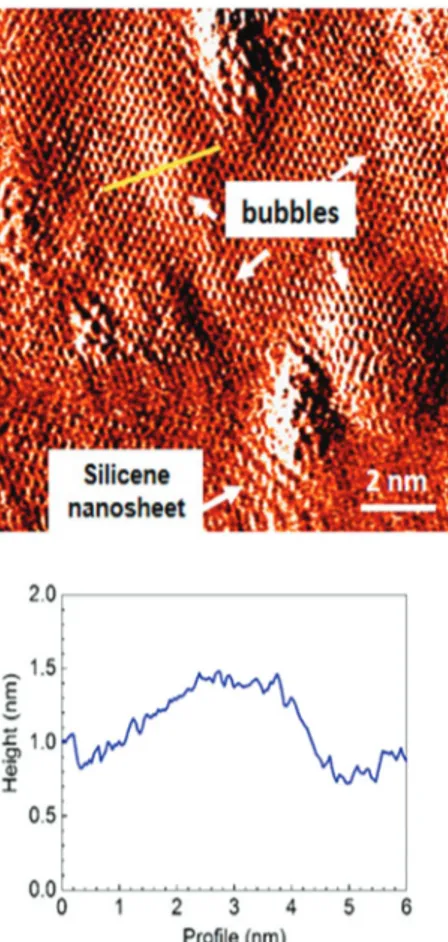
In the upper panel of Fig. 2, we present an STM image dis-playing the coexistence of three morphologies: Si clusters,
cene nanosheets and nanometer sized protrusions (bubbles) with an almost flat top as evidenced by the height profile pre-sented in the lower panel of Fig. 2. It would be interesting to estimate the percentage of each morphology. However, we do not have enough statistics to present such an evaluation, since to have atomic resolution on STM images and observe the Si arrangement types we need to scan very small sized regions (about 20 nm × 20 nm) and therefore we would need tens of STM images recorded on different regions.
In Fig. 3 a STM image taken at a higher spatial resolution shows the coexistence of a Si cluster and a bubble. A marked difference between the two regions is evidenced by the corres-ponding height profiles. The former (blue curve) shows a dis-tance between the atoms much larger than that typical of HOPG and a distance from the basal plane of about 1 nm. The atoms constituting the latter area (black curve) have a height distance of a few tenths of nanometer and maintain the HOPG atomic network. In addition, these last regions are almost flat at the top and rounded at the edges. This is particularly evident when reporting their height profile in the same x and y axis linear scale. The properties of Si clusters have been intensively investigated in the past, while no reports can be found on the presence and origin of such brilliant areas in Si/ graphite systems. A similar observation has been made in the case of silicon deposited on a MoS2 substrate kept at room
temperature.21 The authors interpreted their STM measure-ments in terms of Si intercalation under the first MoS2layers
forming a flat, bi-dimensional silicon cluster. However, there
are a number of studies showing that Si intercalation can occur only if the substrate is kept or annealed at temperatures higher than 800–900 K.23–27On the other hand, some
theore-tical calculations predict the energetic viability of silicene nanosheets sandwiched between two graphene layers occur-ring at room temperature.28 Several mechanisms have been suggested to explain how Si atoms penetrate a graphene layer. All of them indicate the occurrence of a sequence of Si–C atom position exchanges. In the case of a defect-free graphene layer, the energy barrier to be overcome is about 3 eV which is sup-plied to the Si atoms by a substrate temperature higher than 800–900 K.22,26However, the presence of defects in the
graph-ite outmost layer has been reported to lower the energy barrier for Si penetration,29thus suggesting the possibility of a Si–C atom exchange mechanism also at room temperature. An extended study of this intercalation mechanism is beyond the scope of the present paper. To shed light on the nature of the observed protrusions with an almost flat top on the HOPG surface, we performed Raman measurements.
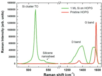
In Fig. 4, we present the Raman spectra recorded before and after Si deposition (red and green curves, respectively).
Fig. 1 Central panel: STM image (Itunn= 0.4 nA; Vbias= 0.3 V) of the
HOPG surface after 1 ML Si deposition at room temperature. Upper and lower panels: Height profiles of the brightest regions exhibiting a vertical distance from the HOPG basal plane of about 0.15 nm, while the planar distance between the spots remains the one typical of HOPG.
Fig. 2 Upper panel: STM image (Vbias = 0.3 V, Itunn= 0.4 nA) of an
extended area of the HOPG surface after the deposition of 1 ML of Si at room temperature. Lower panel: Height profile of the two-dimensional bubble indicated by the yellow line on the STM image. Note the almost flat top of such bubbles and the presence of the typical graphite network.
The Raman spectrum of the freshly cleaved HOPG curve is con-stituted by the D and G Raman modes, typical of a defective area, probably related to the edge of the HOPG terraces.30,31 The Raman spectrum after Si deposition is characterized by several resonances and the predominant feature, localized at 517 cm−1, originates from the transverse optical phonon of sp3 hybridized Si nanoclusters.10Close to this resonance, there is a small feature located at about 538 cm−1 (see Fig. 4 and Fig. S1 in the ESI†). This new Raman resonance is located very close to that reported by Castrucci et al., peaked at 542.5 cm−1 and ascribed to silicene formation on the HOPG surface.11
This suggests that, also in this case, Raman spectroscopy probes the typical atomic vibrations of a silicene layer. Interestingly, no Raman resonance has been detected around 800 cm−1, where silicon carbide modes are expected.32 This indicates that no Si–C interaction occurred upon Si deposition at room temperature on the HOPG substrate. In addition, as the opposite of what was shown by Castrucci et al.,11here a dramatic modification of the graphite Raman modes is present. The G and D bands widen as if they were composed of several contributions differently from those of clean HOPG. In particular, the G band presents components extending toward lower wavenumbers and the D band intensity domi-nates over the G band intensity. In order to clarify the effect of silicon intercalation, the Raman spectra are fitted with Voigt curves, and the obtained Raman peak parameters are pre-sented in Tables S1 and S2 of the ESI.† The Voigt analysis reveals the doubling of the D and G peaks, showing an additional peak for each mode. In Table S2 of the ESI† the parameters of the Raman modes of the sp3 silicon and sili-cene are presented. The D band fitting analysis shows the presence of two components ( presented in the ESI†) due to the contribution from the edges of graphite (high amount of defects).31For the G band, it is well known that it is extremely sensitive to strain in carbon nanotubes and graphene, owing to the phonon deformation caused by the change in the lattice constant.30
In order to understand the origin of such STM and Raman observations, we performed ab initio calculations to present a coherent interpretation of the experimental results. Fig. 5b shows the computed STM image, calculated within the
Fig. 3 Central panel: STM image (Itunn= 0.4 nA; Vbias= 0.3 V) of the
HOPG surface after 1 ML Si deposition at room temperature, showing two different morphologies: a three-dimensional Si cluster and a two-dimensional bubble. The heights of these features are very different as reported in the height profile shown in the top and lower panels. In the top panel, the distance dC–Cbetween two carbon atoms (0.25 nm) and
the larger distance between the Si atoms of the cluster are easily visible. In the lower panel, the observed network corresponds to that of HOPG.
Fig. 4 Raman spectra of the clean HOPG surface (red curve) and the HOPG surface after 1 ML Si deposition at room temperature (green curve). Note the presence of the TO resonance typical of three-dimen-sional sp3Si arrangement located at 517 cm−1and a new peak located at
538 cm−1which we ascribe to silicene intercalated under thefirst layer of graphene. The G and D band of HOPG are completely different from the ones of clean HOPG. These differences are discussed in the text in terms of strain experienced by the outermost graphene layer after sili-cene nanosheet intercalation and the presence of graphite edges.
Tersoff–Hamann approximation33after the insertion of one Si
atom under the first layer graphite slab. The theoretical current image is in good agreement with the experimental STM image of Fig. 5a. In fact, it is possible to observe both from the experimental and calculated images that the inser-tion of a single Si atom under the outmost graphite sheet pro-duces a strong increase of the current intensity of the C atom above the Si atom and a sizeable increase of the current inten-sity of the C atoms surrounding it. This is clearly shown in the line profile displayed in Fig. 1, bottom panel, where a marked decrease of the height occurs from the C atom located at the center toward the side C atoms. In addition, our calculations indicate that the single Si atom not only produces a bump in the upper graphite layer but also a depression in the layer underneath, as shown in Fig. 5c.
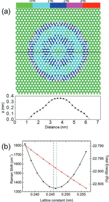
This effect is even more evident when we increase the number of Si atoms under the first graphite layer as shown in Fig. 6b and evidenced by the calculated line profile presented in Fig. 6c. We consider here a system consisting of a 12 × 12 × 3 C-slab with 37 Si-atoms inserted under the first C-layer. Although this system is very large and already contains 901 atoms, the top layer was detached from the slab during geome-try optimization. This means that a larger number of in-plane unit cells is required for such a number of Si-atoms. However, instead of increasing the size of the C-slab, we fixed one C-atom of the first layer (at the corner of the unit cell) to avoid the first layer detachment during the introduction of Si atoms. The 37 Si atoms were initially positioned as for an ideal free-standing silicene structure (i.e. honeycomb network) with a buckling between the nearest neighbor atoms of 0.042 nm.7,34
The resulting relaxed Si nanostructure has a typical silicene arrangement and remains located under the first graphite layer (see Fig. 6a). The corresponding theoretical height profile (see Fig. 6c) of the outermost graphite layer over the silicene
Fig. 5 (a) Blowup of the experimental STM image presented in the right-bottom part of Fig. 1. Notably, despite the different brightness, the atom–atom distance is always 0.25 nm, which corresponds to the graphite lattice parameter. (b) Ab initio theoretical calculation of the current image of one Si atom located underneath the outermost graph-ite layer of the HOPG substrate. The whgraph-ite solid and dot-dashed lines are guides for the eye that show the correspondence between the theoretical and experimental brightest C-atoms (only three over seven have been evidenced). (c) Sketch of the atomic vertical arrangement of the HOPG and Si atom profile as a result for the calculations. Note that the presence of the Si atom produces a bump in the upper graphite layer and a depression in the one underneath, involving not only the carbon atom located on top or under the Si atom but also a number of surrounding carbon atoms.
Fig. 6 Sketch of the planar (a) and vertical (b) arrangement of the Si and C atoms as results from the ab initio calculations for a system con-sisting of a 12 × 12 × 3 C-slab with 37 Si-atoms inserted under thefirst C-layer. Note that buckling of the nearest neighbour silicene atoms of 0.042 nm is present. (c) Theoretical height profile of the outermost graphite layer showing the effect induced by the silicene nanosheet. The height of the outermost graphite layer over the silicene nanostructure is about 0.15 nm, quite constant throughout the Si atom layer.
nanostructure is about 0.15 nm, quite constant throughout the Si atom layer (see the line profile in Fig. 6c). This is in very good agreement with the experimental results presented in Fig. 3. In addition, charge density calculation shows that no bonds are present between Si and C atoms (see Fig. 7). These calculations give hints of silicene nanostructure formation under the first graphite layer. This graphite outermost layer showing no bonds with the silicon underneath can be con-sidered as a graphene layer.
Fig. 8a presents the distribution of the calculated tensile strain of the C atoms on top of the silicene nanosheet. Different colors represent the percentage of strain, which varies between 0 to 4% of the C–C bond length of freestanding graphene. It is worth noting that the highest amount of strain is located close to the edge of the silicene nanosheet and at the most external border of the resulting bubble. Due to the low value of the strain, it is very hard to experimentally measure the variation in the C atom nearest neighbor distance with STM. However, these strain values have a dramatic effect on the vibration of the atoms and therefore on the corresponding Raman features. In Fig. 8b, we present the calculated graphene G band Raman shift (red point and curve) and the C–C atom total energy (black point and curve) as a function of the lattice parameter. The cal-culations were performed using density functional perturbation theory35 with a general set of parameters, used through the article, apart from the k-point grid that was selected to be 25 × 25 × 1. The green dashed line indicates the theoretical equili-brium lattice parameter of graphene, giving rise to a Raman shift equal to 1555 cm−1, whereas the blue dashed line marks the experimental lattice constant of graphene, giving in our cal-culations a Raman shift of 1578 cm−1, in fair agreement with the experiments (1588 cm−1). Within our model and parameters selected, this value appears to be greater than that observed experimentally. We performed a number of test calculations with higher wave-function cutoff and denser k-point grids, which showed us a better approach to the experimental value of the G line position, but had no effect on the dependence of the G-band position on the lattice constant. Therefore, we decided to proceed with the general parameter set to be coherent with the rest of the results. The calculations show that tensile strain, inducing a cell parameter larger than the equilibrium one, shifts the Raman position of the G band towards lower
wave-numbers. The major part of carbon atoms have a strain percen-tage between 1 and 2% which corresponds to a Raman down-shift of about 50 and 100 cm−1, respectively. This calculation allows one to account for the huge FWHM of about 100 cm−1of the experimental G band measured for the spectrum showing also the Raman feature located around 538 cm−1.
Fig. 8 (a) Distribution of the calculated tensile strain of the C atoms on top of the silicene nanosheet. Different colors represent the percentage of strain, which amounts to values between 0 to 4% of the C–C bond length of freestanding graphene. (b) Calculated graphene G band Raman shift (red point and curve) and the C–C atom total energy (black point and curve) as a function of the lattice parameter. The calculations were performed using density functional perturbation theory35with the general set of parameters, used through the article, and a k-point grid 25 × 25 × 1. The green dashed line indicates the theoretical graphene lattice parameter (a = 0.247 nm), and the blue dashed line indicates the experimental graphene lattice constant (a = 0.246 nm). The Raman shift at the experimental lattice constant is 1578 cm−1.
Fig. 7 Charge density calculation for a system consisting of a 12 × 12 × 3 C-slab with 37 Si-atoms inserted under thefirst C-layer. It shows that no bonds are present between Si and C atoms.
Conclusions
The joint theoretical and experimental study reported gives a new insight into the formation of silicene on HOPG. STM and Raman results show that at room temperature, Si atoms intercalate under the top graphite layer of the HOPG sub-strate. This phenomenon involves many Si atoms that nucle-ate in the form of silicene nanosheets. These sandwiched silicene 2D nanosheets do not interact with the top and bottom C layers. The Raman feature located at 538 cm−1 suggests the formation of silicene nanosheets. Correspondingly, the upper graphite layer experiences a large tensile strain which can reach 4%, producing dramatic changes in the G band as measured in the Raman spectrum. This is another fundamental piece of information in the highly debated and still open question of the synthesis, existence and stability of silicene on inert substrates.
Con
flicts of interest
There are no conflicts of interest to declare.
Acknowledgements
I. K., O. P., M. D. C., P. C., M. S. and M. S. would like to acknowledge the European Community for the HORIZON2020 MSC-RISE Project DiSetCom (GA823728). CPU time was granted by CINECA HPC center.
References
1 M.-Y. Li, C.-H. Chen, Y. Shi and L.-J. Li, Mater. Today, 2016, 19, 322–335.
2 J. Zhao, H. Liu, Z. Yu, R. Quhe, S. Zhou, Y. Wang, C.-C. Liu, H. Zhong, N. Han, J. Lu, Y. Yao and K. Wu, Prog. Mater. Sci., 2016,83, 24–151.
3 P. Scheier, B. Marsen, M. Lonfat, W.-D. Schneider and K. Sattler, Surf. Sci., 2000,458, 113–122.
4 E. J. Lautenschlanger and R. E. Martinez, Chem. Phys. Lett., 2001,341, 207–212.
5 P. Mélinon, P. Kéghélian, B. Prével, A. Perez, G. Guiraud, J. LeBrusq, J. Lermé, M. Pellarin and M. Broyer, J. Chem. Phys., 1997,107, 10278–10287.
6 Ş. Katircioglŭ and Ş. Erkoç, Phys. E, 2001, 9, 314–320.
7 S. Cahangirov, M. Topsakal, E. Akturk, H. Sahin and S. Ciraci, Phys. Rev. Lett., 2009,102, 236804.
8 P. Vogt, P. De Padova, C. Quaresima, J. Avila, E. Frantzeskakis, M. C. Asensio, A. Resta, B. Ealet and G. Le Lay, Phys. Rev. Lett., 2012,108, 155501.
9 L. Tao, E. Cinquanta, D. Chiappe, C. Grazianetti, M. Fanciulli, M. Dubey, A. Molle and D. Akinwande, Nat. Nanotechnol., 2015,10, 227–231.
10 M. De Crescenzi, I. Berbezier, M. Scarselli, P. Castrucci, M. Abbarchi, A. Ronda, F. Jardali, J. Park and H. Vach, ACS Nano, 2016,10, 11163–11171.
11 P. Castrucci, F. Fabbri, T. Delise, M. Scarselli, M. Salvato, S. Pascale, R. Francini, I. Berbezier, C. Lechner, F. Jardali, H. Vach and M. De Crescenzi, Nano Res., 2018,11, 5879– 5889.
12 J. Zhuang, X. Xu, Y. Du, K. Wu, L. Chen, W. Hao, J. Wang, W. K. Yeoh, X. Wang and S. X. Dou, Phys. Rev. B: Condens. Matter Mater. Phys., 2015,91, 161409(R).
13 D. Solonenko, O. D. Gordan, G. Le Lay, H. Sahin, S. Cahangirov, D. R. T. Zahn and P. Vogt, 2D Mater., 2016,4, 015008.
14 K. Lee, É. D. Murray, L. Kong, B. I. Lundqvist and D. C. Langreth, Phys. Rev. B: Condens. Matter Mater. Phys., 2010,82, 081101.
15 P. Giannozzi, O. Andreussi, T. Brumme, O. Bunau, M. Buongiorno Nardelli, M. Calandra, R. Car, C. Cavazzoni, D. Ceresoli, M. Cococcioni, N. Colonna, I. Carnimeo, A. Dal Corso, S. de Gironcoli, P. Delugas, R. A. Di Stasio Jr., A. Ferretti, A. Floris, G. Fratesi, G. Fugallo, R. Gebauer, U. Gerstmann, F. Giustino, T. Gorni, J. Jia, M. Kawamura, H.-Y. Ko, A. Kokalj, E. Küçükbenli, M. Lazzeri, M. Marsili, N. Marzari, F. Mauri, N. L. Nguyen, H.-V. Nguyen, A. Otero-de-la-Roza, L. Paulatto, S. Poncé, D. Rocca, R. Sabatini, B. Santra, M. Schlipf, A. P. Seitsonen, A. Smogunov, I. Timrov, T. Thonhauser, P. Umari, N. Vast, X. Wu and S. Baroni, J. Phys.: Condens. Matter, 2017,29, 465901. 16 J. P. Perdew, K. Burke and M. Ernzerhof, Phys. Rev. Lett.,
1996,77, 3865.
17 J. D. Pack and H. J. Monkhorst, Phys. Rev. B: Solid State, 1977,16, 1748.
18 M. Methfessel and A. T. Paxton, Phys. Rev. B: Condens. Matter Mater. Phys., 1989,40, 3616.
19 J. Gao and J. Zhao, Sci. Rep., 2012,2, 861.
20 C. Grazianetti, D. Chiappe, E. Cinquanta, M. Fanciulli and A. Molle, J. Phys.: Condens. Matter, 2015,27, 255005. 21 E. Aktürk, C. Ataca and S. Ciraci, Appl. Phys. Lett., 2010,96,
123112.
22 R. van Bremen, Q. Yao, S. Banerjee, D. Cakir, N. Oncel and H. J. W. Zandvliet, Beilstein J. Nanotechnol., 2017,8, 1952– 1960.
23 Y. Cui, J. Gao, L. Jin, J. Zhao, D. Tan, Q. Fu and X. Bao, Nano Res., 2012,5, 352–360.
24 F. Wang, K. Shepperd, J. Hicks, M. S. Nevius, H. Tinkey, A. Tejeda, A. Taleb-Ibrahimi, F. Bertran, P. Le Fèvre, D. B. Torrance, P. N. First, W. A. de Heer, A. A. Zakharov and E. H. Conrad, Phys. Rev. B: Condens. Matter Mater. Phys., 2012,85, 165449.
25 L. Meng, R. Wu, H. Zhou, G. Li, Y. Zhang, L. Li, Y. Wang and H.-J. Gao, Appl. Phys. Lett., 2012,100, 083101.
26 A. Visikovskiy, S.-I. Kimoto, T. Kajiwara, M. Yoshimura, T. Iimori, F. Komori and S. Tanaka, Phys. Rev. B: Condens. Matter Mater. Phys., 2016,94, 245421.
27 M. Neek-Amal, A. Sadeghi, G. R. Berdiyorov and F. M. Peeters, Appl. Phys. Lett., 2013,103, 261904.
28 G. R. Berdiyorov, M. Neek-Amal, F. M. Peeters and A. C. T. van Duin, Phys. Rev. B: Condens. Matter Mater. Phys., 2014,89, 024107.
29 G. Li, H. Zhou, L. Pan, Y. Zhang, L. Huang, W. Xu, S. Du, M. Ouyang, A. C. Ferrari and H.-J. Gao, J. Am. Chem. Soc., 2015,137, 7099.
30 A. C. Ferrari and D. M. Basko, Nat. Nanotechnol., 2013,8, 235. 31 A. C. Ferrari, Solid State Commun., 2007,143, 47–57.
32 S. Nakashima and H. Harima, Phys. Status Solidi A, 1997, 162, 39–64.
33 J. Tersoff and D. R. Hamann, Phys. Rev. B: Condens. Matter Mater. Phys., 1985,31, 805.
34 L. Matthes, O. Pulci and F. Bechstedt, J. Phys.: Condens. Matter, 2013,25, 395305.
35 S. Baroni, S. de Gironcoli, A. Dal Corso and P. Giannozzi, Rev. Mod. Phys., 2001,73, 515.