ALMA MATER STUDIORUM - UNIVERSIT `A DI BOLOGNA
ARCES - Advanced Research Center on Electronic Systems for Information and Communication Technologies E. De Castro
European doctorate program in Information Technology (EDITH) Cycle XX - ING-INF/01
TCAD Approaches to Multidimensional
Simulation of Advanced Semiconductor
Devices
Emanuele Baravelli
Ph.D. Thesis
Tutor Coordinator
Prof. Guido Masetti
Prof. Riccardo Rovatti
Contents
List of Symbols v
List of Figures vii
List of Tables xvii
Summary 1
Riassunto della tesi . . . 4 Acknowledgments . . . 8
I
Introduction - TCAD roadmap towards
in-creasing problem size
9
Technology progress trends . . . 11 Role of TCAD . . . 12 Increasing problem dimensionality in TCAD evolution . . . . 13 Motivations of this work . . . 16
II
Problem setting - Some TCAD roadblocks 19
1 Semiconductor device models 23
1.1 Drift-diffusion model . . . 23 1.1.1 Generation/recombination and mobility models . 24 1.1.2 Boundary conditions . . . 26 1.2 Hydrodynamic model . . . 27 1.3 Modeling quantum effects . . . 29
ii
2 First TCAD issue: problem discretization 31
2.1 Finite volume discretization . . . 31
2.2 Domain discretization . . . 33
2.2.1 Mesh requirements . . . 33
2.3 Adaptive meshing . . . 37
2.3.1 Review of the most common approaches to error detection . . . 38
2.3.2 Refinement-Solver interaction . . . 43
3 Second TCAD issue: variability estimation 45 3.1 Local variation sources: RD and LER . . . 46
3.2 Statistical characterization . . . 49
III
Proposed approaches - Multidisciplinarity
at the aid of TCAD
51
4 Wavelet-based approach to adaptive meshing 55 4.1 Wavelet analysis . . . 554.1.1 Continuous Wavelet Transform . . . 57
4.1.2 Localization property . . . 58
4.1.3 Characterization property . . . 59
4.1.4 Wavelet series . . . 61
4.1.5 Multiresolution approximation . . . 63
4.1.6 Discrete Wavelet Transform . . . 66
4.1.7 Multidimensional DWT . . . 68
4.2 Wavelet properties applied to mesh refinement . . . 70
4.3 Review of Wavelet approaches to device simulation . . . 73
4.4 The WAM approach . . . 74
4.4.1 Solve-refinement cycle . . . 75
4.5 WAM algorithm description . . . 76
4.5.1 Choice of the Wavelet functions . . . 76
4.5.2 1D WAM computation . . . 78
4.5.3 Algorithm for 2D domains . . . 79
iii
4.5.5 Dynamic mesh adaptation . . . 86
4.6 Mesh quality check procedure . . . 87
4.6.1 2D obtuse correction algorithm . . . 88
4.6.2 Correction procedure in three dimensions . . . 90
4.7 Implementation details . . . 92
4.7.1 WAM internals . . . 92
4.7.2 Validation cycle and user interface . . . 94
5 Statistical approaches to variability estimation 97 5.1 Monte Carlo approach for LER impact evaluation . . . . 98
5.1.1 Statistical models for LER . . . 98
5.1.2 Generation of the statistical ensemble . . . 99
5.1.3 Choice of representative parameters . . . 102
5.1.4 Statistical analysis of simulation results . . . 105
5.2 Techniques to improve the efficiency-accuracy trade-off . 106 5.2.1 Mismatch Evaluation . . . 106
5.2.2 The Half-Normal Statistics . . . 107
5.2.3 Exploiting Correlations . . . 108
5.3 Noise analysis for RD investigation . . . 113
5.3.1 Variability estimation technique . . . 114
IV
Applications - TCAD magnifying glass
117
6 Accurate physical insight through adaptive meshing 121 6.1 2D simulations . . . 1216.2 3D simulations . . . 127
6.3 Mesh quality . . . 132
6.4 Numerical considerations . . . 135
7 Impact of variability on future technology generations 139 7.1 Impact of LER on scaling of RDF and SDF FinFETs . . 140
7.2 Impact of LER on LSTP-32 nm FinFET technology . . . 145
7.2.1 Mismatch contributions from the fin-, top- and sidewall-gate-LER . . . 146
iv
7.2.2 Influence of doping profiles and number of fins . . 149 7.2.3 Correlation study . . . 153 7.3 LER requirements for circuit applications of FinFET . . 157 7.4 Impact of RD fluctuations on FinFET matching . . . 161
V
Conclusions
165
Bibliography 173
List of Symbols
C net ionized impurity concentration, defined as N+
D − NA−
Dn, Dp thermal diffusion coefficients for electrons and holes
~
E electric field
EC conduction band energy
EF Fermi energy level
EV valence band energy
Jn, Jp current densities for electrons and holes
N−
A ionized acceptor concentration
NC conduction band density of states
N+
D ionized donor concentration
R(ψ, n, p) net carrier generation/recombination
T lattice temperature
Tn, Tp electron and hole temperatures
αn, αp carrier ionization coefficients
² dielectric constant of the considered material
h Planck constant, 6.626 × 10⁻³⁴ J·s
¯h reduced Planck constant, defined as h/(2π)
kB Boltzmann constant, 1.381 × 10⁻²³ J/K
me, mh electron and hole effective masses
m density of states (DOS) mass
µn, µp electron and hole mobility
n electron concentration
nief f effective intrinsic carrier concentration
p hole concentration
ψ electrostatic potential
q elementary charge, 1.602 × 10⁻¹⁹ C
τn, τp carrier lifetimes
vn, vp drift carrier velocities
List of Figures
1 Hierarchical TCAD simulation flow. . . 14 2 Schematic representation of a FinFET device. . . 15 3 Handling 3D and 4D TCAD simulations enables circuit
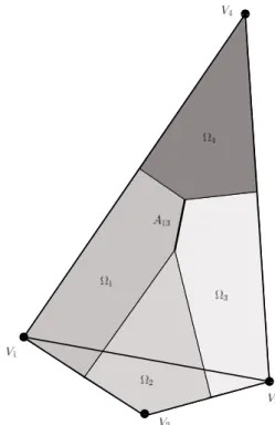
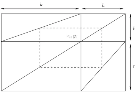
and system level analysis. . . 17 2.1 Voronoi tessellation of the domain. Ωi is the Voronoi
cell associated to mesh node Vi. lij is the length of the
mesh edge connecting nodes Vi and Vj, while dij is the
length of the Voronoi cell side normal to this edge (in 3D domains, this side is a facet whose area is Dij). . . 32
2.2 Example of adverse 2D Voronoi boxes due to obtuse an-gles. Fluxes between nodes V1 an V3are discretized using
area A13, which is far from the mesh line V1− V3. . . 35
2.3 Reference mesh structure for the computation of LTEs (2.5), (2.6). . . 41 4.1 Examples of Wavelet functions ψ(x). . . 57 4.2 Basis functions resulting from translation and dilation of
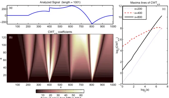
one of the mother Wavelets shown in Fig. 4.1. . . 58 4.3 CWT of a sample signal. The pixel intensity represents
the modulus of Wavelet coefficients for a certain position
b (abscissa value) at a given scale a (ordinate). Strong
gradients and singularities can be localized following lo-cal maxima across the slo-cale-translation plane. The cone of influence of a sharp region occurring around x = v is located in the space-scale plane where ψa,b intercepts v. . 60
viii List of Figures
4.4 (a) Sample signal. (b) Continuous Wavelet Transform. (c) Logarithmic plot of Wavelet coefficient maxima around
x = 200, 400, 800 as a function of the scale parameter. . 62
4.5 (a) Analyzed signal f ∈ C2(R). (b) WS coefficients
cor-responding to non-overlapping Ij,k supports. The mother
Wavelet is Daubechies2 (2 vanishing moments). (c)-(f)
f00 and coefficients at different resolution levels, scaled
with factor Kj = maxk|dj,k/f00|). (g) log2(Kj) plotted
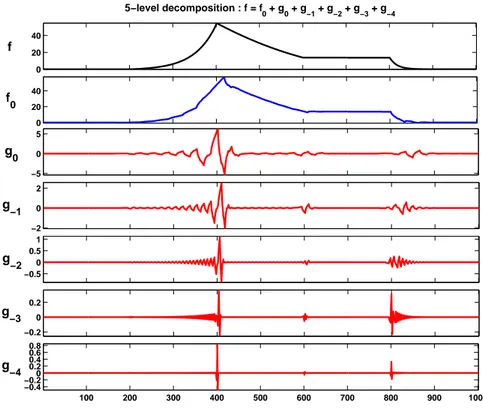
as a function of j. . . . 64 4.6 Multiscale decomposition of a sample signal f .
Approx-imation f0 is obtained after subtracting details gj at five
resolution levels. . . 65 4.7 Computational structure of the Discrete Wavelet
Trans-form. g[n] and h[n] are the low-pass and high-pass FIR filters used to calculate approximation and details, re-spectively. . . 67 4.8 2D DWT decomposition: H, G are the high-pass and
low-pass filters, respectively. Starting from approxima-tions at level j, they produce approximation (A) and detail (D) coefficients at level j + 1. . . 69 4.9 Two-dimensional Wavelet Transforms: the input matrix
is decomposed into four components (a). Then the al-gorithm can be iterated just on the low pass component GG (square two-dimensional transform - case b); other-wise, the signal may be decomposed with an anisotropic basis (rectangular two-dimensional transform - case c) . 70 4.10 Validation tool block diagram for the proposed
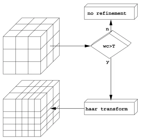
multires-olution analysis. . . 75 4.11 The solution on the sparse grid is convolved with the
Wavelet filter h[0−3]; if the resulting coefficient is greater than threshold η, a dyadic refinement is imposed. . . 78 4.12 Uniform (A) or anisotropic (B, C) refinement of a 2D
List of Figures ix
4.13 Anisotropic refinement of a prototype MOSFET device. Grid density is progressively increased under the gate and in the drain junction region. . . 81 4.14 3D Wavelet coefficients calculation. LPF and HPF are
the averaging and high pass 4-taps Daubechies filters [64], respectively. Directional details DX, DY and DZ can be calculated by alternated application of these filters in different directions. . . 82 4.15 (a) 3D uniform dyadic refinement. (b) Anisotropic
re-finement: while the strategy in [sse06] introduces new prismatic stencils, the alternative approach [tcad07] adds smaller 2-dimensional supports. . . 83 4.16 Examples of 3D, 2D and 1D db2 supports introduced by
the decoupled anisotropic refinement. . . 83 4.17 Details of two-step Wavelet refinement. The Wavelet
co-efficient is calculated convolving 43 samples of the
com-putational grid. A further step based on the Haar Trans-form is added to the algorithm to keep the number of inserted nodes as small as possible. . . 84 4.18 Haar analysis of a 3D db2 support in the x direction:
the stencil is split into three portions S1, S2, S3 and the average Haar coefficient is calculated for each of them. Ratios between the resulting values discriminate if S1 or
S3 can be excluded from the refinement. . . 85
4.19 Possible undesired patterns after triangulation of the re-fined grid. In particular (a) is simply a hole in the mesh (not necessarily including angles greater than 90 degrees), while (b) is an obtuse triangle. (a1) and (b1) show the correction procedure for these patterns. . . 89 4.20 Obtuse triangle with no axis-aligned edges (c), and
x List of Figures
4.21 Mesh changes produced by the obtuse triangle correc-tion. The inset shows identification and correction of one of the wrong patterns. The dashed blue segments are mesh edges before the correction, Steiner points are marked with squares and solid green lines represent the mesh after the verification step. . . 91 4.22 Examples of undesired mesh patterns (a) and quality
improvement through the 3D quality check procedure (b) during mesh refinement of a MOSFET driver. . . 92 4.23 Block diagram of the system integration software. The
first two blocks are the only steps requiring user interac-tion. Light-blue modules represent the filters that con-trol the solve-refine cycle and allow interfacing of the heterogeneous blocks MESH, SOLVE, WAM and VERIFY OBT. 95 5.1 Spectral densities corresponding to the Gaussian and
ex-ponential autocorrelation functions (∆ = 1.5 nm, Λ = 20 nm) typically used to model LER statistics. The Gaus-sian model only accounts for low spatial frequency com-ponents, while the exponential includes a wider spec-trum. A zoomed view of low-frequency spectral compo-nents is provided in the inset. . . 100 5.2 3D FinFET instance (a) and generated structures with
fin-LER (b), top-gate LER (d) and sidewall-gate LER (c).101 5.3 Simulated circuit for the estimation of MOSFET/FinFET
PDP through relations (5.4), assuming Cref = 1 fF. . . . 103
5.4 Butterfly curves in stand-by mode at Vdd = 1 V. SNM=min(SNM1,
SNM2), ∆SNM=SNM1-SNM2. . . 104
5.5 Schematic of a 6T SRAM cell. The highlighted zone corresponds to the relevant circuit in stand-by mode. . . 104 5.6 Histogram of current factor distribution for 85 3D
Fin-FET structures affected by sidewall-gate LER (see Fig. 5.2(b)). The Half-Normal fitting is also shown; peak position µ as well as left and right standard deviations (σL, σR) are
List of Figures xi
5.7 Example of linear correlation between structural and electrical parameters in a statistical ensemble of micro-scopically different devices. . . 110 5.8 Normal fitting of structural distribution x. . . 111 5.9 Variability estimation of p exploiting correlation to x.
Errors in σ values estimated through samples 1, N (“Method 1”) and 2, N −1 (“Method 2”) w.r.t. the value extracted from the full ensemble are also reported. . . 112 6.1 Simulated 2D diode (a) and MOSFET (b). . . 122 6.2 Comparison of I-V curves for the simulated 2D silicon
p-n diode with curved jup-nctiop-n. The WAM refip-nemep-nt
pro-vides a good match with reference characteristics when combined with the obtuse triangle correction: this step is essential to ensure accuracy and even to achieve con-vergence in the reverse bias. . . 123 6.3 WAM meshes for a 2D p-n junction breakdown simulation.124 6.4 nMOSFET Id(Vds) characteristics (Vgs = 0.7V , Vgs =
1.3V ). “ref. a” and “ref b” are the results obtained with two reference fixed meshes (5,000 and 10,000 points, respectively), while WAM data have been produced by the dynamical mesh adaptation (about 1,600 to 1,900 nodes). . . 125 6.5 nMOSFET Id(Vds) simulation with Vgs = 1.3V . . . 126
6.6 3D WAM anisotropic refinement of four different devices: (a) a 3D p-n diode, (b) and (c) power nMOS drivers, and (d) a FinFET device. . . 128 6.7 Mesh refinement of the p-n junction shown in Fig. 6.6(a)
through (a) an isotropic approach, (b) the naive 3D ex-tension of the WAM technique described in Sec. 4.5.3, and (c) the modified 3D WAM approach presented in Sec. 4.5.4. The same value of threshold η on Wavelet coefficients has been used in all three cases. . . 129
xii List of Figures
6.8 Impact of different refinement strategies on mesh size at various levels of Wavelet analysis for (a) the pn junc-tion, (b) the MOSFET driver of Fig. 6.6(b), and (c) the FinFET device. . . 130 6.9 Magnified view of mesh details for the MOSFET driver
in Fig. 6.6(b). Here, electron current density resulting from a simulation step at V gs = 1.3V , V ds = 1.78V is displayed. . . 130 6.10 Comparison of IV simulations with WAM (stars) and a
reference (solid line) fixed mesh for a the 3D p-n diode. WAM is launched with a fully adaptive mesh strategy i.e. adapting the mesh at each bias step. . . 131 6.11 Meshes produced by WAM during the sweep simulation
reported in Fig. 6.10: (a) V a = −7.375V , (b) V a = 0.1V . 132 6.12 Details of the mesh generated by WAM for the 3D
Fin-FET test structure in Fig. 6.6(d). . . 133 6.13 Mesh zoom in the FinFET channel region. . . 133 6.14 Comparison of Id-V gs curves for the test structure at
V ds = 0.05V . The WAM-generated mesh (about 17, 700
points) provides a good match with the results obtained with the reference mesh (about 47, 500 points). . . 134 6.15 Mesh quality in terms of maximum volume ratio of
ad-jacent elements (a), (b) and maximum number of ele-ments with a common node (c), (d) for the two drivers in Figs. 6.6(b) and (c) (here indicated as “driver 1” and “driver 2”, respectively). . . 135 6.16 Example of threshold influence on accuracy versus
num-ber of nodes for drain current in a 2D n-channel MOS. ηψ
and ηn,pare thresholds on electrostatic potential and
car-rier concentrations, respectively. Threshold values are given in relative terms (see Sec. 4.7.2). . . 136
List of Figures xiii
6.17 Influence of the threshold value on number of nodes (a) and accuracy (b) for a 3D p-n diode simulation (η1 <
η2 < η3). An extremely refined reference mesh was used
to compute errors. . . 137 7.1 SEM image of a Si-fin with (a) uncorrelated and (b)
correlated LERs, corresponding to resist- and spacer-defined fin patterning, respectively (IMEC data). . . 141 7.2 Line-width roughness (LWR) measurements for
resist-and spacer-defined fins (IMEC data). . . 141 7.3 Instances of simulated FinFETs affected by fin-LER
with-out (a) and with (b) phase correlation and by gate-LER (c). Nominal device dimensions are Wf in = 25 nm,
Lgate= 60 nm. . . 142
7.4 Independent contributions to mismatch in threshold volt-age (top) and current factor (bottom) for the FinFET ge-ometries shown in Table 7.1. Ensembles including about 200 devices were simulated. LER model: Gaussian au-tocorrelation function, ∆ = 1.5 nm, Λ = 20 nm. . . 143 7.5 IOF F vs. ION distributions for three of the four simulated
geometries. Off-current was extracted at Vgs = 0 V ,
Vds = 1 V and on-current at Vgs = Vds = 1 V . . . 144
7.6 Comparison of mismatch contributions from LER gener-ated through the Gaussian and the exponential models (∆ = 1.5 nm, Λ = 20 nm, ensemble size=200). . . 144 7.7 Doping profiles of the simulated n-type device (solid
lines) compared with those considered in Sec.7.1 (dashed lines). . . 146
xiv List of Figures
7.8 Mismatch in threshold voltage and current factor plotted as a function of the ensemble size ((a), (c)) and extracted from the full ensembles ((b), (d)). “F ”, “G top” and “G sw” are contributions to LER from the fin, top-gate and a single sidewall-gate, respectively; “G tot” is the total contribution to gate-LER estimated through (7.1) assuming statistical independence of individual compo-nents. . . 148 7.9 SEM cross-section of a multiple-fin FinFET (IMEC data).
One of the sidewall gates is highlighted and results of the edge detection are shown in the inset. . . 149 7.10 Impact of doping profiles on LER-induced mismatch:
extension concentrations Next ranging from 5 × 10¹⁸ to
1 × 1020 cm−3 have been considered. . . 150
7.11 Comparison between contributions to mismatch from the fin an top-gate roughness. (a), (c): impact of different extension concentrations Next. (b), (d): impact of
ex-tension slope xtsl. . . . 151 7.12 Parasitic resistance model of a FinFET. Gate-LER gives
rise to gate line-width-roughness, i.e. fluctuations in physical gate length and hence changes in channel resis-tance (Rch). Increasing extension profile concentration
and slope (junction engineering - see Fig. 7.10) reduces S/D resistances (RS, RD), thus enhancing the relative
importance of Rch. . . 151
7.13 Impact of extension concentration on relative importance of the top-gate-LER (σg) with respect to the fin-LER (σf).152
7.14 (a), (c): impact of fin- and top-gate-LER on mismatch of n- and p-type FinFETs. (b), (d): impact of fin-LER on mismatch of multi-fin devices. . . 153 7.15 Averaging operation for correlation analysis. (a): fin
width averaged over the whole fin length. (b): fin width averaged over the channel region. (c): sidewall-gate length averaged over the fin height. . . 154
List of Figures xv
7.16 Dependence of threshold voltage and current factor on the fin width averaged over the whole fin length((a), (d)), fin width averaged over the channel region ((b), (e)) and sidewall-gate length averaged over the fin height ((c), (f)). Slopes of the linear fits (S) are indicated in the figure.155 7.17 Percentage error of correlation-based variability
estima-tion with respect to results extracted from full ensembles, calculated for several datasets. . . 156 7.18 Comparison between VT-mismatch extracted from full
simulated distributions and exploiting correlation to hWf inich,
for multi-fin n-channel (a) and p-channel (b) devices. . . 157 7.19 Mismatch in threshold voltage and current factor as a
function of LER rms amplitude ∆ (a), (c) and correla-tion length Λ (b), (d), for typical ranges of measured values of these parameters respectively. Legends in the left plots show the slopes of linear fits. The maximum threshold voltage variability set by ITRS specifications is also plotted (dashed line). . . 158 7.20 6σ relative interval of ∆PDP versus number of fins for
stand-alone FinFETs (bars) and maximum circuit per-formance variability specifications for the ITRS 32 nm node (dashed line). . . 159 7.21 SNM and ∆SNM variability extracted from butterfly
curves (“Sim.”) in Fig. 7.22 and plotted as a function of the number of simulated SRAMs. . . 160 7.22 Measured (“RDF”, “SDF”) butterfly curves in
stand-by mode at Vdd = 1 V. Measured SRAM cell devices
(fabricated at IMEC) have Wf in = 30 nm, Lgate= 55 nm
and fin doubling for SDF; the total cell area is 6 µm2.
Simulations (“Sim.”) used to extract data for single-fin devices in Fig. 7.21 are also reported to provide an indication of the predicted spread at the LSTP-32 nm node due to the fin-LER contribution alone to variability. 161
xvi List of Figures
7.23 SNM (a) and ∆SNM (b) standard deviations extracted from simulated and measured butterfly curves shown in Fig. 7.22. . . 162 7.24 RD-induced threshold voltage and on-current percentage
variation as a function of the doping concentration in the channel ((a), (d)), S/D ((b), (e)) and extension regions ((c), (f)) of a n-type FinFET. Fin-LER contribution is also shown for comparison. . . 163
List of Tables
2.1 Values of geometry-related terms in eq. (2.2). . . 33 2.2 Expressions of physical parameters in eq. (2.2). B =
x/(ex − 1) is the Bernoulli function, while u and ρ are
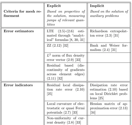
normalized potential and charge density, respectively. . . 33 2.3 Criteria for mesh refinement adopted in semiconductor
device simulation. . . 39 4.1 Filter bank coefficients g[n] and h[n] for the db2 scaling
function and Wavelet, respectively. . . 77 4.2 Filter bank coefficients g[n] and h[n] for the Haar scaling
function and Wavelet, respectively. . . 77 6.1 Simulated 2D diode and MOSFET: device description. . 122 7.1 Simulated device geometries (Wf in ' 0.42 × Lgate) . . . . 140
7.2 LSTP-32 nm FinFET specifications . . . 146 7.3 Statistical dependencies of LER contributions to
mis-match (σf: rough fin, σg: rough top-gate, σf +g:
com-bined fin- and top-gate-LER) . . . 147
Summary
Technology Computer-Aided Design (TCAD) is indicated by the In-ternational Technology Roadmap for Semiconductors (ITRS) as one of the enabling methodologies that can support advance of technology progress at the remarkable pace of Moore’s Law, by reducing develop-ment cycle times and costs in semiconductor industry. Several issues classified by the ITRS as difficult TCAD challenges can be seen as different implications of the same general trend, i.e. increasing prob-lem dimensionality. In fact, technology scaling increasingly emphasizes complexity and non-ideality of the electrical behavior of semiconductor devices and boosts interest on alternatives to the conventional planar MOSFET architecture. A three-dimensional representation is manda-tory to properly describe such devices: as a result, 3D simulations be-come a crucial need for everyday tasks. The outlined scenario highlights the need for meshing tools able to represent complex 3D geometries in an accurate yet efficient way, resolving all critical features of the de-vice structure without unacceptable drawbacks in terms of grid size. Automated gridding procedures are also desirable in process and de-vice simulations to provide a suitable mesh adaptation to geometry or solution changes while avoiding artifacts or spurious effects.
Predictive potentialities of TCAD also depend on its contribution to assessment and minimization of the impact of process variations, which get increasingly critical with device shrinking into the deca-nanometer range. Phenomena such as line-edge roughness (LER) and random dopant fluctuations (RD) broaden the device parameter distributions, thus requiring statistical treatment. This results in computationally challenging 4D problems, where the additional dimension is the size of
2 List of Tables
the considered ensemble.
The aim of this thesis is to present multi-disciplinary approaches to handle this increasing problem dimensionality in a numerical simula-tion perspective. In particular, the topic of adaptive meshing is tackled in a multiresolution framework which allows for an effective tracking of physical phenomena within two- and three-dimensional domains during quasi-stationary and transient simulations. The further dimensionality increase due to variability in extremely scaled devices is considered with reference to line-edge roughness and random dopant fluctuation issues. Statistical approaches to predict the impact of variability at an afford-able computational expense are proposed. Such techniques are then applied to address feasibility of the FinFET architecture as an alterna-tive to conventional CMOS technology for mainstream applications in sub-45 nm nodes.
The thesis is organized in five parts.
• Part I is a brief introduction to the parallel evolution of
technol-ogy and TCAD simulations, where the role of computer-aided de-sign and the increasing dimension of involved problems are high-lighted.
• In Part II, some of the main challenges for TCAD to successfully
deal with such problems are described, after illustrating the most common models used for semiconductor device simulation and the increasing complexity needed to describe aggressively scaled tech-nologies (Chapter 1). In particular, problem discretization issues are discussed in Chapter 2, where important mesh requirements for standard TCAD solvers are also described and conventional error detection approaches for mesh adaptation are introduced. The second considered TCAD challenge, i.e. variability estima-tion, is analyzed in Chapter 3, describing causes as well as mod-eling and characterization techniques available in literature for LER and RD.
• Approaches proposed in this thesis for tackling the two outlined
List of Tables 3
meshing for semiconductor device simulation is addressed in Chap-ter 4, presenting a new technique, based on mathematical tools and algorithms from the fields of multiresolution analysis and sig-nal processing. After providing the needed theoretical framework, the proposed approach is first introduced within a 2D setting; the extension to three-dimensional domains is then described, highlighting issues and solutions connected to dimensionality in-crease. A full integration of the developed C++ software into conventional TCAD environments is provided. Chapter 5 de-scribes the adopted approaches for variability estimation. Line-edge roughness is modeled through a Monte Carlo technique: en-sembles of microscopically different devices are generated by a Matlab program according to a proper statistical description of LER. Correlation analysis and other techniques to improve effi-ciency/accuracy of mismatch evaluation are discussed.
• Part IV shows how the proposed approaches help TCAD yielding
accurate physical insight and useful predictive results when deal-ing with multidimensional real-world applications. The Wavelet-based meshing technique is successfully applied in Chapter 6 to automatically generate and dynamically adapt computational grids for 2D and 3D devices including p-n diodes, MOSFET drivers with complicated geometries and FinFETs. Combining statistical simulations with experimental data, potentialities and shortcomings of the latter architecture are analyzed in Chap-ter 7. Different process options, such as resist-defined and spacer-defined fin patterning as well as junction doping, are taken into account to evaluate feasibility of FinFET technology for main-stream applications (e.g. SRAM) in future generation integrated circuits (ICs).
• Finally, conclusions and future perspectives of the work are
4 List of Tables
Riassunto della tesi
La progressiva contrazione delle dimensioni dei dispositivi a semicon-duttore ne rende sempre pi`u complesso e non-ideale il comportamento elettrico, alimentando inoltre l’interesse verso architetture alternative alla tecnologia MOSFET planare. Strumenti TCAD per la simulazio-ne di dispositivi elettronici avanzati sono fondamentali per l’analisi e lo sviluppo di nuove generazioni tecnologiche. D’altronde, la comples-sit`a della struttura e del funzionamento di tali dispositivi determina un progressivo aumento di dimensione dei problemi in esame, richiedendo sempre pi`u spesso una modellizzazione tridimensionale di applicazioni del mondo reale. In particolare, il compromesso tra accuratezza e onere computazionale delle simulazioni dipende fortemente dalla discretizza-zione del dominio. Inoltre, la dimensione del problema `e ulteriormen-te aumentata dalle variazioni di processo, che diventano sempre pi`u critiche in dispositivi deca-nanometrici. Fenomeni come rugosit`a geo-metriche (line-edge roughness, LER) e fluttuazioni casuali di drogaggio impongono la rappresentazione del singolo dispositivo come un insieme statistico di istanze microscopicamente differenti, dando luogo a difficili problemi quadri-dimensionali, in cui l’ulteriore dimensione `e data dalla cardinalit`a dell’insieme considerato.
Questa tesi si propone di utilizzare strumenti multidisciplinari per sviluppare approcci che permettano di gestire la crescente dimensiona-lit`a dei problemi di simulazione numerica. In particolare, verranno inve-stigati tecniche adattative per la generazione di griglie computazionali e metodi statistici per la stima di variabilit`a in dispositivi avanzati.
Il primo argomento verr`a affrontato proponendo un nuovo metodo (Wavelet-based Adaptive Method, WAM) per il raffinamento adattati-vo ed automatico della discretizzazione di domini 2D e 3D. Il software implementato fa uso di tecniche multirisoluzione basate sulla trasfor-mata Wavelet al fine di ottenere una stima di regolarit`a della soluzione. Ci`o permette di concentrare la risoluzione della griglia nelle regioni del dispositivo dove si manifestano i fenomeni fisici rilevanti, seguendone dinamicamente l’evoluzione al variare delle condizioni al contorno e
ga-List of Tables 5
rantendo la qualit`a delle mesh prodotte. In particolare, le principali caratteristiche di WAM possono essere riassunte come segue.
• Il software consente di sollevare l’operatore dal difficoltoso onere
di definire manualmente mesh adatte alla simulazione mediante volumi finiti di situazioni applicative del mondo reale: l’input richiesto `e infatti una griglia uniforme e molto sparsa.
• Il carattere direzionale delle informazioni fornite dall’analisi
Wa-velet permette di raffinare in maniera anisotropica le porzioni di dominio che richiedono una risoluzione elevata. Particolari ac-corgimenti sono stati messi a punto per mantenere una buona selettivit`a dell’algoritmo anche nel caso tridimensionale, garan-tendo cos`ı una notevole efficienza in termini di dimensioni della griglia.
• L’individuazione delle regioni sensibili sfrutta algoritmi di signal processing particolarmente efficienti.
• L’adattamento dinamico consente di gestire efficacemente
simu-lazioni quasistazionarie e in regime transitorio, incluse situazio-ni numericamente delicate come moltiplicazione a valanga dei portatori e breakdown.
• Grazie alla natura semiregolare delle griglie generate da WAM,
`e stato possibile definire una procedura di controllo della qualit`a della mesh in grado di identificare e rimuovere automaticamente configurazioni sfavorevoli per il solutore.
L’integrazione di WAM in un ambiente TCAD standard ne consen-te l’utilizzo per la simulazione di strutture 2D e 3D. Le applicazioni illustrate in questa tesi includono diodi, driver MOSFET con geome-trie articolate e dispositivi FinFET. Questi esempi mostrano l’efficacia e l’efficienza dell’algoritmo proposto rispetto a tecniche convenzionali note in letteratura, sia in termini di costo computazionale e propriet`a di convergenza della simulazione, sia per l’accuratezza e l’assenza di artefatti numerici nelle caratteristiche I-V prodotte.
6 List of Tables
Il problema dell’ulteriore aumento di dimensionalit`a dovuto a varia-zioni di processo `e stato affrontato con riferimento a due fenomeni che stanno acquisendo crescente importanza, quali il line-edge roughness (LER) e le fluttuazioni casuali di drogaggio. Questa attivit`a si inse-risce nell’ambito di una collaborazione con il centro di ricerca IMEC (BE), avviata durante un periodo di permanenza di sei mesi presso tale struttura. In particolare, in questa tesi sono descritti alcuni approcci statistici, che consentono di stimare la variabilit`a ad un costo com-putazionale accettabile. Con l’ausilio di tali strumenti, viene studiato l’impatto dei fenomeni citati su dispositivi FinFET, che costituiscono una promettente alternativa all’architettura CMOS planare. L’impiego di simulazioni TCAD 2D e 3D, in combinazione con dati sperimentali, ha permesso di valutare le prestazioni di matching della tecnologia Fin-FET, relativamente a singoli dispositivi e blocchi circuitali di base, co-me co-memorie statiche (SRAM), confrontando diverse opzioni di processo legate alla modalit`a di definizione della fin e ai profili di drogaggio.
In particolare, sono stati analizzati i contributi di mismatch dovuti alle rugosit`a della fin, del gate superiore e di quelli laterali, valutando la variabilit`a su insiemi statistici costituiti da numerose realizzazioni microscopicamente differenti. Queste simulazioni evidenziano un for-te impatto del line-edge roughness al nodo for-tecnologico LSTP-32 nm, quando i dispositivi FinFET potrebbero cominciare ad essere impie-gati su larga scala. Il contributo pi`u critico risulta quello dovuto alle rugosit`a della fin, definita mediante il processo di fabbricazione RDF (resist-defined fin patterning) comunemente adottato, che non d`a luogo ad alcuna correlazione tra la forma dei due bordi. Si mostrer`a, infatti, come tali rugosit`a influenzino il comportamento elettrico del dispositi-vo prevalentemente variando lo spessore medio della fin nella regione di canale. Similmente, l’impatto delle rugosit`a dei gate, sebbene di entit`a minore, `e principalmente legato alla variazione della lunghezza media dei rispettivi canali. Queste informazioni, risultanti da un’analisi di cor-relazione tra variabilit`a geometrica ed elettrica, possono essere sfruttate sia per ottenere stime di variabilit`a approssimate ad un costo computa-zionale estremamente ridotto, sia per la definizione di modelli compatti
List of Tables 7
utilizzabili ai livelli gerarchici superiori di simulazione TCAD. Diversi modelli statistici sono disponibili in letteratura per la descrizione del line-edge roughness; le simulazioni effettuate mostrano, per`o, come il contributo pi`u significativo al mismatch sia dovuto alle basse frequenze spaziali della rugosit`a, ben rappresentate dal modello ad autocorrela-zione gaussiana. Utilizzando per i parametri di questo modello i valori tipicamente estratti da misure sperimentali, si prevede che il LER pos-sa condizionare sensibilmente il funzionamento di celle SRAM al nodo tecnologico esaminato. Le fluttuazioni casuali di drogaggio, simulate mediante un approccio perturbativo, appaiono invece meno critiche in corrispondenza dei range di concentrazioni normalmente impiegati per la realizzazione di dispositivi FinFET.
Due possibilit`a sono state esplorate per minimizzare l’impatto del fin-LER su tali dispositivi. La prima consiste nell’impiego di strutture multi-fin: ci`o ha un effetto benefico sul matching dei parametri elet-trici, in accordo con la legge di Pelgrom. La seconda opzione consiste nella definizione della fin mediante un processo di tipo spacer-defined: oltre ad aumentare la densit`a di integrazione, tale tecnica d`a luogo ad una significativa correlazione tra i bordi della fin. Si prevede che questo possa determinare una notevole riduzione della variabilit`a elet-trica. I dati sperimentali riguardanti celle SRAM composte da FinFET realizzati con tale tecnologia, per`o, rivelano, allo stato attuale, una marcata instabilit`a del processo di fabbricazione, che dovrebbe dunque essere perfezionato. I progettisti dovranno prestare, inoltre, particolare attenzione all’ottimizzazione dei profili di drogaggio, poich´e le simula-zioni effettuate indicano un accentuarsi dei problemi di variabilit`a in corrispondenza dell’aumento di concentrazione nelle estensioni e della definizione di giunzioni il pi`u possibile brusche.
Combinando strumenti statistici con simulazioni TCAD, il lavoro svolto fornisce dunque indicazioni utili per lo sviluppo di applicazioni basate sull’architettura FinFET nelle prossime generazioni tecnologi-che.
8 List of Tables
Acknowledgments
I would like to gratefully acknowledge all the people who guided, ac-companied and supported me during my Ph.D. studies.
Many thanks to Prof. Guido Masetti, who gave me the opportunity to step into the world of research and continuously encouraged my walk. This walk would not have led anywhere without the patient guide and experienced advise of Nicol`o Speciale, who introduced and directed me on the fields of Wavelets and semiconductor device simulation.
Working in a team has been a wonderful and forming experience, not only from a scientific point of view, especially thanks to Luca De Marchi and Francesco Franz`e.
Thanks to Marco Messina, Salvatore Caporale and Alessandro Pal-ladini for their friendship and many valuable suggestions.
Words cannot properly express my gratitude to the faithful mate of all my studies, Nicola Testoni.
Finally, I would like to acknowledge Abhisek Dixit, Malgorzata Jurc-zak, Kristin De Meyer and the whole EMERALD team at the Inter-University Microelectronics Center (IMEC) for launching and support-ing me in the exploration of FinFET devices and process variations during my stay-abroad period in Belgium and afterwards.
Part I
Introduction
-TCAD roadmap towards
increasing problem size
11
“Everything should be made as simple as possible, but not simpler.” A. Einstein
Technology progress trends
Modern semiconductor technology has been developed after important inventions and discoveries achieved between 1945 and 1970. Starting from the fabrication of the first bipolar junction transistor in the late 1940s, the technology gradually improved until, in the 1960s, it reached a sufficient level of maturity for the production of good quality gate ox-ides. This allowed for the metal-oxide-semiconductor field effect tran-sistor (MOSFET) to be introduced and soon inserted into monolithic integrated circuits (ICs), thus giving birth to the CMOS technology era. In 1965, just a few years after the fabrication of the firs IC, Gordon Moore made his famous prediction that the number of transistors in an integrated circuit would double every year [1]. Updated in 1975 with a prospected density doubling rate of two years, the so-called “Moore’s law” has been describing the evolution of the semiconductor industry with extraordinary precision so far.
The reason for this exponential increase of chip complexity over time mainly lies in the continuous shrinking of device geometry, known as scaling. Since 1992, the Semiconductor Industry Association (SIA) has been providing essential research and development guidelines on the key needs for technology scaling to keep up with the exceptional rate outlined by Moore’s law. Initially elaborated on a national basis, such guidelines were periodically updated and gradually extended to in-clude worldwide industry contributions, resulting in a document called the “International Technology Roadmap for Semiconductors” (ITRS), first published in 1998. The document contains a 15-year outlook on the major trends of the semiconductor industry and provides clear re-search targets as well as possible solutions to emerging requirements
12
and issues, including forecasts on materials and software.
Role of TCAD
The progress of technology is so fast, that the underlying scientific un-derstanding has frequently proved to be inadequate, leaving wide room to empirical approaches. However, an accurate physical description is essential at various stages of IC design and fabrication as well as to sup-port innovation. In particular, computer simulations turn out to be the only way to investigate physical phenomena which cannot be directly studied through practical measurements. The synergistic combination of modeling and simulation tools, known as technology computer-aided design (TCAD), helps with the critical analysis and detailed under-standing at various levels, including
• system and circuit design • device engineering
• process development
• integration into manufacturing.
In fact, computer simulations allow investigating potentialities and physical limitations of manufacturing processes as well as developing
behavioral models at the transistor and circuit level of ICs [2]. This
is essential to the development of new technology generations, charac-terized by an increasing design complexity. Beside providing a deep
insight, especially for aggressively scaled devices, for which complex
physical phenomena and small dimensions severely limit the descriptive capabilities of measurements, TCAD simulations exhibit a remarkable
predictive valence upon calibration to proper experimental data [3, 4].
The generation of predictive models plays a crucial role in reducing development cycle times and costs in semiconductor industry. This role is highlighted by the 2005 edition of the ITRS [5], where TCAD is indicated as a crucial enabling methodology supporting technology progress.
13
However, several issues are presented in the ITRS as difficult TCAD challenges, that can be read as different symptoms of the same general trend, i.e. the increasing problem dimensionality. This comes as a consequence of scaling and has a twofold implication.
On the one hand, more and more complex device modeling is needed for computer simulations at the process and physical levels. This is due to geometry shrinking, which enhances the importance of a number of phenomena contributing to the device behavior; moreover, the intro-duction of new materials and architectures increasingly complicates the transistor structure. In addition, the difficult fabrication of very small features sizes brings about significant parametric variations.
On the other hand, design complexity is constantly enhanced by the increasing density of integration, which has led to a huge gap be-tween physical simulation on the nanometer-scale and IC design on a millimeter-scale featuring complexities up to 109 components. This
problem can only be tackled through a rigorous hierarchical approach to TCAD (see Fig. 1), in which process and device simulations provide informations for the development of compact models, suitable for cir-cuit and system level analysis. These informations include in the first place accurate SPICE-like parameters resulting from a realistic investi-gation of the device electrical behavior. In the second place, variations
of SPICE-like parameters must be carefully estimated to achieve
ac-ceptable model predictivity, including process yield evaluation.
The outlined dimensionality increase is evident in the historical evo-lution of TCAD, as described in the next Section.
Increasing problem dimensionality in TCAD
evolution
The first steps in computer simulations were drawn the late 1960s and 1970s, when one-dimensional (1D) approaches were generally suf-ficient to deal with bipolar technology and early MOSFET devices: 1D charge transport phenomena were predominant in these large, usually
14 Models Device Compact Parameter Extraction Parameter Extraction Characteristics Characteristics Measurements Measurements Models Compact Circuit Simulators Process Simulators Device Simulators Simulators Circuit System
Figure 1: Hierarchical TCAD simulation flow.
fractions of micrometers and channel lengths of several micrometers. Extrapolation of quasi-2D doping distributions from sets of 1D pro-files helped with process design optimization, although sheet resistances and minority carrier effects could not be predictively evaluated.
Starting from the 1980s, aggressive MOS scaling led to the very-large and ultra-very-large scale integration (VLSI and ULSI) eras based on CMOS technology. Fully-2D simulators soon became indispensable to model increasing process complexity and coupled physical effects, including local oxide isolation (LOCOS), dopant diffusion, subthreshold conduction, parasitic phenomena such as latchup and punchthrough.
The ever-shrinking transistor size led in the 1990s to a growing need for atomic-scale physics to correctly model the device behavior. Short/narrow channel effects and, later on, quantum effects such as gate leakage and carrier confinement required more and more sophis-ticated transport models, often amounting to several numerically stiff and highly non-linear coupled partial differential equations (PDEs). In addition, physical phenomena, including multi-device interactions,
15
Figure 2: Schematic representation of a FinFET device.
interconnect and substrate parasitics, reliability issues such as electro-static discharge (ESD), started to become inherently three-dimensional (3D).
The need for 3D simulation tools has become indispensable in the last years, when approaching scaling limits of bulk CMOS technology have boosted research on alternative, essentially three-dimensional ar-chitectures, e.g. Multiple-Gate devices (MuGFETs) [6, 7]. One of such devices is the FinFET schematically represented in Fig. 2. The silicon fin is surrounded by two sidewall gates and optionally by a top one, thus providing a better short-channel control. Charge transport is therefore a real 3D phenomenon, composed of two current flows parallel to the fin sidewalls and, optionally, an additional third one at the fin top.
The problem size in TCAD simulations is further increased by an-other major drawback of geometry scaling, i.e. enhanced process fluctu-ations. Although improved manufacturing tools have reduced absolute variability, relative variability in component geometries is becoming an increasing concern. Polysilicon/metal edge grains, photoresist edge
16
roughness, gate oxide thickness and permittivity non-uniformities are among the major sources of fluctuations. Moreover, charge transport in nanoscale devices is influenced by random distribution of dopant atoms in the channel. As a result, considerable fluctuations are seen in the device behavior, broadening the electrical parameters distribution and hence limiting IC performance. To take variability into account, each single device has to be represented by an entire distribution of struc-tures with random geometry and doping fluctuations. Not only a 3D description of each device instance is mandatory in most applications, but the full simulation space is transformed into a four-dimensional (4D) one: the additional dimension is given by the size of the consid-ered ensemble.
Motivations of this work
The dimensionality increase in TCAD problems and the enhanced com-plexity of the involved physical models give rise to the fundamental challenge of producing reasonably accurate and predictive results with an acceptable computational effort. In this thesis, two topics are ad-dressed, which have a key role in meeting such a challenge, namely meshing and variability estimation.
The lowest hierarchy levels of TCAD include description of physical characteristics and behavior of the single device. This implies solv-ing coupled PDEs which describe the evolution of either geometry and impurity distribution as a result of manufacturing process steps, or in-ternal physical quantities in response to electrical boundary conditions (BCs). Solutions to such problems can only be sought numerically; thus, a proper discretization procedure is required. Mesh generation is the discrete representation of the considered domain: this operation has a crucial impact on convergence, accuracy and efficiency of the sim-ulation. However, meshing “has become a major issue because device architectures are now essentially three-dimensional” (ITRS 2005 [5]), as also highlighted in the previous Section. Therefore, automatic grid generation and adaptation are highly desirable, both for improving the
17
Chip−level analysis Compact models Characterize device/process
Simulate process variations Simulate complex devices
Extract parameters
Handle 3D (meshing) Handle 4D (variability)
Extract parameter fluctuations
Figure 3: Handling 3D and 4D TCAD simulations enables circuit and system level analysis.
trade-off between computational complexity and solution accuracy, and for relieving TCAD users from a difficult and burdensome task. This motivates the investigation of adaptive meshing techniques for semi-conductor device simulation.
In addition to increasing complexity of the device structure and behavior, dimension shrinking collides with the intrinsic discreteness of charge and matter and with difficulties and tolerances in the fabrication process. Random dopant fluctuations and line-edge roughness are two sources of major concern for future technology nodes. Techniques for evaluating variability at an affordable computational cost are sought, which sets the stage for the second analyzed topic.
Approaches described in this thesis can boost feasibility of challeng-ing TCAD simulations and help with characterizchalleng-ing new processes and devices, such as FinFETs. As described in Fig. 3, this allows developing suitable circuit mismatch models, which can be used in predictive sim-ulations of circuit and system-level performance of new technologies.
Part II
Problem setting
-Some TCAD roadblocks
21
“That which is static and repetitive is boring. That which is dynamic and random is confusing. In between lies art.” J. A. Locke
In this Part, the topic of semiconductor device simulation is introduced, describing modeling and numerical aspects (Chapter 1). Issues related to the discretization of the simulation domain are highlighted, which result in stringent mesh requirements. Consequent difficulties in the mesh generation task represent a challenging TCAD “roadblock” that calls for automatic and adaptive techniques, as discussed in Chapter 2. The main existing approaches in this context are reviewed, which sets the stage for the Wavelet-based adaptive method described in Part III, Chapter 4.
Moreover, the background of parameter variations is outlined in Chapter 3, with particular reference to the impact on circuit mismatch. Line-edge roughness (LER) and random dopant fluctuations (RD) are presented as two major sources of short-range variability in aggressively scaled technologies. Predicting the impact of such effects on device and circuit matching performance is the second TCAD “roadblock” which will be addressed in the thesis, starting from the statistical simulation approach described in Part III, Chapter 5.
Chapter 1
Semiconductor device models
The behavior of real semiconductor devices can be described by partial differential equations which model electrostatic and charge transport phenomena. The simplest PDE system is the drift-diffusion model (DD), widely used in the simulation of conventional devices. How-ever, aggressively scaled and non-conventional transistor structures are poorly described by this model. For example, carrier transport in such devices is strongly conditioned by thermal phenomena, especially in the saturation regime. A more sophisticated physical description which in-cludes similar effects accounting for energy transport of the carriers is provided by the hydrodynamic model (HD). Both DD and HD are de-rived from a classical representation of the device behavior, but carrier confinement and tunneling phenomena in nanoscale structures can only be accounted for by quantum mechanics.
The quick panoramic provided in this Chapter aims at introducing those models that will be used in device simulations presented in this thesis. The increasing complexity due to technology scaling will be highlighted. An explanation of the adopted symbology in provided in the List of Symbols.
1.1
Drift-diffusion model
In this model, the Poisson equation, which describes the behavior of the electrostatic potential ψ, is directly coupled to the continuity equations
24 Semiconductor device models
for electrons and holes and to the expression of current densities ~Jn,
~
Jp as the sum of a drift term, associated to the electric field, and a
diffusive one due to concentration gradients:
∇ · (²∇ψ) = q(n − p − C) (1.1) ∇ · ~Jn− q ∂n ∂t = q · R(ψ, n, p) (1.2) ∇ · ~Jp+ q ∂p ∂t = −q · R(ψ, n, p) (1.3) ~ Jn = −q · (µn· n∇ψ − Dn∇n) (1.4) ~ Jp = −q · (µp· p∇ψ + Dp∇p) (1.5)
The thermal diffusion coefficients in (1.4) and (1.5) are given by Ein-stein’s relations: Dn= kBT q µn , Dp = kBT q µp (1.6)
The system unknowns are ψ, n and p, even if different rearrangements of the equations were presented (see [8] for a review on this topic). In (1.2) and (1.3), the terms containing time derivatives vanish under quasi-stationary conditions.
1.1.1
Generation/recombination and mobility
mod-els
These equations must be combined with suitable models for generation and recombination phenomena as well as carrier mobility.
• Recombination
Contributions to R(ψ, n, p) due to carrier interaction with the lattice are normally modeled through the Shockley-Read-Hall re-combination rate:
RSRH = n · p − n2ief f
τp· (n + n1) + τn· (p + p1)
(1.7) where n1 and p1 are approximately equal to the effective intrinsic
density if the defect energy level is close to the intrinsic level.
1.1 Drift-diffusion model 25
• Avalanche generation
Strong electric fields in wide space charge regions give rise to im-pact ionization phenomena, which can lead to device breakdown. In such conditions, an avalanche generation rate
Gimp = αnnvn+ αppvp (1.8)
contributes to the term R(ψ, n, p) in (1.2) and (1.3). Several models are available for the ionization coefficients αn,p (see [9]);
one of the most commonly used is the Van Overstraeten - de Man model.
• Mobility models
The main reason why such a simple scheme as the DD is still widely applied in device simulation is because it can be flexibly adapted to the considered problem through mobility calibration. A large variety of models have been developed, which describe mobility dependency on material properties and operating condi-tions. Different mobility contributions can be combined according to Mathiessen’s rule: 1 µ = X i 1 µi (1.9) Here, three models are reported, which have been used in device simulations described in Part IV. The reader is referred to [9] for a detailed explanation of model parameters.
– The Masetti model [10] accounts for doping dependence of mobility, describing degradation effects due to impurity scat-tering: µmas = µmin1· e− P c Ni +µconst− µmin2 1 +³Ni Cr ´α − µ1 1 +³Cs Ni ´β (1.10)
– the Lombardi model [11] describes surface contributions to mobility as affected by acoustic phonon scattering (µac) and
surface roughness (µsr): µac = B Ft + C · ³ Ni N0 ´λ F13 t · ³ T T0 ´k (1.11)
26 Semiconductor device models µsr = ³ Ft Fref ´A∗ δ + F3 t η −1 (1.12)
where Ftis the transversal electric field. These contributions
are combined with the bulk mobility according to Math-iessen’s rule.
– High field mobility degradation due to carrier velocity satu-ration effects is introduced by the Canali model [12] :
µcan(F ) = µlow µ 1 +³µlow·F vsat ´β¶1 β (1.13)
where the exponent β and the saturation velocity vsat are
temperature-dependent β = β0 µT T0 ¶βexp (1.14) vsat = vsat,0 µT 0 T ¶vsat,exp (1.15)
µlow is the low field mobility, influenced by previously
de-scribed contributions. The driving force F can be taken as the component of the electric field parallel to the current flow or the gradient of electron/hole quasi-Fermi potentials.
1.1.2
Boundary conditions
Boundary conditions are required to provide unicity to the solution of the PDE system. In particular, Dirichlet BCs are applied at ohmic con-tacts and homogeneous Neumann conditions at isolating boundaries.
• Dirichlet boundary conditions
The contact potential ψcfor ideal ohmic contacts is calculated as:
ψc = ψd+ kBT q · asinh à C 2nief f ! (1.16) where ψdis the applied external potential. Dirichlet conditions for
1.2 Hydrodynamic model 27
charge and thermal equilibrium at ohmic contacts, which leads to: n = q C2+ 4 · n2 ief f + C 2 (1.17) p = q C2+ 4 · n2 ief f − C 2 (1.18)
• Neumann boundary conditions
Homogeneous Neumann conditions for potential, electrons and holes, respectively, are expressed as follows:
∂ψ ∂~n = 0 (1.19) ~ Jn· ~n = 0 (1.20) ~ Jp· ~n = 0 (1.21)
Here, ~n denotes the unit vector normal to the considered domain boundary.
• Interface boundary conditions
Application of Gauss’s law at interfaces between different mate-rials leads to the following conditions:
²1· ∂ψ ∂~n ¯ ¯ ¯ ¯ ¯ 1 − ²2· ∂ψ ∂~n ¯ ¯ ¯ ¯ ¯ 2 = Qint (1.22)
where the subscripts 1 and 2 refer to the two considered materials and Qint accounts for possible interface charges.
1.2
Hydrodynamic model
The hydrodynamic model couples the basic semiconductor equations (Poisson equation (1.1) and continuity equations (1.2), (1.3)) with the following energy balance equations for electrons, holes and the lattice:
∂Wn ∂t + ∇ · ~Sn = ~Jn· ∇EC + dWn dt ¯ ¯ ¯ ¯ ¯ coll (1.23)
28 Semiconductor device models ∂Wp ∂t + ∇ · ~Sp = ~Jp· ∇EV + dWp dt ¯ ¯ ¯ ¯ ¯ coll (1.24) ∂WL ∂t + ∇ · ~SL = dWL dt ¯ ¯ ¯ ¯ ¯ coll (1.25) Energy fluxes are expressed as:
~ Sn = − 5rn 2 " kBTn q J~n+ f hf n à k2 B q nµnTn ! ∇Tn # (1.26) ~ Sp = − 5rp 2 " −kBTp q J~p+ f hf p à k2 B q pµpTp ! ∇Tp # (1.27) ~ SL = −κL∇T (1.28)
while energy densities are given by:
Wn = n µ3 2kBTn ¶ (1.29) Wp = p µ3 2kBTp ¶ (1.30) WL = cLT (1.31)
In the hydrodynamic case, current densities are defined as a sum of four contributions: ~ Jn = qµn h n∇EC + kBTn∇n + fntdkBn∇Tn− Wn∇(ln me) i (1.32) ~ Jp = qµp h p∇EV − kBTp∇p − fptdkBp∇Tp − Wp∇(ln mh) i (1.33) The first term accounts for spatial variations of electrostatic potential, electron affinity and the band gap. The three remaining terms take into account the contributions due to the gradient of concentrations and carrier temperature, and the spatial variation of the effective masses, respectively. The values of model parameters and the expressions of collision terms (subscript coll) in the above equations can be found in [9].
The hydrodynamic model requires the solution of three additional PDEs, i.e. (1.23) ÷ (1.25), with respect to the DD scheme; moreover, more complicated expressions hold for current densities. However, this model allows for a more accurate estimation of velocity overshoot and impact ionization effects in deep submicron (DSM) devices.
1.3 Modeling quantum effects 29
1.3
Modeling quantum effects
In aggressively scaled devices, the wave nature of electrons and holes can no longer be neglected. The most rigorous approach to account for quantum effects is to couple previously described device equations with the Schr¨odinger equation. Assuming a single quantization direction z, the additional 1D PDE to be solved reads:
" − ∂ ∂z ¯h2 2mz,ν(z) ∂ ∂z + EC(z) # Ψj,ν(z) = Ej,νΨj,ν(z) (1.34)
where ν labels the considered band valley and mz,ν is the
correspond-ing (position-dependent) effective mass component in the quantization direction. Ψj,ν and Ej,ν are the j-th eigenfunction and eigenenergy
in valley ν, respectively. From the solution of equation (1.34), carrier density is computed as:
n(z) = kBT (z) π¯h2 X j,ν |Ψj,ν(z)|2mxy,ν(z)e EF (z)−Ej,ν kBT (z) (1.35)
mxy,ν being the mass component perpendicular to the quantization
di-rection. The conduction band profile EC(z) is directly linked to the
electrostatic potential ψ provided by the Poisson equation (1.1), so a strong coupling exists between these PDEs. Moreover, a special pur-pose domain discretization with proper alignment to the quantization direction is required in the region where the Schr¨odinger equation is solved. Therefore, this approach is extremely expensive from the com-putational standpoint and prone to convergence problems.
An alternative solution for including quantization effects in a clas-sical device model is to introduce an additional potential-like quantity Λ in the classical density formula:
n = NCe
EF −EC −Λ
kBT (1.36)
(a similar expression can be adopted for holes). Several models for Λ have been developed. The simplest one is the van Dort quantum cor-rection model [13], which computes Λ as a function of the electric field
30 Semiconductor device models
En normal to the semiconductor-insulator interface, thus accounting
for quantization in MOSFET channels: Λ = 13 9 kf it 2e−a2(~r) 1 + e−2a2(~r) µ ² 4kBT ¶1/3 · |En− Ecrit|2/3 (1.37)
(see [9] for model parameters). This model is much simpler and more efficient than the Schr¨odinger-Poisson scheme; however, it is only suited to MOSFET simulations and it does not give the correct density dis-tribution in the channel, although terminal characteristics are well de-scribed.
A good compromise between the two just described approaches is provided by the density gradient approximation (DGA) [14, 15]. This model can be applied to several device structures and gives a reason-able description of both terminal characteristics and internal charge distribution, even in the presence of 2D and 3D quantization effects. In macroscopic terms, the DGA captures the non-locality of quantum me-chanics to lowest-order by assuming the electron gas to be energetically sensitive to both the carrier density and its gradient. In this approach, Λ is computed for (1.36) by solving the following PDE:
Λ = −γ¯h 2 12m · ∇2log n + 1 2(∇ log n) 2¸= −γ¯h2 6m ∇2√n √ n (1.38)
where γ is a fitting parameter. Modified mobility formulas are also available to account for tunneling through semiconductor barriers.
For the sake of completeness, another approach is worth mention-ing, which can be considered as a quantum correction. In this model, proposed by Ferry [16, 17], treating electrons and holes as wave packets with a certain space extension results in the definition of a non-local effective potential that replaces the classical one. However, the ap-proach was proven to be equivalent to the DGA formalism by using a first-order expansion wherever the effective potential is a slowly varying function of position.
The outlined hierarchy of device models reflects the increasing chal-lenge posed to TCAD by technology scaling. The discretization of both model equations and the analyzed domain is crucial for finding accurate numerical solutions, as described in Chapter 2.
Chapter 2
First TCAD issue: problem
discretization
Two main approaches are commonly adopted for the discretization of PDE systems, namely the finite element method (FEM) [18] and the finite volume method (FVM) [8]. The first scheme is based on a vari-ational formulation of the problem through the Gauss-Green law and the use of suitable test functions. This approach is mainly implemented in process simulators. Instead, the device equations described in Chap-ter 1 are discretized through the FVM in nearly all state-of-the-art solvers. One of the main advantages of this scheme is that it imposes the local conservation of fluxes, thus correctly modeling charge con-servation inside the device. Prior to the discretization, each PDE is properly normalized for numerical stability [8].
2.1
Finite volume discretization
The FVM, or box integration method (BIM), integrates the PDEs over a set of test volumes covering the simulation domain. Device simulators normally require that these volumes coincide with the Voronoi regions of the points [19] (see Fig. 2.1). First, the Gaussian theorem is applied, resulting in equations with the form:
∇ · ~J + R = 0 (2.1)
32 First TCAD issue: problem discretization
Figure 2.1: Voronoi tessellation of the domain. Ωi is the Voronoi cell
associated to mesh node Vi. lij is the length of the mesh edge connecting
nodes Vi and Vj, while dij is the length of the Voronoi cell side normal
to this edge (in 3D domains, this side is a facet whose area is Dij).
Each PDE is then discretized to a first-order approximation:
X
j6=i
κij · Jij + µ(Ωi) · Ri = 0 (2.2)
In (2.2), κij and µ(Ωi) are geometry-related terms whose values are
given in Table 2.1 according to the domain dimensionality. Instead, Table 2.2 provides the expression of physical parameters Jij and Ri as
resulting from the discretization of Poisson and continuity equations (1.1)-(1.3). The Gummel iterative method [20] is typically adopted to solve the discretized system.
2.2 Domain discretization 33
Dimension κij µ(Ωi)
1D 1/lij box length
2D dij/lij box area
3D Dij/lij box volume
Table 2.1: Values of geometry-related terms in eq. (2.2).
Equation Jij Ri
Poisson (1.1) ²(ui− uj) −ρi
Electron c. (1.2) µn[niB(ui− uj) − njB(uj − ui)] Ri− Gi+ dtdni
Hole c. (1.3) µp[pjB(uj− ui) − piB(ui− uj)] Ri− Gi+dtdpi
Table 2.2: Expressions of physical parameters in eq. (2.2). B = x/(ex−
1) is the Bernoulli function, while u and ρ are normalized potential and charge density, respectively.
2.2
Domain discretization
The finite volume discretization of the device equations is based on a subdivision of the simulation domain into a set of control volumes as-sociated to discrete grid nodes. The choice of the mesh (grid points and connectivity), and consequently the domain tessellation, has a cru-cial impact on convergence, accuracy and efficiency of the simulation. However, there is no general consensus about the definition of a “high quality” mesh. Geometrical features must certainly be taken into ac-count both to comply with the requirements imposed by the discrete solution scheme and to improve convergence. Nevertheless, meshes can-not be designed only based on criteria such as aspect- or volume-ratio of the elements, as this may lead to excessively large mesh sizes or to degraded resolution. Instead, the properties of the problem to be solved need to be considered as well.
2.2.1
Mesh requirements
Some key features in the framework of mesh generation for TCAD simulation can be summarized as follows.


![Figure 4.14: 3D Wavelet coefficients calculation. LPF and HPF are the averaging and high pass 4-taps Daubechies filters [64], respectively.](https://thumb-eu.123doks.com/thumbv2/123dokorg/8229059.128656/102.892.193.678.170.574/figure-wavelet-coefficients-calculation-averaging-daubechies-filters-respectively.webp)