Supplementary Information
Second harmonic generation in silicon waveguides strained by silicon nitride
M. Cazzanelli,1 F. Bianco,1 E. Borga,1 G. Pucker,2 M. Ghulinyan,2 E. Degoli,3 E. Luppi,4,7 V. Véniard,4 S. Ossicini,3 D. Modotto,5 S. Wabnitz,5 R. Pierobon,6 L. Pavesi1,*
1 Nanoscience Laboratory, Department of Physics, University of Trento, via Sommarive 14, 38123 Povo (Trento) Italy,
2 Advanced Photonics & Photovoltaics Unit, Bruno Kessler Foundation, via Sommarive 18, 38123 Povo (Trento), Italy,
3 Istituto di Nanoscienze-CNR-S3 and Dipartimento di Scienze e Metodi dell'Ingegneria, Università di Modena e Reggio Emilia, via Amendola 2 Pad. Morselli, I-42122 Reggio Emilia, Italy,
4 Laboratoire des Solides Irradiés, Ecole Polytechnique, Route de Saclay, F-91128 Palaiseau, France and European Theoretical Spectroscopy Facility (ETSF),
5 Department of Information Engineering, University of Brescia, Via Branze 38, 25123 Brescia, Italy, 6 CIVEN, via delle Industrie 5, I-30175, Venezia Marghera, Italy,
7 present address: Department of Chemistry, University of California Berkeley, CA 94720 USA * e-mail: [email protected]
Second harmonic generation in silicon waveguides
strained by silicon nitride
SUPPLEMENTARY INFORMATION
Ab-Initio Method:
1) Strained bulk-silicon structures:
relation between Unit Cell, Strain and PeriodicBoundary Conditions.
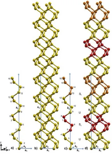
All the strained bulk-silicon structures studied were obtained using the supercell method starting from a unit cell of 16 silicon atoms initially in their bulk centro-symmetric positions. We report in Fig. 1a the unit cell together with the corresponding lattice vectors a1, a2 and a3. The unit cell
is translationally repeated in the whole space by applying the vector R = n1a1 + n2a2+ n3a3
which is a linear combination through the integers n1, n2 and n3 of the lattice vectors. In Fig.
1b we show the repeated unit cell with a couple of cells for each direction.
Figure 1. Unit cells of unstrained and strained bulk-Si structures
Fig. 1(a) Unit cell of 16 Si atoms for unstrained bulk and lattice vectors a1, a2 and a3. Atoms are
labeled with a number from 1 to 16.
Fig. 1(b) Repeated unit cells (2 cells for each direction) as obtained from the application of lattice vectors a1, a2 and a3.
Fig. 1(c) Unit cell of 16 Si atoms for strained bulk (UStUSc/HY3 in the manuscript) and
lattice vectors ã1, ã 2 and ã3. Atoms are labeled with a number from 1 to 16.
Fig. 1(d) Repeated unit cells (2 cells for each direction) as obtained from the application of
In order to obtain the strained structures, we organized the 16 atoms in 4 groups of 4 atoms and we simulated strain by displacing Si atoms of just 2 of the 4 groups as shown in Fig. 1c. We labeled with U (yellow) the silicon atoms which were kept fixed at their bulk positions, while we labeled with S those silicon atoms which distances were modified in order to simulate a compressive Sc (red) and/or tensile St (orange) strain. In order to simulate continuous strain a
crucial point is to choose the lattice vectors coherently with the applied strain as will be explained in details below. We had to re-define new lattice vectors ã1, ã 2 and ã3 for each of the
strained structures and repeating the cell by the vector = n1ã1 + n2ã2+ n3ã3.
We applied a stress moving silicon atoms on the [110] plane along the (001) and (1,-1,0) directions and we identified two class of systems UStUSt and UScUSt (Fig. 2a and Fig. 3a). For
each classes UScUSt and UStUSt we studied three structures in which we have progressively
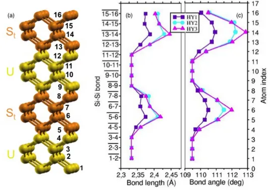
increased the applied strain. In Fig. 2b/c and Fig. 3b/c we show the maximum structural distortion in term of bond lengths and angles for UStUSt and UScUSt structures. The type and magnitude of
strain is qualitatively observed as bond lengths and angles deviations with respect to the unstrained silicon bulk values.
To quantify the stress, each of the six structures have also been characterized by the stress tensor σi=X,Y,Z,j=X,Y,Z and the pressure (HY) [1,2]. In fact, if we consider a volume element (unit cell) of
our stressed structures, we can distinguish the effects of two types of forces: those acting directly in the interior of the element and those exerted upon the surface of the element by the surrounding material. The latter forces are related to the shear stress (SS) which corresponds to the off-diagonal elements of the stress tensor. In Tab. 1 and Tab. 2 we give the values of pressure (HY) and of the yz component of the SS (i.e. σYZ) for the UStUSt and UScUSt structures.
UStUSt HY (GPa) SS (GPa)
HY1 1.71 1.35x10⁻²
HY2 3.06 6.71x10⁻²
HY3 3.06 1.00x10⁻¹
Table 1. Values of pressure (HY) and of the yz component of the SS (i.e. σYZ) for the UStUSt
structures.
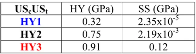
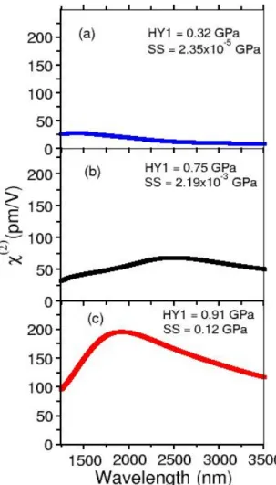
UScUSt HY (GPa) SS (GPa) HY1 0.32 2.35x10⁻⁵
HY2 0.75 2.19x10⁻³
HY3 0.91 0.12
Table 2. Values of pressure (HY) and of the yz component of the SS (i.e. σYZ) for the UScUSt
structures.
We note that the magnitude of pressure and stress is always higher in UStUSt structures than in
UScUSt ones. In fact, as the stress tensor is evaluated per unit-cell volume and it gives
information about the global structure, in the case of UScUSt, the compensation between tensile
and compressive strain (different sign) result in lower HY and SS values. As a consequence the HY and σYZ are meaningful to compare structures only within the same class (i.e. UStUSt or
UScUSt).
R
SUPPLEMENTARY INFORMATION
Figure 2. UStUSt structures.
Fig. 2(a) Simulation unit cell for UStUSt structures. Orange: bonds were elongated to represent a
tensile stress. Yellow: no bond variations with respect to the relaxed silicon lattice (unperturbed region).
Fig. 2(b) Maximum bond length distortions for UStUSt structures. The unstrained bulk-Si bond
lengths are 2.332 Å.
Fig. 2(c) Maximum bond angle distortions for UStUSt structures. The unstrained bulk-Si angles
are 109.5°.
Fig. 3(a) Simulation unit cell for UScUSt structures. Orange: bonds were elongated to represent a
tensile stress. Red: bonds were shortened to represent a compressive stress. Yellow: no bond variations with respect to the relaxed silicon lattice (unperturbed region).
Fig. 3(b) Maximum bond length distortions for UScUSt structures. The unstrained bulk-Si bond
lengths are 2.333 Å.
Fig. 3(c) Maximum bond angle distortions for UScUSt structures. The unstrained bulk-Si angles
are 109.5°.
Lattice vectors for the strained structures:
With our models we simulate continuous strain in a bulk system. A crucial point in the modeling of our structures is the way we have chosen the lattice vectors ã1, ã2 and ã3. In fact, for each
structure these vectors have to be properly and coherently chosen taking into account the applied strain as explained below.
We have chosen ã1=(ã1,0,0) equal to the lattice vector used for the unstrained bulk (a1=(a1,0,0))
as no strain was applied in this direction. Also the vector ã2=(0,ã2,0) is unchanged with respect to
the bulk (a2=(0,a2,0)). In fact, as our unit cell is a chain of atoms the use of vector ã2= a2 permits
to periodically repeat in the Y direction the U (unstrained) regions without introducing any strain and also preserves the system from having strong additional strain at the Sc/St (strained) regions.
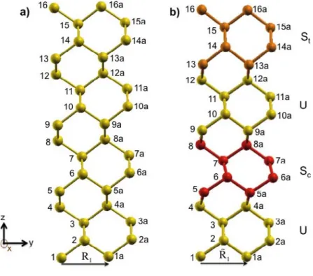
In Fig. 4a/b we show the unstrained and strained silicon unit cell and their replica in Y direction through the vector = 0ã1 +1ã2 + 0ã3 = (0, ã2 ,0). The unstrained silicon unit cell is trivially
repeated (Fig. 4a). For the strained unit cell (Fig. 4b) the U regions still continue to represent an unstrained bulk Si while in the repetition of Sc/St the order of magnitude of strain at the border is
the same as the one in the unit cell itself.
In particular, for UScUSt/HY3 the strain ranges from 0.5% up to 5% while for all the other
structures it ranges from 0.5% up to 3% compared to the bulk Si.
Instead, we modified ã3=(0,0, ã3) with respect to the unstrained bulk value. In fact, our unit cell is
composed in the Z direction, of a compressive Sc and a tensile St regions which globally induce a
change in the height of the cell along this direction. In the definition of ã3 we take into account
this height variation.
Moreover, we also impose a continuity condition between the replica which is explained through Fig. 5a/b. In this figure, we show the unstrained and strained silicon unit cell and its replica in Z direction through the vector = 0ã1 +0ã2 + 1ã3 = (0, 0, ã3).
The continuity condition is to impose that the distance between atom 16 and 1b of the repeated structure is 2.332 Å (unstrained bulk distance). We find that, with respect to the angle of 109.5° in unstrained bulk silicon, these angles differ by ~1%-2% in this connecting region. With this criteria we did not add any strain defects at the edge of the cell between St and U.
R1
R2
SUPPLEMENTARY INFORMATION
Figure 4. Unstrained and strained unit cell repetition in Y direction.
Fig. 4(a) Unit cell for unstrained bulk Si (1-16) and its repetition (1a-16a) through the vector R1 =
0a1 + 1a2+ 0a3= (0, a2 ,0).
Fig. 4(b) Unit cell for strained bulk Si (1-16) and its repetition (1a-16a) through the vector = 0ã1 +1ã2 + 0ã3 = (0, ã2 ,0). The strained structure corresponds to UScUSt/HY3.
Yellow balls/sticks represents the unstrained silicon region, red balls/stick represents the compressive strained region and orangeballs/sticks represents the tensile strain region
R1
Figure 5. Unstrained and strained unit cell repetition in Z direction.
Fig. 5(a) Unit cell for unstrained bulk Si (1-16) and its repetition (1b-16b) through the vector R2
= 0a1 + 0a2+ 1a3= (0, 0, a3).
Fig. 5(b) Unit cell for strained bulk Si (1-16) and its repetition (1b-16b) through the vector = 0ã1 +0ã2 + 1ã3 = (0, 0, ã3). The strained structure corresponds to UScUSt/HY3.
Yellow balls/sticks represents the unstrained silicon region, red balls/stick represents the compressive strained region and orangeballs/sticks represents the tensile strain region.
Below, we give the lattice vectors of all the structures presented:
Unstrained Bulk: |ã1| = 3.808 Å, |ã2| = 3.808 Å, |ã3| = 21.544 Å. UStUSc/HY1: |ã1|= 3.808 Å, |ã2| = 3.808 Å, |ã3| = 21.561 Å. UStUSc/HY2: |ã1| = 3.808 Å, |ã2| = 3.808 Å, |ã3| = 21.726 Å. UStUSc/HY3: |ã1| = 3.808 Å, |ã2| = 3.808 Å, |ã3| = 21.726 Å. UStUSt/HY1: |ã1| = 3.808 Å, |ã2| = 3.808 Å, |ã3| = 21.896 Å. UStUSt/HY2: |ã1| = 3.808 Å, |ã2| = 3.808 Å, |ã3| = 22.271 Å. UStUSt/HY3: |ã1| = 3.808 Å, |ã2| = 3.808 Å, |ã3| = 22.271 Å R2
SUPPLEMENTARY INFORMATION
DOI: 10.1038/NMAT32002) Calculation of
χ
(2)We calculated the ground-state and electronic properties of strained bulk-silicon structures with the Density-Functional Theory (DFT). We used the local-density approximation (LDA), applying norm-conserving pseudopotentials [3] and plane-wave basis set with the ABINIT code [4]. In order to preserve the strain condition we did not relax our models. In fact, we verified that relaxing the systems brought them back into the initial unstrained ones.
We computed the second-order susceptibility
χ
(2) and calculated the second-harmonicgeneration spectra for all the six strained bulk silicon structures. We obtained the nonlinear optical response using the ab initio formalism based on the Time-Dependent Density-Functional Theory (TDDFT) presented in Refs. [5] which has been implemented in the 2light code [6,7]. χ(2) was calculated in the Independent Particle Approximation and a scissor operator of 0.6 eV
was used to simulate the quasiparticle energies [8]. The χ(2) was obtained for light propagating in
the direction (-1,1,0).
In Fig. 6(a/b/c) and Fig. 7(a/b/c) we show second-harmonic generation spectra for the structures
UStUSt and UScUSt respectively. The general trend is that the magnitude of χ(2) increases with
the strain. Moreover, for an equal stress χ(2) is higher in US
cUSt than in UStUSt: actually the
UScUSt present stronger local inhomogeneity due to the change in the sign of the stress between
the Sc and St regions. It is therefore possible, controlling the applied stress, to tune χ(2) intensities
in a very large range, from very few pm/V up to 200 pm/V.
Fig. 6(a)-(c) Calculated χ(2) for SHG spectra for the three structures of Fig. 2(b)-(c). The strain increases from the top to the bottom and manifests a progressive increase in the χ(2) magnitude.
The hierarchy of increasing strain in the three structures (violet-cyan-magenta) is reflected in the corresponding values of pressure (HY) and in the yz component of the Shear Stress (SS).
Figure 7. Simulated χ(2) for SHG spectroscopy in US
cUSt structures.
Fig. 7(a)-(c) Calculated χ(2) for SHG spectra for the three structures of Fig. 3(b)-(c). The strain
increases from the top to the bottom and manifests a progressive increase of the χ(2) magnitude.
The hierarchy of increasing strain in the three structures (blue-black-red) is reflected in the corresponding values of pressure (HY) and in the yz component of the Shear Stress (SS).
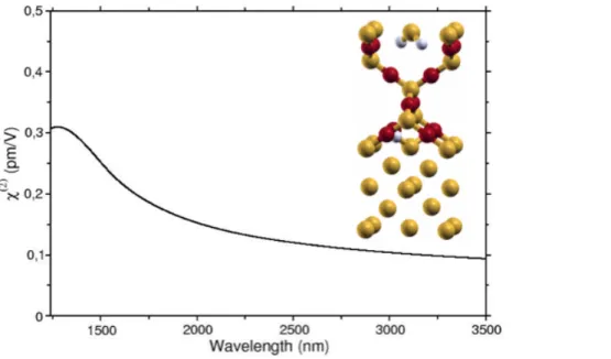
Interface effect on
χ
(2): the example of Si/SiO 2We investigated the role played by interface region supposing unstrained silicon. In fact, with the help of a model system we can neglect the rearrangement of silicon atoms at the interface with another material due to the mismatch between their lattice parameters. Therefore, we calculated the pure interface contribution to χ(2). We considered SiO
2 in thebeta-cristobalite metastable
phase as the interface material (see the inset of Fig.8). This phase of the silicon dioxide has a 6% mismatch in the lattice parameter with respect to Si obtained by growing the SiO2 layer rotated of
45° with respect to Si [9,10]. At the interface a Si atom per unit cell has two dangling bonds, which we saturated by two hydrogen atoms (inset of Fig. 8) [9]. The SiO2 is strongly stressed by
the Si lattice parameter, while Si does not undergo any strain. In Fig. 3) we show the calculated
SUPPLEMENTARY INFORMATION
second-harmonic generation spectrum for the Si/SiO2 interface. Despite the huge stress, the χ(2)
signal is always below 0.5 pm/V in the region of interest. The spectrum is of the order of magnitude of the χ(2) for bulk silicon strained only along (0,0,1). Instead, it is negligible (less then
1%) with respect to the magnitude obtained for strained UScUSt structures where silicon atoms
were moved in the [110] plane (Fig. 7). As a consequence the bulk contribution is expected to be dominant with respect to the interface contribution.
Figure 8. Calculated χ(2) spectrum of the Si/SiO
2 interface.
In the inset the simulation unit cell: Si atoms (yellow balls), O atoms (red balls) and H atoms (white balls).
References
[1] Nielsen, O. H. & Martin, R. M. Quantum-mechanical theory of stress and force. Phys. Rev. B 32, 3780 (1985)
[2] Nielsen, O. H. & Martin, R. M. Stresses in semiconductors: Ab initio calculations on Si, Ge, and GaAs. Phys. Rev. B 32, 3792 (1985)
[3] Luppi, E., et al Accuracy of the pseudopotential approximation in ab initio theoretical spectroscopies. Phys. Rev. B 78, 245124 (2008).
[4] Gonze, X. et al. ABINIT: First-principles approach to material and nanosystem properties.
Computer Phys. Commun. 180, 2582 (2009); Gonze, X. et al. A brief introduction to the ABINIT
software package. Zeit. Kristallogr. 220, 558 (2005).
[5] Luppi, E., Hübener, H. & Véniard, V. Ab-initio second-order nonlinear optics in solids. J. Chem. Phys. 132, 241104 (2010).
[6] Luppi, E., Hübener, H. & Véniard, V. Ab-initio second-order nonlinear optics in solids: Second-harmonic generation spectroscopy from time-dependent density-functional theory.
Phys. Rev. B 82, 235201 (2010).
[7] Hübener, H., Luppi, E. & Véniard, V. Ab initio calculation of many-body effects on the second-harmonic generation spectra of hexagonal SiC polytypes. Phys. Rev. B 83, 115205 (2011).
[8] Godby, R. W., Schluter, M. & Sham L. J. Self-energy operators and exchange-correlation potentials in semiconductors. Phys. Rev. B 37, 10159 (1988).
[9] Seino, K., Wagner, J.-M. & Bechstedt F. Ab initio calculation of optical absorption and