Features
• Single Supply Operation: 2V to 36V • Dual Supply Operation: ± 1V to ±18V
• Allow Comparison of Voltages Near Ground Potential • Low Current Drain 800µA Typ.
• Compatible with all Forms of Logic • Low Input Bias Current 25nA Typ. • Low Input Offset Current ±5nA Typ. • Low Offset Voltage ±1mV Typ.
Description
The LM2903/LM2903I, LM393/LM393A, LM293/ LM293A consist of two independent voltage comparators designed to operate from a single power supply over a wide voltage range.
8-DIP
8-SOP
1
1
Internal Block Diagram
LM2903/LM2903I,LM393/LM393A,
LM293/LM293A
Schematic Diagram
Absolute Maximum Ratings
Parameter Symbol Value Unit
Power Supply Voltage VCC ±18 or 36 V
Differential Input Voltage VI(DIFF) 36 V
Input Voltage VI - 0.3 to +36 V
Output Short Circuit to GND - Continuous
-Power Dissipation, Ta = 25°C 8-DIP 8-SOP PD 1040 480 mW Operating Temperature LM393/LM393A LM2903 LM2903I LM293/LM293A TOPR 0 ~ +70 - 40 ~ +85 -40 ~ +105 -25 ~ +85 °C Storage Temperature TSTG - 65 ~ +150 °C
Electrical Characteristics
(VCC = 5V, TA = 25°C, unless otherwise specified)
NOTE 1
LM393/LM393A: 0 ≤ TA ≤ +70°C
LM2903: -40 ≤ TA ≤ +85°C
LM2903I: -40 ≤ TA ≤ +105°C
LM293/LM293A : -25 ≤ TA ≤ +85°C
Parameter Symbol Conditions LM293A/LM393A LM293/LM393 Unit
Min. Typ. Max. Min. Typ. Max. Input Offset Voltage VIO VO(P) =1.4V, RS = 0Ω - ±1 ±2 - ±1 ±5 mV VCM= 0 to1.5V Note 1 - - ±4.0 - - ±9.0 Input Offset Current IIO - ±5 ±50 - ±5 ±50 nA Note 1 - - ±150 - - ±150 Input Bias Current IBIAS - 65 250 - 65 250 nA Note 1 - - 400 - - 400 Input Common Mode Voltage Range VI(R) 0 -VCC -1.5 0 -VCC -1.5 V Note 1 0 - VCC-2 0 - VCC-2
Supply Current ICC RL = ∞ , VCC = 5V - 0.6 1 - 0.6 1 mA
RL = ∞, VCC = 30V - 0.8 2.5 - 0.8 2.5
Voltage Gain GV VCC =15V, RL ≥ 15KΩ
(for large VO(P-P)swing) 50 200 - 50 200 - V/mV
Large Signal Response Time TLRES VI =TTL Logic Swing VREF =1.4V, VRL = 5V, RL = 5.1KΩ - 350 - - 350 - nS Response Time TRES VRL =5V, RL =5.1KΩ - 1.4 - - 1.4 - µS Output Sink Current ISINK VI(-) ≥ 1V, VI(+) =0V, VO(P) ≤1.5V 6 18 - 6 18 - mA Output Saturation Voltage VSAT VI(-) ≥ 1V, VI(+) = 0V - 160 400 - 160 400 mV
ISINK = 4mA Note 1 - - 700 - - 700
Output Leakage Current IO(LKG) VI(-) = 0V, VI(+) = 1V VO(P) = 5V - 0.1 - - 0.1 - nA VO(P) = 30V - - 1.0 - - 1.0 µA
Electrical Characteristics
(Continued) (VCC = 5V, TA = 25°C, unless otherwise specified)Note 1
LM393/LM393A: 0 ≤ TA ≤ +70°C
LM2903: -40 ≤ TA ≤ +85°C
LM2903I: -40 ≤ TA ≤ +105°C
LM293/LM293A : -25 ≤ TA ≤ +85°C
Parameter Symbol Conditions LM2903/LM2903I Unit
Min. Typ. Max. Input Offset Voltage VIO
VO(P) =1.4V, RS = 0Ω - ±1 ±7
mV
VCM= 0 to 1.5V Note 1 - ±9 ±15
Input Offset Current IIO
- ±5 ±50
nA
Note 1 - ±50 ±200
Input Bias Current IBIAS - 65 250 nA
Note 1 - - 500
Input Common Mode
Voltage Range VI(R)
0 - VCC
-1.5 V
Note 1 0 - VCC-2
Supply Current ICC RL = ∞, VCC = 5V - 0.6 1 mA
RL = ∞, VCC = 30V - 1 2.5
Voltage Gain GV VCC =15V, RL≥15KΩ
(for large VO(P-P)swing) 25 100 - V/mV
Large Signal Response Time TLRES VI =TTL Logic Swing
VREF =1.4V, VRL = 5V, RL = 5.1KΩ - 350 - nS
Response Time TRES VRL = 5V, RL = 5.1KΩ - 1.5 - µS
Output Sink Current ISINK VI(-) ≥ 1V, VI(+) = 0V, VO(P) ≤ 1.5V 6 16 - mA
Output Saturation Voltage VSAT VI(-) ≥ 1V, VI(+) = 0V - 160 400 mV
ISINK = 4mA Note 1 - - 700
Output Leakage Current IO(LKG)
VI(-) = 0V, VO(P) = 5V - 0.1 - nA
Typical Performance Characteristics
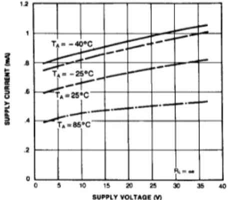
Figure 1. Supply Current vs Supply Voltage Figure 2. Input Current vs Supply Voltage
Figure 3. Output Saturation Voltage vs Sink Current Figure 4. Response Time for Various Input Overdrive-Negative Transition
Figure 5. Response Time for Various Input Overdrive-Positive Transition
Mechanical Dimensions
Package Dimensions in millimeters 6.40 ±0.20 3.30 ±0.30 0.130 ±0.012 3.40 ±0.20 0.134 ±0.008 #1 #4 #5 #8 0.252 ±0.008 9.20 ± 0.20 0.79 2.54 0.100 0.031 () 0.46 ± 0.10 0.018 ± 0.004 0.060 ± 0.004 1.524 ± 0.10 0.362 ± 0.008 9.60 0.378 MAX 5.08 0.200 0.33 0.013 7.62 0.300 MAX MIN 0.25+0.10–0.05 +0.0048-DIP
Mechanical Dimensions
(Continued) Package Dimensions in millimeters 4.92 ± 0.20 0.194 ± 0.008 0.41 ± 0.10 0.016 ± 0.004 1.27 0.050 5.72 0.225 1.55 ±0.20 0.061 ±0.008 0.1~0.25 0.004~0.001 6.00 ±0.30 0.236 ±0.012 3.95 ±0.20 0.156 ±0.008 0.50 ±0.20 0.020 ±0.008 5.13 0.202 MAX #1 #4 #5 0~8 ° #8 0.56 0.022 () 1.80 0.071 MAX0.10 MAX0.004 MAX MIN + 0.10 -0.05 0.15 + 0.004 -0.002 0.0068-SOP
DISCLAIMER
FAIRCHILD SEMICONDUCTOR RESERVES THE RIGHT TO MAKE CHANGES WITHOUT FURTHER NOTICE TO ANY PRODUCTS HEREIN TO IMPROVE RELIABILITY, FUNCTION OR DESIGN. FAIRCHILD DOES NOT ASSUME ANY LIABILITY ARISING OUT OF THE APPLICATION OR USE OF ANY PRODUCT OR CIRCUIT DESCRIBED HEREIN; NEITHER
Ordering Information
Product Number Package Operating Temperature
LM393N 8-DIP 0 ~ + 70°C LM393AN LM393M 8-SOP LM393AM LM2903N 8-DIP -40 ~ + 85°C LM2903M 8-SOP LM2903IN 8-DIP -40 ~ + 105°C LM2903IM 8-SOP LM293N 8-DIP -25 ~ + 85°C LM293AN LM293M 8-SOP LM293AM