proofs JINST_035P_0912
PUBLISHED BYIOP PUBLISHING FORSISSAMEDIALABRECEIVED: September 13, 2012 ACCEPTED: January 11, 2013 PUBLISHED: ???, 2013
14th INTERNATIONAL WORKSHOP ONRADIATION IMAGING DETECTORS,
1–5 JULY 2012,
FIGUEIRA DA FOZ, PORTUGAL
Dedicated multichannel readout ASIC coupled with
single crystal diamond for dosimeter application
A. Fabbri,a,1 M.D. Falco,bF. De Notaristefani,a M. Galasso,aM. Marinelli,c
V. Orsolini Cencelli,aL. Tortora,cC. Veronac and G. Verona Rinatic aDipartimento di Fisica, Universit`a Roma3,
Via della Vasca Navale 84, 00146 Roma, Italy
bDepartment of Diagnostic Imaging, Molecular Imaging, Interventional Radiology and Radiotherapy, Policlinico “Tor Vergata”,
Viale Oxford 81, 00133 Roma, Italy
cDipartimento di Ingegneria Industriale, Universit`a di Roma “Tor Vergata”, Via del Politecnico 1, 00133 Roma, Italy
E-mail:[email protected]
ABSTRACT: This paper reports on the tests of a low-noise, multi-channel readout integrated circuit
used as a readout electronic front-end for a diamond multi-pixel dosimeter. The system is developed for dose distribution measurement in radiotherapy applications.
The first 10-channel prototype chip was designed and fabricated in a 0.18 um CMOS process. Every channel includes a charge integrator with a 10 pF capacitor and a double slope A/D converter. The diamond multi-pixel detector, based on CVD synthetic single crystal diamond Schottky diodes, is made by a 3×3 sensor matrix. The overall device has been tested under irradiation with 6 MeV radio therapeutic photon beams at the Policlinico “Tor Vergata” (PTV) hospital.
Measurements show a 20 fA RMS leakage current from the front-end input stage and a negligi-ble dark current from the diamond detector, a stanegligi-ble temporal response and a good linear behaviour as a function of both dose and dose rate. These characteristics were common to each tested channel.
KEYWORDS: Materials for solid-state detectors; Front-end electronics for detector readout;
Ana-logue electronic circuits; Pixelated detectors and associated VLSI electronics
proofs JINST_035P_0912
Contents
1 Introduction 1
2 Material and methods 2
2.1 Dedicated ASIC design 2
2.2 Diamond multi-pixel dosimeter 2
2.3 Experimental setup 3
3 Results and discussion 3
3.1 Preliminary measurements 3
3.2 Dosimetric characterization 4
4 Conclusions and future work 5
1 Introduction
The introduction of advanced radiation therapy techniques involving the superimposition of narrow high gradient photon beams has produced an increasing interest in high resolution dosimetry. The development of high resolution small volume detectors was studied by several authors with the aim of designing new devices for accurate dosimetry in high energy narrow photon beams [1–3]. In this field, diamond has long been considered a suitable material for the construction of small volume radiation detectors due to its radiation hardness, near tissue-equivalence, small size, high sensitivity and low leakage current [4–6]. The development of Schottky diode diamond detectors were recently realized and tested as radiotherapy dosimeters with different beam types for clinical dosimetry [7,8]. Since the beams are generally characterized by strong spatial gradients, the use of diamond dosimeters with good spatial resolution is necessary in order to have a good mapping of the radiotherapy beam. In order to measure these high field gradients, the use of a dosimeter matrix is a possible solution even if the increase in the number of sensitive elements requires a cor-responding increase in the number of readout channels. The current signal measurement is usually done with an electrometer connected to the sensor with a triaxial cable. This measurement setup, due to the size of the connections and to the size and cost of the measurement devices, is hardly usable with more than a single device at the same time. Using an integrated multi-channel readout chip closed to the detector solves this problem, furthermore it allows reducing to the minimum the overall sensor size. Moreover the application-specific integrated circuit, (ASIC) can also perform the D/A conversion, reducing to the minimum the wires going to the measurement field.
In this work, a dedicated multichannel readout ASIC, coupled with a multi-pixel single crystal diamond Schottky diode dosimeter, has been developed and tested under irradiation with high energy radiotherapeutic photon beams.
proofs JINST_035P_0912
Figure 1. Channel frontend schematic: due to the very low input impedance to Vref of the input stage, thediamond sensors works with roughly 0 V polarization, as emphasized in the right simplified schematic.
2 Material and methods
2.1 Dedicated ASIC design
The ASIC, developed at Roma3 University, is composed of a 10-channel readout system with a digital serial output A/D converter dedicated to each channel. The acquisition channel block dia-gram is presented in figure1. The diagram shows that the channel was designed with an interleaved architecture: while one channel is making the A/D conversion the other is kept in acquisition in order to reduce the acquisition dead time to zero. This solution was adopted to avoid dose mea-surement loss during the conversion phase of the ADC. The A/D conversion is performed using a single ramp converter. After the conversion the digital data from all the channels are packed in a serial register and transferred serially to the remote PC through a control board based on an FPGA. The FPGA also sets the integration time, the clock frequency and other digital switches used during the test and calibration phase. The standard acquisition time is 50 ms, as the current expected from a single dosimeter is in the range of 5–100 pA corresponding to a voltage slope on the integration capacitor of 25–500 mV.
2.2 Diamond multi-pixel dosimeter
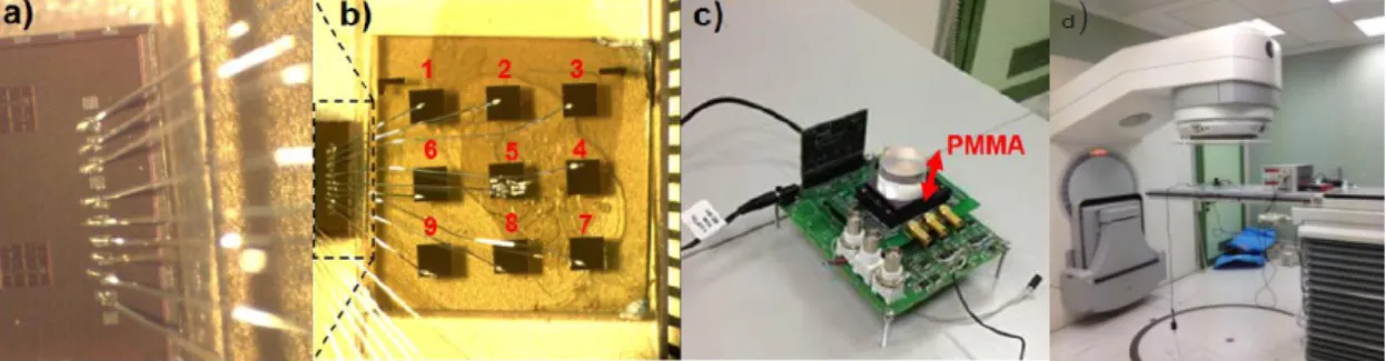
The dosimeter, fabricated at “Tor Vergata” University, is based on a combination of chemical va-por deposition (CVD) intrinsic and boron-doped single crystal diamond (SCD) films homoepitax-ially grown on high temperature high pressure (HPHT) commercial <100> Ib diamond substrate, 4×4×0.5 mm2 in size. At first, a highly conductive boron-doped SCD film is deposited upon the HPHT substrate, then an extremely pure SCD intrinsic layer is grown on the p-type diamond. Fi-nally, standard photolithographic techniques and thermal evaporation are used for patterning the surface of intrinsic CVD diamond film with an array of rectifying Schottky Al pads. A 3×3 ar-ray, which consists of 500 µm Al squares at a distance of 500 µm, was realized (figure2(b)). The resulting sensitive area is approximately 0.25 mm2 for each pixel. As clearly seen in figure2(a), all pixels of the array were micro-soldered to the readout ASIC. The coplanar array of Schottky electrodes defines the pixel sequence of the dosimeter and the boron doped SCD acts as a grounded
proofs JINST_035P_0912
Figure 2. CVD-ASIC assembly photography a) readout ASIC, b) sensor matrix, c) reading circuit boardand PMMA tissue equivalent phantom and d) experimental setup at PTV hospital.
common buffer layer. This device operates in a sandwich geometry in order to exploit the internal junction electric field [9]. In this way, each electrode of the diamond dosimeter can be operated at 0 V bias obtaining a very low dark current.
2.3 Experimental setup
The measurements were performed at the Policlinico “Tor Vergata” (PTV) hospital. Dosimetric measurement were carried out with 6 MeV photons generated by an Elekta Precise Linear Acceler-ator (LINAC) as shown in figure2(d). The diamond dosimeter was assembled on the reading circuit board and a phantom made on PMMA (Poly Methyl Meta Acrylate) cylinder (about 2 cm high) was placed in front of the detector during the irradiation (see figure2(c)). On the right side of the fig-ure2(d), out of the radio treatment field, it is possible to see the power supplies. The bulky bench devices will be soon substituted by dedicated circuitry exploiting the USB interface standard power supply. At present time the hp/matrix assembly is mounted on a very large test board. This is nec-essary to operate the many test circuitries that are present on this version of the chip. These are used to check the internal behavior of the device and verify that it is working according to its specifica-tions. These auxiliary circuitries are not needed in the normal operating condition and their control wiring will not be connected, reducing the overall device outline to a few millimeters side rectangle.
3 Results and discussion
3.1 Preliminary measurements
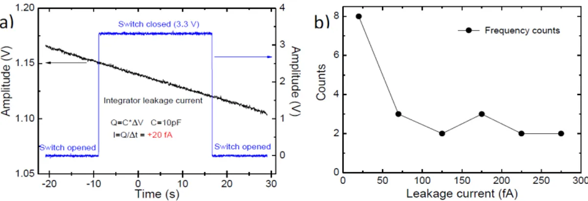
A first test was made to characterize the diamond sensor and front-end leakage current and dark current. Figure3(a) shows the charge integrator output voltage plot during an interval of 50 sec-onds. The switch connecting the front-end to the diamond dosimeter was first opened and then closed. In both conditions, there is no appreciable variation in the slope of the signal, indicating that the dark current of the diamond dosimeter is very close to zero and is not measurable in these conditions. By the slope value, knowing the integrating capacitance (10 pF), it is possible to calcu-late the integrated leakage current. In the best condition, a value of about 20 fA has been measured. The frontend (2 for each channel) leakage current distribution is shown in figure3(b). These values depend from the typical IC fabrication process spread and, in the worst case, are less than 300 fA, that is the current limit that can be evaluated.
proofs JINST_035P_0912
Figure 3. a) Leakage current measurement (black line) by opening and closing the switch connecting thefrontend to the diamond dosimeter (blue line); b) leakage current distribution.
Figure 4. a) Time response and b) 3D amplitude map of the nine pixels at 6 MeV.
In order to calculate the input gain factor for each channel, a constant current was applied to the readout channel inputs. In our case, the gain factor depends on the value of the current supplied by the mirror used to discharge the integrator capacitance from the stored charge. In fact the input gain spread can be as high as 23%. This depends on the low value used for the discharge current (few pA) because it was non convenient to polarize the mirror devices with a strong overdrive due to die space limitations.
3.2 Dosimetric characterization
The diamond dosimeter, connected with the multichannel readout ASIC, was placed inside the square shaped radiation field, 3×3 cm2in size. Temporal response and related 3D amplitude map of the nine pixels under irradiation of 6 MeV photon energy are shown in figure4. Despite the high radiation flux neitherelectronic noisenorsignalinstability is found during data acquisition, demon-strating the ASIC’s radiation hardness. All nine channels show similar behavior in terms of time response and the measured signal to dark ratio is greater than 1000. The typical currents measured are tens of pA with a noise of about 2%. The responses are reproducible and no undesired effects such as persistent photocurrent or memory effects are observed. However, the sensitivity of the nine pixels show a variation of about 23%, as expected from the gain calibration as reported above.
proofs JINST_035P_0912
Figure 5. a) Response vs. dose and b) dose rate for 6 MeV photon energy. Full lines are law function bestfits.
The dose dependence of the nine pixel response was studied at a fixed dose rate of about 3 Gy min−1 in delivered doses up to 5 Gy. The results are shown in figure 5(a) under irradiation of 6 MeV photon energy. In all cases a good linear behavior was observed and the linearity index ∆ for different pixels was found to be in the range 0.991÷1.013, as given by fitting experimental data with the law function y=a·x∆. The a for the nine pixels parameter was found in the rage (2.16÷2.49) ·106Counts/Gy. The dose rate dependence was also investigated in the range from approximately 0.5 to 5 Gy min−1. In particular, the dose rate was varied by changing the pulse repetition frequency of the accelerator. In figure 5(b) is reported the average current (counts/s) during irradiation as a function of the dose rate. The values of ∆ for the nine channels was found in the range 0.951÷1.005 indicating a very low dose rate dependence. The a parameters obtained for the nine pixels are in the (2.13÷2.38)·106Counts/Gy range. In particular, all the values of the a parameter are compatible within 5% with the ones determined by the dose linearity curves.
4 Conclusions and future work
A multichannel readout ASIC coupled with a multi-pixel synthetic single crystal diamond dosime-ter has been successfully developed in a collaboration by “Roma 3” and “Tor Vergata” Universities and characterized at the PTV hospital under irradiation of 6 MeV photon energy.
Test results have shown a very low dark current of the diamond dosimeter pixel, negligible compared with the integrator leakage current of about 20 fA. No electronic noise from the readout ASIC and no evidence of memory effect or persistent photocurrent under irradiation doses was observed for each pixel. Finally, dose and dose rate dependence tests have evidenced a good linear behaviour with a linearity index close to 1 for all the nine channels.
Work is in progress to design the diamond dosimeter and the readout ASIC with more chan-nels/pixels in order to improve the spatial resolution of the overall device. Moreover, the diamond-readout ASIC assembly will be enclosed in an epoxy resin (waterproof requirement) for mea-surements in a water phantom. The final device will be about 5 mm × 8 mm, with 5-wire cable connection to a host device for data storage and control.
proofs JINST_035P_0912
Acknowledgments
The work was supported by the Fondazione Roma.
References
[1] M. Westermark, J. Arndt, B. Nilsson and A. Brahme, Comparative dosimetry in narrow high-energy photon beams,Phys. Med. Biol.45 (2000) 685.
[2] A. Appleby and A. Leghrouz, Imaging of radiation dose by visible color development in ferrousagarosexylenol orange gels,Med. Phys.18 (1991) 309.
[3] P. Francescon, S. Cora and C. Cavedon, Total scatter factors of small beams: A multidetector and Monte Carlo study,Med. Phys.35 (2008) 504.
[4] E.A. Burgemeister, Dosimetry with a diamond operating as a resistor,Phys. Med. Biol.26 (1981) 269. [5] S.N. Rustgi and D.M. Frye, Dosimetric characterization of radiosurgical beams with a diamond
detector,Med. Phys. 22 (1995) 2117.
[6] M. Bucciolini et al., Diamond detector versus silicon diode and ion chamber in photon beams of different energy and field size,Med. Phys.30 (2003) 2149.
[7] S. Almaviva et al., Synthetic single crystal diamond dosimeters for Intensity Modulated Radiation Therapy applications,Nucl. Instrum. Meth.A 608 (2009) 191.
[8] I. Ciancaglioni et al., Dosimetric characterization of a synthetic single crystal diamond detector in clinical radiation therapy small photon beams,Med. Phys.39 (2012) 4493.
[9] A. Almaviva et al., Chemical vapor deposition diamond based multilayered radiation detector: Physical analysis of detection properties,J. Appl. Phys.107 (2010) 014511.