© 2011 WILEY-VCH Verlag GmbH & Co. KGaA, Weinheim Phys. Status Solidi RRL 5, No. 2, 80– 82 (2011) / DOI 10.1002/pssr.201004488
www.pss-rapid.com
pss
Lateral IBIC characterization of single
crystal synthetic diamond detectors
Alessandro Lo Giudice1 , Paolo Olivero*, 1 , Claudio Manfredotti1 , Marco Marinelli2 , Enrico Milani2 , Federico Picollo1 , Giuseppe Prestopino2 , Alessandro Re1 , Valentino Rigato3 , Claudio Verona2 , Gianluca Verona-Rinati2
, and Ettore Vittone1
1 Experimental Physics Department – NIS Centre of Excellence, University of Torino and INFN – sez. Torino, via P. Giuria 1, 10125 Torino, Italy
2 Dipartimento di Ingegneria Meccanica, Università di Roma “Tor Vergata”, Via del Politecnico 1, 00133 Roma, Italy 3 INFN- National Laboratories of Legnaro, Viale dell’Università 2, 35020 Legnaro (Pd), Italy
Received 16 November 2010, revised 5 January 2011, accepted 6 January 2011 Published online 11 January 2011
Keywords single crystals, diamond, ion beam induced charge, charge transport, detectors
* Corresponding author: e-mail [email protected], Phone: +39 011 670 7879, Fax: +39 011 669 1104
© 2011 WILEY-VCH Verlag GmbH & Co. KGaA, Weinheim
1 Introduction Diamond has extreme electronic and optical properties. The low intrinsic conductivity due to the wide bandgap, the high carrier mobility, the high thermal conductivity, the chemical inertness and the radiation hard-ness make it a good candidate as particle, UV and X-ray detector in many fields, especially in high radiation environments [1–4]. Although good results were obtained in the past using natural, high pressure high temperature (HPHT) and chemical vapor deposition (CVD) poly-crystalline diamond, the last decade witnessed a vast improvement in the diamond detectors performances due to the development of homoepitaxial diamond (single crystal, SC) growth [5]. This material is characterized by high purity and low defect concentration, it exhibits long charge carrier lifetimes, high mobility and does not require a prim-ing procedure before operation [6–8]. Recent results ob-tained in the detection of UV light [9], X-rays [10] and neu-trons [11] with SC-diamond detectors are very promising.
Ion beam induced charge (IBIC) is a very suitable technique to characterise transport properties in wide band
gap semiconductors employed as ionizing radiation detec-tors [12]. SC-diamond detecdetec-tors were already studied by means of frontal IBIC [13]. In this Letter we report on the characterization of diamond SC Shottky diodes by means of lateral IBIC technique.
2 Experimental The device was developed starting from a single-crystal diamond grown by CVD technique at the laboratories of Rome “Tor Vergata” University. Dia-mond was grown on a HPHT substrate in a p-type/intrinsic layered structure by a two-step plasma-enhanced micro-wave CVD homoepitaxial deposition process. A cross-sec-tional schematic of the device is reported in Fig. 1. A
com-mercial HPHT Ib single crystal diamond 4 × 4 × 0.4 mm3
in size was used as substrate. A ~ 20 μm thick heavily
boron-doped (~1020 cm–3) layer was first deposited on the
HPHT substrate followed by the deposition of a 30 μm thick diamond layer with a net electrically active
acceptor-like defect concentration of the order of 1014 cm–3 [10].
A circular Al contact with a diameter of 2 mm and 200 nm
In order to evaluate the charge collection efficiency (CCE) profile of single-crystal diamond devices based on a p-type/ intrinsic/metal configuration, a lateral Ion Beam Induced Charge (IBIC) analysis was performed over their cleaved cross sections using a 2 MeV proton microbeam. CCE pro-files in the depth direction were extracted from the cross-sectional maps at variable bias voltage. IBIC spectra relevant to the depletion region extending beneath the frontal Schottky
electrode show a 100% CCE, with a spectral resolution of about 1.5%. The dependence of the width of the high effi-ciency region from applied bias voltage allows the constant residual doping concentration of the active region to be eval-uated. The region where the electric field is absent shows an exponentially decreasing CCE profile, from which it is pos-sible to estimate the diffusion length of the minority carriers by means of a drift–diffusion model.
Phys. Status Solidi RRL 5, No. 2 (2011) 81
www.pss-rapid.com © 2011 WILEY-VCH Verlag GmbH & Co. KGaA, Weinheim
Rapid Research Letter
Figure 1 (online colour at: www.pss-rapid.com) Schematics of the diamond detector cross-sectional structure, connection to the acquisition electronic chain, and ion beam probe geometry. The drawing is not to scale.
thick was then deposited on the intrinsic diamond surface, while annealed ohmic silver back electrodes were formed on the heavily B-doped layer (see Fig. 1). The sample was cleaved in order to expose the cross section to the ion beam irradiation and edge-on mounted to perform lateral IBIC experiments.
IBIC measurements were carried out at the AN2000 microbeam facility of the National Laboratories of Legnaro (Italy) by using 2 MeV protons. The beam was focused to a spot size of ~2 μm and raster-scanned over the cleaved cross section of the diamond sample from the Schottky
contact to the highly doped substrate (62 × 62 μm2 scan
area), as schematically shown in Fig. 1.
As evaluated by the SRIM Monte Carlo Simulation code [14], the range of 2 MeV protons in diamond is about 25 μm, while their lateral straggling is ~0.66 μm. Since the electron/hole generation occurs primarily at the Bragg’s peak, it is reasonable to assume negligible charge or re-combination effects at the irradiated cross-section surface. As a consequence, the induced charge signals collected at the sensitive frontal electrode can be considered as due to the motion of free carriers generated in the bulk of the dia-mond sample, and subjected to an electric field oriented orthogonally to the two electrodes.
The system provided a spectral sensitivity of 270 elec-trons/channel and a spectral resolution (defined as the FWHM of the 2 MeV proton peak in the Si surface-barrier detector used as reference) of about 3900 electrons, corre-sponding to an energy resolution of 14 keV in silicon.
3 Results and discussion Room temperature cur-rent–voltage (I–V) characterization in reverse and forward polarizations yielded a good rectification effect due to the presence of a Schottky barrier at the Al electrode, whereas the highly doped back contact is assumed to be ohmic.
The linear behaviour of the I–V curve in reverse po-larization for V < –20 V indicated the presence of a shunt
resistance Rsh = (900 ± 6) GΩ. From the forward bias
be-haviour an ideality factor n = (1.51 ± 0.04), a series
resis-tance Rs = (5.1 ± 1.6) kΩ and a saturation reverse current
of (1.0 ± 0.6) ⋅ 10–23 A were derived. The high value of R
s
Figure 2 (online colour at: www.pss-rapid.com) Lateral IBIC maps relevant to bias voltages: a) 0 V, b) 25 V, c) 60 V. The ver-tical lines at the bottom of the maps indicate the position of the Schottky (S) frontal sensitive electrode and of the B doped back electrode (B).
is probably due to the highly B-doped electrode at the bot-tom of the active region. Assuming an effective
Richard-son constant of 92 A cm–2 K–2 [15], the barrier height can
be estimated around 1.4 eV.
Figure 2 shows lateral IBIC maps at different reverse bias voltages. The CCE is encoded in colour scale, being derived from the median of the IBIC pulse distribution for each pixel. The highest charge is induced by the motion of carriers generated in the proximity of the Schottky elec-trode, which roughly corresponds to the depletion region where a strong electric field occurs. At zero bias, the maxi-mum induced charge occurs in a region extending around 5 μm beneath the Schottky barrier; as the applied bias in-creases, the extension of the high efficiency IBIC region widens.
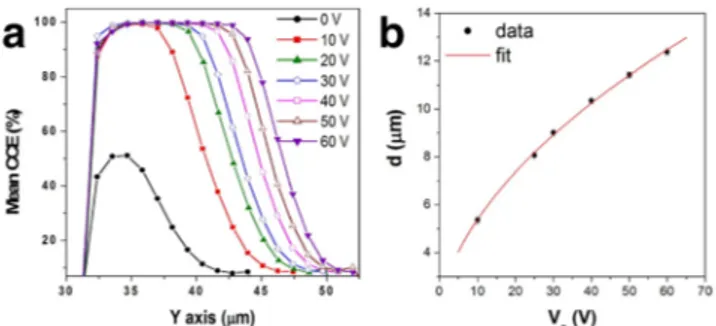
In Fig. 3a the CCE profiles obtained by projecting the CCE maps along the y-axis are reported. These profiles exhibit the same behavior observed in previously analyzed partially depleted silicon p–n junctions [16] and Schottky diodes [17], which have been interpreted using the drift– diffusion model for charge induction based on the Shockley–Ramo–Gunn theorem [12].
In a simplified version of this model, charge pulses are formed only in regions where an electric field (E) is pre-sent, i.e. within the depletion region W, and the amount of the induced charge is proportional to the d/W ratio, where
d = μ ⋅ τ ⋅ E is the carrier drift length and μ ⋅ τ is the
mobil-ity (μ)–lifetime (τ) product. Due to the fast drift, no re-combination occurs during the time of flight of electron and holes throughout the thickness W, and the induced charge is equal to the generation charge (i.e. CCE = 100%) for carriers generated within the depletion region, which widens as the applied bias voltage increases. Moreover, the dependence of the extension of the depletion region W
from the applied voltage Va can be interpolated with the
well known formula:
(
)
r 0 a bi A
2 ( )
82 A. Lo Giudice et al.: Lateral IBIC characterization of SC synthetic diamond detectors
© 2011 WILEY-VCH Verlag GmbH & Co. KGaA, Weinheim www.pss-rapid.com
status solidi
physica
rrl
Figure 3 (online colour at: www.pss-rapid.com) (a) CCE profiles at different bias voltages. (b) Plot of the extension of the deple-tion region as evaluated from the IBIC maps as a funcdeple-tion of ap-plied bias voltage.
where εr and ε0 are the relative and vacuum dielectric
con-stants, e is the elementary electrical charge, NA is the net
electrically active acceptor-like defect concentration and
Vbi is the built-in potential at the Schottky barrier. As
shown in Fig. 3b, the experimental data are satisfactorily fitted by this trend, yielding a value of the built-in voltage of (1.3 ± 0.8) V, to be compared with the value (1.4 V) ob-tained by C–V measurement, and an estimation of the net electrically active acceptor-like defect concentration of
NA = (2.43 ± 0.13) × 1014 cm–3, in good agreement with
previous estimations [10].
On the other hand, for y > W, i.e. in the region where no electric field is present, electrons and holes diffuse away from the generation point. The charge at the sensing electrode is induced only by the motion of free carriers in presence of the applied electric field, so no induction oc-curs from their motion in the neutral region [12]. However, their thermal random motion produces a diffusion current towards the depleted region. While majority carriers (holes) are driven back by the electric field, the minority carriers (electrons) penetrate this region, are drifted to-wards the sensitive electrode, and induce a current pro-portional to their flux. Being diffusion a much slower transport mechanism, recombination effects attenuate the population of electrons entering the active region. As the distance of the generation point from the depletion region increases, assuming an homogeneous material through- out the entire epitaxial layer, the probability of electrons to enter the depletion region exponentially decreases, with a logarithmic slope equal to their diffusion length
Le = (De⋅ τe)1/2, where De and τe are the electron diffusivity
and lifetime, respectively. The fit procedure of the expo-nentially decreasing tails reported in Fig. 3a provides an
average electron diffusion length of Le = (2.6 ± 0.2) μm, in
excellent agreement with the value reported in [10]. Using the Einstein relation for the diffusivity/mobility ratio, the
product of the zero field mobility (μe) and the lifetime is
evaluated as μe⋅ τe = (2.5 ± 0.3) × 10–6 V cm–2, a value
which is in good agreement with what reported in [6, 18],
providing an electron lifetime estimate of ~1 ns, if a
mobil-ity of the order of 2000 cm2 V–1 s–1 is considered [19, 20].
4 Conclusions Lateral IBIC characterization was em-ployed to characterize the charge transport properties of SC diamond devices. In the active region, the device yield-ed a 100% efficiency with a spectral resolution of about 35 keV. The variation of the width of the depletion region as function of the applied bias voltage allows the estima-tion of the acceptor-like defect concentraestima-tion in the
nomi-nally intrinsic layer to a value of (2.43 ± 0.13) × 1014 cm–3.
The analysis of the tails of the CCE profiles provides a value of the mobility–lifetime product for electrons of
2.5 × 10⁻⁶ cm2 V–1, which corresponds to an average
life-time of the order of ~1 ns if typical mobility values are assumed.
Acknowledgements This work was supported in the
framework of the INFN experiment DIARAD and MiUR-PRIN2008 National Project “Synthetic single crystal diamond dosimeters for application in clinical radiotherapy”. The work of P. Olivero was supported by the “Accademia Nazionale dei Lincei – Compagnia di San Paolo” Nanotechnology grant.
References
[1] A. Paoletti and A. Tucciarone (Eds.), The Physics of Dia-mond (OS Press, Amsterdam, 1997).
[2] J. H. Kaneko et al., Nucl. Instrum. Methods Phys. Res. A
505, 187 (2003).
[3] W. Adam et al., Nucl. Instrum. Methods Phys. Res. A 565, 278 (2006).
[4] D. Tromson et al., Diam. Relat. Mater. 19, 1012 (2010). [5] J. Isberg et al., Science 297, 1670 (2002).
[6] J. Isberg et al., Diam. Relat. Mater. 13, 872 (2004). [7] M. Pomorski et al., Diam. Relat. Mater. 16, 1066 (2007). [8] N. Nesladek, Diam. Relat. Mater, 17, 1235 (2008). [9] S. Almaviva et al., Diam. Relat. Mater. 19, 78 (2010). [10] S. Almaviva et al., J. Appl. Phys. 107, 014511 (2010). [11] S. Almaviva et al., Nucl. Instrum. Methods Phys. Res. A
612, 580 (2010).
[12] M. B. H. Breese et al., Nucl. Instrum. Methods Phys. Res. B
264, 345 (2007).
[13] C. Manfredotti et al., Diam. Relat. Mater. 16, 940 (2007). [14] J. F. Ziegler, J. P. Biersack, and M. D. Ziegler, SRIM – The
Stopping and Range of Ions in Matter (Ion Implantation Press, 2008).
[15] R. Kumaresan et al., Diam. Relat. Mater. 19, 1324 (2010). [16] C. Manfredotti et al., Nucl. Instrum. Methods Phys. Res. B
158, 476 (1999).
[17] P. Olivero et al., accepted for publication in Nucl. Instrum. Methods Phys. Res. B (2010).
[18] A. Lohstroh et al., Appl. Phys. Lett. 90, 102111 (2007). [19] L. S. Pan and D. R. Kania, Diamond: Electronic Properties
and Applications (Kluwer Academic Publishers, Boston– Dordrecht–London, 1993).