ARCES – ADVANCED RESEARCH CENTER ON ELECTRONIC SYSTEMS FOR INFMORMATION AND COMMUNICATION TECHNOLOGIES E. DE CASTRO
SCUOLA DI DOTTORATO IN TECNOLOGIE DELL’INFORMAZIONE
CICLO XXV ING-INF/01MODELLING AND DESIGN OF
ADVANCED RELIABLE CIRCUITS AND
DEVICES FOR ENERGY EFFICIENCY
Tesi di Dottorato
Presentata da Daniele Giaffreda
Coordinatore della scuola di Dottorato: Chiar.mo Prof. Ing. CLAUDIO FIEGNA Relatore:
Chiar.ma Prof.ssa Ing. CECILIA METRA Chiar.mo Prof. Ing. CLAUDIO FIEGNA
Contents
_____________________________________________________________________
Chapter 1 14
1.1 Reliability and modelling for electronic systems 14
Chapter 2 22
2.1 Security problems of standard protocols 24
2.2 Proposed secure protocol 24
2.3 Implementation and validation 28
2.4 Summary 31
Chapter 3 34
3.1 Considered Measurement Scheme for Process Parameter Variation 36 3.2 Proposed On-‐Die Measurement Scheme 37
3.3 Measurement Accuracy 43
3.3.1 Cost evaluation and comparison 47
3.4 Summary 48
Chapter 4 53
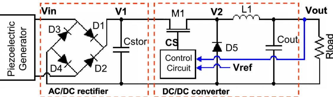
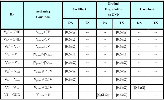
4.1 The self powered wearable multisensor considered 55 4.2 Faults Affecting the Energy Harvesting Circuit and their Effects 57 4.2.1 Faults affecting the AC/DC rectifier and produced effects 58 4.2.2 Faults affecting the DC/DC converter and produced effects 62 4.3 Proposed Energy Harvesting Concurrent Monitoring Circuit 65 4.3.1 Implementation and validation 68
4.4 Self-‐checking ability 70
4.5 Cost evaluation 76
4.6 Summary 78
Chapter 5 83
5.2 Thermal model description and validation 89 5.3 Solar Cell thermal behavior derived from the model 94
5.4 Summary 99
Chapter 6 105
6.1 Description of distributed electrical network 106 6.1.1 Optimum size of the elementary units 108 6.2 Parameters extraction for the calibration of the distributed electrical
model 109
6.2.1 Thermographic characterization of solar cell 111 6.2.2 Dark I-‐V measurement of solar cell 112 6.2.3 Simulation results obtained with the distributed electrical model
calibrated 113
6.4 A case of study: effect of local shunts and its modeling in a silicon solar cell
117
6.5 Summary 125
Conclusion 127
Appendix A 131
A.1 The “real value” of contact resistance in a solar cell 131 A.2 Transmission Line Model applied to measure the contact resistance 133
List of figures
Figure 1.1: Temporal behavior of the clock signal affected by jitter. ... 16 Figure 2.1: Structure of a MAC or ACK of the proposed protocol. ... 25 Figure 2.2: Sequences of the rolling code memorized on a master node (N1) and slave nodes (N2, N3, N4). ... 26 Figure 3.1: Internal structure of the FUBs in [3-10]. ... 36 Figure. 3.2: Block structure of the proposed measurement scheme. ... 37 Figure 3.3: (a) (b) Schematic representation of the propagation of the CK falling and rising edges, respectively, through the RO gates, when the proposed scheme is used to measure jitter. ... 38 Figure 3.4: Possible implementation of blocks MS and OS (a), and block CB (b) [3-9]. ... 40 Figure 3.5: Block structure of the proposed scheme providing higher measurement resolution than that in Fig. 3.1. ... 41 Figure 3.6: Schematic representation of the signals produced at the NOT outputs when the circuit is used to measure CK jitter. ... 42 Figure 3.7: Oscillation periods of the ROs in [3-10] (TRO_[3-10]), and in the
proposed scheme (TRO_our), as a function of parameters Vth (a) and Tox
(b). ... 44 Figure 3.8. Simulation results for nominal values of electrical parameters and case of: i) no jitter (CK HP 1); ii) jitter of 7ps (CK HP 2). ... 45 Figure 4.1: EHC used to power the considered multisensor node. ... 55 Figure 4.2: Variation of the voltage on Vout due to a BF (with RBF = 1kΩ)
Figure 4.3: Variation of the voltage on nodes Vout (solid line) and V1 (dashed
line) in case of a BF (with RBF = 500Ω) between them. ... 61
Figure 4.4: Simulation results showing the variation of the voltage on Vout due
to a BF (with RBF = 500Ω) between Vout and GND. ... 65
Figure 4.5: Proposed monitoring circuit ... 66 Figure 4.6: Simulation results obtained for nominal values of electrical parameters and temporary drop of Vout (due to faults) greater than the 28%
of its nominal value. ... 68 Figure 4.7: Monte Carlo simulations showing the minimum voltage value on Vout resulting in an error indication in case of statistical variations of
electrical parameters up to 20%. ... 69 Figure 4.8: Inverter derived from [4-17] allowing logic threshold calibration after fabrication. ... 70 Figure 4.9: Considered BFs (a), and maximum R value for which they can be detected (b). ... 75 Figure 4.10: (a) Power consumed by the proposed monitoring circuit as a function of its operating frequency. (b) Power consumed by EHC (squares pattern) and by the monitoring circuit (circle pattern), as a function of the frequency fCS of the control signal Vcs. ... 76
Figure 5.1: Two diode equivalent lumped model of a solar cell ... 84 Figure 5.2: Dark and illuminated I-V, power curve, and basic solar cell parameters. ... 85 Figure 5.3: Two diode modified equivalent lumped model of a solar cell [5-2].
... 86 Figure 5.4: Solar cell current IPV as a function of VPV for a PV cell modeled
with the circuit in Fig. 5.3 for the case of an irradiation Girr=500W/m2
producing an IPV=4A and for three different values of the shunt resistance
RSH. ... 87
Figure 5.5: Cross-section of an encapsulated silicon solar cell (glass-EVA-ARC - Silicon-Tedlar) [5-20]. ... 89
Figure 5.6: (a) Proposed equivalent thermal model to estimate the time dependence of the temperature of the portion of PV cell (AHS) under
hot-spot condition. (b) Schematic representation of a shaded PV cell considered here to build the model. ... 91 Figure 5.7: Temperature trend over time in solar cell, when it is fully shaded after t1 and for the operation conditions reported in [5-5]. ... 94 Figure 5.8: Considered PV array scheme used to analyze (by means of the proposed model) the temperature behavior in time of a shaded PV cell (PV36) undergoing a hot-spot condition. ... 95 Figure 5.9: Results obtained with the model for the temperature THS behavior
of PV36 when: (a) PV36 becomes fully shaded after t1a (γ=0.01) and for
various values of RSH; b) PV36 becomes partially shaded after t1b (with
γ=0.3) and with the lowest value of RSH =112Ω (worst case from the cell
temperature point of view). ... 97 Figure 5.10: Results obtained with the thermal model for the temperature behavior of PV36 when: (a) PV36 becomes fully shaded after t1c (γ=0.01)
and for different values of its reverse voltage (Vpv varying from 9.1 to
-9.6V); (b) PV36 becomes partially shaded after t1d (γ=0.3) and with the
lowest of the considered reverse voltages in Fig. 5.10(a) (worst case from the temperature point of view). ... 98 Figure 6.1: Elementary units implemented in the distributed electrical network. They are based on the 2-diode model. The elementary unit (a) is suitable to model the area under the fingers and the busbars. The elementary unit (b) allows modeling the area under non-metalized regions. ... 106 Figure 6.2: Distributed network model of a single junction silicon solar cell. The network describes the complete solar cell including busbars, fingers, illuminated areas as well as the perimeter. ... 108 Figure 6.3: Dark I-V characteristic with two different regions. ... 110 Figure 6.4: (a) Schematic diagram of spatially resolved thermography measurement setup. (b) Synchronous-pulse thermography image of the analyzed cell. ... 112
Figure 6.5: Dark I-V characteristic measured of the mc-Si solar cell. ... 113 Figure 6.6: Comparison between experimental and simulated dark I-V curves.
... 114 Figure 6.7: Experimental and simulated I-V curves under different illumination levels. ... 115 Figure 6.8: (a) 2-D Voltage distribution across the whole solar cell when a forward bias around the maximum power point is applied and under a power irradiation of 1000W/m2. (b) Zoom in (not in scale) of the 2-D voltage distribution in a local region of the solar cell. ... 116 Figure 6.9: Synchronous-pulse thermography image of the analyzed shunted cell. ... 117 Figure 6.10: Comparison between experimental and simulated dark I-V curves for a shunted solar cell. ... 118 Figure 6.10: Experimental and simulated I-V curves under different illumination levels of the shunted solar cell. ... 119 Figure 6.11: Schematic representation of the solar cell with the simulated
hot-spot area. The highlighted shunt resistances in the distributed model represent the local region with a very low value of the resistance respect the remained solar cell. ... 120 Figure 6.12: Experimental and simulated I-V curves obtained by considering different values of local specific shunt resistance in the hot-spot area (1.6 cm2) under 1.18 Sun. ... 121 Figure 6.12: 2-D Voltage distribution across the whole solar cell with a low shunt resistance when a forward bias around the maximum power point is applied and under a power irradiation of 1000W/m2. ... 122 Figure 6.13: 2-D Current density distribution across the whole solar cell with local low shunt resistance when a forward bias around the maximum power point is applied under a power irradiation of 1000W/m2. ... 123 Figure 6.14: 2-D Dissipated power density distribution across the whole solar cell with local low shunt resistance when a forward bias around the maximum power point is applied under a power irradiation of 1000W/m2.
The zoomed region highlights how the dissipated power is closes just under the finger segments (red color due the highest power dissipated in this case). ... 124 Figure A.1: Voltage decay under the contact and current transfer length representation in a solar cell. ... 132 Figure A.2: (a) Schematic representation of the TLM applied to the solar cell segment in order to extract the contact resistivity. (b) Plot of total contact-to-contact resistance as a function of the distance X in order to obtain the current transfer length and the contact resistance. ... 134 Figure A.3: 2-D Simulation results of a simple solar cell segment composed by four fingers with a low value of ρc (1e-3 Ω*cm2) (a), and with higher value
of ρc (1e-1 Ω*cm2) (b). A voltage generator is applied between two
adjacent fingers in the picture on the upper part of the figure, and between the two external fingers in the lower part of the figure. ... 136 Figure A.4: Contact resistivity extracted with the TLM from the two different cases simulated (blue line), respect the nominal value used in the simulations (red line). ... 137 Figure A.5: contact resistivity extracted with the TLM from the two different cases simulated (blue line) and with the modified model (green line) respect the nominal value used in the simulations (red line). ... 138
Abstract
Reliable electronic systems, namely a set of reliable electronic devices connected to each other and working correctly together for the same functionality, represent an essential ingredient for the large-scale commercial implementation of any technological advancement. Microelectronics technologies and new powerful integrated circuits provide noticeable improvements in performance and cost-effectiveness, and allow introducing electronic systems in increasingly diversified contexts. On the other hand, opening of new fields of application leads to new, unexplored reliability issues. The development of semiconductor device models, and at the meantime the creation of electrical models (such as the well known SPICE models) able to describe the electrical behaviour of devices and circuits, is a useful means to simulate and analyse the functionality of new electronic architectures and new technologies. Moreover, it represents an effective way to point out the reliability issues due to the employment of advanced electronic systems in new application contexts. A fault analysis and modeling have always been important activities needed to improve quality and performance of electronic devices and circuits. In this thesis modeling and design of both advanced reliable circuits for general-purpose applications and devices for energy efficiency are considered.
More in details, analyzing different contexts, the following activities have been carried out: first, reliability issues in terms of security of standard communication protocols in wireless sensor networks are discussed. A new communication protocol is introduced, allows increasing the network security.
Second, a novel scheme for the on-die measurement of either clock jitter or process parameter variations is proposed. The developed scheme can be successfully used for an accurate evaluation of both jitter and process parameter variations at negligible area and power costs.
Then, reliability issues in the field of “energy scavenging systems” have been analyzed. Particularly, an accurate analysis and modeling of the effects of faults affecting circuit for energy harvesting from mechanical vibrations is performed. The results of the performed analyses have than driven the development of a solution able to make the circuit fault tolerance with respect to internal faults.
Finally, the problem of modeling the electrical and thermal behavior of photovoltaic (PV) cells under hot-spot condition is addressed. Two models have been developed during this activity: a distributed electrical network able to model the electrical behavior of a PV cell, and a thermal model based on the thermal properties of the materials used to manufacture the cells. The first model is useful to evaluate the electrical performance of the PV cell and to extract the power dissipated when it is under hot-spot. The second model allows estimating the temperature of the hot-spot area as a function of the time interval during which the PV cell is under hot-spot, taking as input the value of the power dissipation provided by the distributed electrical model.
Chapter 1
Introduction
In this short chapter, a brief overview about the main topics that will be analyzed in this thesis and shown in the next chapters is given. The emphasis is placed on the importance of modelling and design for reliability applied to advanced electronic systems and devices. Several applicative contexts are briefly descripted and, considering electronic circuits and devices used in these contexts, problems in terms of reliability are exposed. The exploration of faults, defects, and “failure conditions” of integrated circuits and devices for energy efficiency, through a circuital analysis, the development of models, and electrical simulations, has been the main motivation for this thesis.
1.1 Reliability and modelling for electronic systems
The emerging new technologies provide ever more challenges to assure the reliability of electronic devices. The increasing of even more high performance integrated circuits, with a lower cost, in a less space (weight), and at the meantime with a higher electronic circuits density in a single chip, it’s leading to the possibility to use microelectronic technologies everywhere. This makes the reliability an even more important issue.The reliability of electronic assemblies requires a definitive design effort that has to be carried out concurrently with the other design functions during the development phase of the product. While of course, consistent high quality manufacturing and all that its implies in term of design for assembly and design for testability is a necessary prerequisite to assure the reliability of the device, only a design for reliability (DfR) can assure that the design manufactured will be reliable in its intended application. It is well known that reliability is a requirement needed for any kind of electronic application. For example it is important for devices in the aerospace field, or at same time for biomedical applications. Not least it is important for “energy green” applications or general-purpose integrated circuits, where a very low fault rate is required and process variations due to the fabrication that can affect the device, must be analyzed and activated during the testing phase.
First, this requires an accurate analysis and modelling of each fault effect that can affect the components of the circuit considered, with particular emphasis to the faults impact on the device performance; then, a design of ad-hoc solutions through a preliminary development of models, in order to make the device high reliable.
There are many intrinsic factors that are increasing the necessity to give more attention to the DfR. As already mentioned, if increasing miniaturization and integration of microelectronic technologies with high design complexity, has provided substantial improvements in performance and cost-effectiveness for many applications, this means also that the presence of reliability concerns as those that can originate from the parameter variations occurring during fabrication, it is increasingly difficult to guarantee the availability of clock signals with sharp edges, limited skew and jitter [1-1]. As well known, the jitter on the clock signal is an undesired deviation with respect to the nominal behavior of the clock signal itself. An example of clock jitter is shown in Fig. 1.1. This undesirable effect may be caused by electromagnetic interference (EMI), noise on the bias voltage used to supply the integrated circuit, and
phenomena of crosstalk with carriers of other signals inside the microprocessor.
Figure 1.1: Temporal behavior of the clock signal affected by jitter.
In the latest digital electronic chips, this effect is one of the must important factors that must be kept in mind during the design, due to the negative impact on the electronic performance that it can introduce with its presence.
Reliability issues are also of interest for other applications, as for example the field of “energy scavenging systems”. The last decade has shown an increased research interest in the development of electronic devices able to extract energy from the environment to supply electrical systems, and at the meantime the design of electronic systems able to generate electrical energy from different energy sources. The mechanical vibrations and sun power are two promising source of energy because of their widespread existence [1-2]. So far, not enough has been done in term of modeling and reliability design for this kind of systems. Energy-harvesting circuits (EHCs) are generally composed of many components that may fail during in-field operation because of material degradation or other effects [1-3]. An accurate modelling of faults in every component of the circuit, like diodes, transistors and capacitors, to make possible the analysis of their effects by simulations, it is an important step needed during the design, in order to make these circuits high reliable.
As well as for the EHCs, photovoltaic silicon solar cells are very sensitive to material impurities that can be present in their structure. Due to their large area,
Jitter clock
the presence of these impurities is an intrinsic problem that cannot be eliminated during the fabrication process, but must be analyzed and mainly, its effect on the solar cell behavior could be modeled. Numerical TCAD simulators are useful to account for the impact of doping profiles, metal architectures or passivation schemes in silicon solar cells [1-4]. But due to the fact that this kind of simulators basically analyse an element of symmetry (a small repetitive portion of the solar cell) in order to reduce the computational effort, unfortunately, it is not possible to account for non-homogeneities in PV solar cell. On the other hand, circuit simulations of distributed electrical network (as the distributed electrical model presented in the chapter 6 of this thesis) allow analysing a larger area with a reduced computational time. As will be shown in the chapters 5 and 6 of this thesis, in some case, a shaded solar cell can be affected by an hot-spot condition due to the presence of impurity in its structure, that can really introduce permanent faults in the cell with drastically consequences on the whole photovoltaic system performance. A perfect way to simulate this phenomenon is the development of distributed models that can account for the whole solar cell. It is shown through simulation results confirmed by experimental date, that in situation like the above described, high voltage across the shaded cell results both high power dissipation and elevate temperature. Depending on the light current generated, the temperature above ambient of the shaded cell can be as high as 200 C°, implying potential safety issues.
Finally, reliability issues are also of interest in wireless applications. In these kinds of systems, due to the absence of a physical medium (wire) of the communication channel, the information can be exposed to various types of attacks that may try to violate the reliability of the network [1-5]. This is another issue that has been subject of this thesis. Defining a standard communication protocol useful to make sensor nodes in a correct and secure way to communicate each other, can be really tough in a wireless sensor network, because of all the possible situations have to be considered, simulated and classified including external attacks. Moreover, the analysis can became
very hard in cases of requirement of very low power consume to supply the sensor nodes. Due to the fact that the message traveling into the network is represented with a low number of bits, this makes more difficult the possibility to guaranty property of confidentiality, integrity or availability of the message. Following the introduction above written, the body of this thesis is composed of the following chapters:
• Chapter 2 Secure communication protocol for wireless sensor
network: The problem about the reliability of standard communication
protocols in wireless sensor networks to guaranty a secure communication is discussed. The exposition of a new communication protocol allows to increase the security compared with standard communication protocols is the main part of this chapter.
• Chapter 3 Measurement scheme for process parameter variation and
clock jitter: A novel scheme for the on-die measurement of either
clock jitter or process parameter variations is proposed and analyzed. This type of scheme is needed during the test and debug phase of microprocessors, in order to validate the design and manufacturing process. It’s part of the design for reliability concept needed to evaluate the possible need for design or process improvements.
• Chapter 4 Faults affecting energy-harvesting circuits of self-powered
wireless sensor: An accurate analysis and modelling of fault effects
affecting an integrated circuit performing energy harvesting from mechanical vibrations is exposed. Moreover, a possible solution to make the circuit fault tolerance from internal faults is also presented. • Chapter 5 Model for thermal behavior of shaded solar cell under hot
spot condition: In this chapter, the problem of modeling the thermal
behavior of photovoltaic (PV) cells under hot-spot condition is addressed. Due to the combination of their being exposed to shading and localized crystal defects inside themself, PV cells may experience a dramatic temperature increase with consequent reduction of the provided power. A thermal model is also presented which allows
estimating the temperature of the hot-spot area as a function of the time interval during which the PV cell is under hot-spot condition. • Chapter 6 A distributed electrical network to model silicon solar cell:
From the activity done and exposed in the previous chapter, the idea to develop a distributed electrical network able to model in detail the behavior of silicon solar cells was born. The model developed is based on a network of repetitive elementary electrical units allows accounting for transport through the emitter, the fingers and the busbars. Moreover, electrical simulations done with the model considering cases of non-uniformities in the solar cell and partial shaded conditions will be discussed.
• Finally, in the last chapter conclusions are given with some suggestions for further work.
Bibliography
[1-1] C. Metra, D. Rossi, T. M. Mak, “Won’t On-Chip Clock Calibration
Guarantee Performance Boost and Product Quality?” IEEE Trans. on Computers, Vol. 56, Issue 3, March 2007, pp. 415 – 428.
[1-2] S. Roundy, P.K. Wright, “A Piezoelectric Vibration Based Generator for
Wireless Electronics”, Smart Mater. Struct. 13(5), pp. 1131-1142, 2004.
[1-3] S. Wendlandt, A. Drobisch, T. Buseth, S. Krauter and P. Grunow, “Hot
spot risk analysis on silicon cell modules”, 25th European Photovoltaic
Solar Energy Conference and Exhibition, 2010, pp. 4002-4006.
[1-4] R. De Rose, M. Zanuccoli, P. Magnone, E. Sangiorgi, C. Fiegna, “Open
Issues for the numerical simulation of silicon solar cells”, in Ultimate
Integration on Silicon (ULIS), March 2011, pp. 1-4.
[1-5] N. Sastry, D. Wagner, “Security Considerations for IEEE 802.15.4
Networks”, in Proc. of ACM Workshop on Wireless Security, October
Chapter 2
Secure communication
protocol for wireless sensor
networks
In the recent past, wireless sensor networks (WSN) have found their way into a wide variety of applications and systems with vastly varying requirements and characteristics. As a consequence, it is becoming increasingly difficult to discuss typical requirements regarding hardware issues and software support. Moreover, as already mentioned in the first chapter, associated to the design problems on which hardware an software are needed in order to implement an efficient system, an important issue for WSN, is their security, in terms of confidentiality, integrity, authenticity, availability [2-1]. In fact, differently from a wired network where the information transmitted among nodes is confined within a physical medium (a wire), in a wireless network the information is exchanged among nodes through electromagnetic waves that are broadcasted to the atmosphere. This makes them prone to various kinds of attacks that may try to violate the security of the network like for instance, the Denial of Service (DoS), the Man-in-the-middle (MITM), and the copy and repeat (denoted also as replay) attacks [2-2, 2-3]. As consequence
especially in case of WSN employed within control systems for safety critical applications (e.g., chemical or nuclear industrial plants, aerospace vehicle platforms, etc.), it is of utmost importance to implement countermeasures to guarantee their security [2-3].
In order to provide a WSN with an adequate security level, it is essential that nodes exchanging information must be able to provide assurance on their identity, and that the exchanged information is authentic and integral [2-3]. The IEEE 802.15.4 standard and the ZigBee Alliance protocol provide the communication with some level of authenticity and integrity. In particular, they are able to prevent/limit the above-mentioned attacks on the messages transmitted from the transmitter (master) node (Tx) to receiver (slave) nodes (Rx) [2-4]. Reversely, they do not provide any protection to the acknowledgment (ACK) message [2-4], which is sent back by the Rx in order to confirm to the Tx that the message has been successfully received. The lack of protection for the ACK is a serious bug [2-1], possibly harming the security of the whole network. Moreover, in the IEEE 802.15.4 and the ZigBee protocols, the message freshness against possible replay attacks is guaranteed by a frame counter only.
Based on these considerations, in this short chapter is proposed a new, secure communication protocol for WPANs, that is able to guarantee message integrity, authenticity and freshness for both, sent messages and acknowledgment messages. Furthermore, the developed protocol prevents the
copy and repeats attack by a different, and more secure approach, compared to
the IEEE 802.15.4 and ZigBee protocols.
The rest of this chapter is organized as follows. In Section 1.2, some important security problems of standard WPAN protocols are discussed. In Section 1.3, the proposed protocol is illustrated. In Section 1.4 a possible hardware implementation of the proposed protocol is also given.
2.1 Security problems of standard protocols
As introduced, in standard IEEE 802.15.4 and ZigBee Alliance protocols, when the Rx receives the message (MSG), it verifies its validity (integrity, authenticity and freshness). If the message is valid, then the Rx sends an unprotected ACK to the Tx, which considers the communication successfully concluded upon its receipt, with no check upon the ACK authenticity (i.e., its coming from the expected Rx node) and freshness (i.e., its being a new ACK, and not an old ACK copied and repeated by a non authorized node). The lack of authentication and freshness verification on the ACK could seriously threaten the security of the whole network. For instance, let’s consider the simple case of an attacker trying to avoid that a message arrives to the Rx, thus starting a MITM attack. It can first simply send an interference noise to the Rx at the same time as the Tx, thus preventing the Rx from properly receiving the MSG sent by Tx. Afterwards, the attacker can send a fake ACK to the Tx. This way, since the ACK is not protected, the Tx can be fooled that Rx successfully received the MSG. Another limit of standard protocols is that they verify the MSG freshness by checking a sequence number provided by a simple counter. They are consequently prone to DoS-like attacks [2-5]. In fact, as shown in [2-5], such an attack can be carried out by assembling a fake message that is compliant with the protocol format and by setting its sequence number equal to the maximum counting value. This way, the counter of the node receiving such a fake message will overflow. This will make the counters of the Tx and Rx no longer synchronous, so that the Rx will discard all following messages from Tx.
2.2 Proposed secure protocol
problems that have described in the previous section. As significant example, is considered the case of a master/slave network with one master node, acting also as network manager, and several slave nodes. However, the proposed protocol can be applied to any kind of WPAN by means of straightforward modifications. Similarly to the standard IEEE 802.15.4 and ZigBee protocols, this protocol guarantees authentication and integrity of the MSG by means of a Message Authentication Code (MAC) [2-4], that is generated by encrypting the message in clear text by an Advanced Encryption Standard (AES) algorithm [2-4]. Moreover, differently from the standard IEEE 802.15.4 and ZigBee protocols, the proposed protocol: i) guarantees the authenticity and freshness of the ACK, thus avoiding MITM attacks; ii) provides a new mechanism to guarantee the freshness of the MSG, that is able to protect the WPAN with respect to DoS-like attacks.
To guarantee the authenticity of the ACK, it is proposed to generate a MAC for the ACK, by encrypting the ACK in clear text by an AES algorithm [2-6]. To guarantee the freshness of the ACK and the MSG, as will be described later in this section, the proposed protocol embeds a rolling code sequence [2-7] (#seq) on both the ACK and MSG, and provides an original mechanism to synchronize the Tx and Rx. This makes the WPAN immune to DoS-like attacks. The general structure of the derived MSG or ACK is schematically shown in Fig. 2.1.
Figure 2.1:Structure of a MAC or ACK of the proposed protocol.
transmitter Tx and receiver Rx, respectively. The Payload is the useful part of the message, containing data, commands or ACKs. The field Msg_type indicates the type of message (e.g., command, data, ACK, synchronization, etc.) included in the payload field. The field #seq contains the current sequence number of the rolling code of the node (Tx/Rx) sending the message. Finally, the MAC of the MSG or ACK is generated by encrypting the first part of the message (i.e., Tx_ID, Rx_ID, Msg_type, #seq and Payload) with the AES algorithm and a secret key km. As can be seen from Fig.2.1, the useful message
(i.e., the whole message, but for the MAC) is sent in clear text. This allows to identify the Rx of the message and to verify the correctness of #seq without any decryption, thus reducing power consumption and the impact on communication latency. Of course, this approach can not be used if the message carries critical data, while it does not give rise to any security flow if the message consists of a simple command, as it is usually the case in WSNs. Let’s describe in details how the developed protocol guarantees the freshness of both the AKC and MSG. As for the adopted rolling code sequence, it can be a pseudo-random sequence, for instance generated by a Linear Feedback Shift
Register [2-7]. The freshness of the ACK and MSG is verified when the rolling
code sequences (#seq) in the master (Tx) and in the slave (Rx) nodes are synchronized. This is achieved in the following way.
Let’s suppose, as an example, that the WSN is composed by one Tx node (N1), and three Rx nodes (N2, N3 and N4), as schematically represented in Fig. 2.2.
Figure 2.2: Sequences of the rolling code memorized on a master node (N1)
and slave nodes (N2, N3, N4).
N1 seq (1,2) seq (1,3) seq (1,4) N2 seq(1,2) N3 seq(1,3) N4 seq(1,4)
Tx must generate/memorize a different #seq for any Rx node. Thus, in a network of n nodes, Tx must generate n-1 different sequences (seq(1,i), i=2..n), while each Rx must generate only one #seq (the respective seq(1,i) sequence), as represented in Fig. 2.2. In the proposed protocol, the synchronism between the #seq of Tx and Rx is guaranteed by the ACK. When a Rx (Ni, with i=2, 3, 4) receives a message (MSG) from Tx, it verifies the authenticity and freshness of the received MSG and, in case these verifications are successful, it accepts the MSG, updates its seq(1,i) and sends back an ACK to Tx (N1). When Tx receives the ACK, it also updates its seq(1,i) that is specific to the Rx with which it was communicating. Therefore, upon conclusion of a successful communication, Tx and Rx are synchronized. If Rx (Tx) receives a MSG (ACK) with a #seq different from the expected one (e.g., due to an attack), Rx (Tx) discards the MSG (ACK) without updating its #seq. This way, the synchronization of the #seq of Tx and Rx is still guaranteed, and the Rx is ready to accept a possible new (valid) message from Tx. Additionally, the protocol provides a retransmission procedure that avoids the loss of synchronism also when Tx does not receive any ACK from Rx (e.g., if due to excessive noise in the channel, the MSG sent by Tx does not reach Rx, or the ACK sent by Rx does not reach Tx). After sending a MSG, Tx triggers a timer and waits for the arrival of the ACK for a proper time interval tw. If after tw Tx
has not yet received the ACK, it sends again the MSG to Rx and triggers again the timer. The tw is chosen large enough to allow the MSG to reach Rx and be
processed by it, to permit Rx to elaborate the ACK, and the ACK to reach node Tx. Tx repeats this retransmission procedure till it receives the ACK from Rx, or till the maximum number of retransmissions (nmax) allowed by the proposed
protocol is reached. If after nmax retransmissions Tx has not received any ACK,
it labels Rx as “problematic” node. Retransmissions are managed by node Rx as follows. When Rx receives a MSG with a #seq equal to its previous #seq, then it compares the whole MGS with the last MSG received from Tx. If they match, then Rx recognizes it as a retransmitted message and sends again the ACK to Tx without increasing its #seq.
Finally, as for the Rx nodes that have been labeled as “problematic”, the protocol provides the following resynchronization procedure between Tx and Rx. Initially, the master Tx starts sending to Rx a synchronization MSG (which is built as shown in Fig. 2.1, but without any payload) with its current #seqTX.
When Rx receives this kind of MSG, it makes its own sequence #seqRX equal to #seqTX. Then, Rx sends and ACK to Tx with #seqRX and increases its sequence
by 1 (i.e., #seqRX+1). When Tx receives the ACK, it also increases its sequence
by 1 (i.e., #seqTX+1) and sends an ACK with the updated sequence to Rx.
Finally, when Rx receives the ACK, it verifies that #seqTX+1 = #seqRX+1. If
they are the same, then Rx assumes that Tx is an authorized node of the network, thus accepting the new sequence. Otherwise, Rx keeps its old sequence number.
2.3 Implementation and validation
In order to verify the effectiveness of the illustrated protocol the Tx and Rx blocks have been designed implementing the protocol in Verilog. The nodes have been synthesized with Altera Quartus II [2-8].
As an example, here is exposed the case of a single master (Tx) node and three slave (Rx) nodes (Fig. 2.2). Moreover, it has been considered a field of 2 bits for the Tx ID, for the Rx ID and for the message type, while a field of 6 bits for the Payload. Additionally, and without loosing generality, it has been considered a rolling code implemented by a 3 bits counter. Finally, it has been used a 128 bits AES module (i.e., input message and secret key of 128 bits) to generate the message MAC. Thus, before the encryption of the message (to generate its MAC), the message is expanded to 128 bits by adding 0s. The implementation of the Tx node is schematically shown in Fig. 2.3. As for the Rx node, its structure is very similar and is not shown. Tx is divided in two functional blocks: i) Tx-part, which elaborates the MSGs to be sent to the Rx; ii) Rx-part, which controls the ACK messages received from Rx. As for the
Id_Rx Id_Tx #seq 128 Verify MAC MAC 256 Verify ACK IMD Rx Status ACL Elab MSG Start Tw Count Ret Close_act comm. REG 3 D Q 256 MAC 128 Out MGS 256 Done Valid_ACK Reg 5 11 MsgT #seq Payload Id_Rx Id_Tx 0s 5 113 Payload 113 5 Id_Tx MsgT Payload 5 11 Rx_act comm Load_ACK My_RC 3 My_RC 3 Load_ACK# D Q Tx-part Valid_ACK# Valid ACK Update PN RC_Gen Update My_RC 3 timeout ID_PN Update_PN MSG_Ready ReTx Update_PN timeout Rx-part MSG To send Id_Rx Input ACK Set_act_ com 2 2 2 2 2 2 2 2 2 2 2 2 MsgT My_RC Id_Rx Id_Tx 2 2 2 2 Id_Rx 2 Id_Rx
Figure 2.3: Block structure of a Tx node.
Out MGS
0s Tx-part, it receives as input: i) the ID of the Rx (ID_Rx), ii) the message type (MsgT), iii) the Payload, iv) the current rolling code sequence number (My_RC) of the Tx generated by the 3 bit counter RC_Gen, v) the IDs of problematic Rx nodes (ID_PN), which are loaded during the initialization phase into a proper table within the block Rx_Status.
Before starting a communication with a Rx, Rx_Status verifies that Rx is not a problematic node. If Rx is not problematic, Rx_Status sets its output
Set_act_com to 1, thus indicating to the ACL block (which keeps track of the
Rx nodes with which Tx has active communications) to add the node Rx to the list of nodes with active communications. In addition, when Set_act_com=1,
Elab_MSG is enabled and starts elaborating the MSG to be sent (as in Fig. 2.1).
Then, Elab_MSG sets Msg_Ready to 1, to indicate that the message given to its output (Out MSG), and loaded into the output register reg 3, is ready to be sent. Simultaneously, when Msg_Ready=1: i) the timer Start_Tw (which accounts for the maximum time that Tx waits for the arrival of the ACK from Rx) is enabled, and ii) the counter Count_Ret (which keeps track of the number of retransmissions) is incremented by one.
As for the Rx-part, its Verify_ACK block is enabled when timeout=1, which takes place when Start_Tw reaches its maximum count. The block Verify_ACK verifies the correctness of the Rx ID and the rolling code sequence (#seq) of the received ACK. If the Rx ID is correct and the #seq of the ACK is the same as the expected one (i.e., equal to My_RC), then Verify_ACK sets the signal
Load_ACK to 1. When Load_ACK=1, Verify_MAC is enabled. This block
regenerates the MAC from the clear text of the input ACK and compares it with the MAC received in the ACK. If both the received and the regenerated MACs are equal, then the input ACK is considered valid and Verify_MAC sets the signal Valid_ACK to 1. This indicates that the communication with Rx has been accomplished successfully. Then, Rx is removed from the list of nodes with active communications in ACL, and RC_Gen increases My_RC by 1. Instead, if in the input ACK the IDs of the Rx or Tx are not valid, or the #seq is not equal to My_RC, then signal Load_ACK=0 (Load_ACK#=1) and the input ACK is discarded before analyzing its MAC. The input ACK is also discarded if its MAC is not correct. In this case it is Valid_ACK = 0 (Valid_ACK# = 1). When Load_ACK# or Valid_ACK# are set to 1, the signal ReTx is set to 1 and the Out_MSG is retransmitted to Rx. Then, Start_Tw is restarted, and the number of retransmissions is incremented by 1 in Count_Ret. If Count_Ret reaches nmax, it sets the signal Update_PN to 1, which labels the Rx as
2.4 Summary
In this short chapter, a new communication protocol for wireless sensor networks has been developed allowing to make it secures with respect its most common attacks. As described in the Section 2.2, compared to the standard IEEE 802.15.4 and ZigBee protocols, the proposed protocol allows to increase security significantly, at negligible impact on node complexity. Finally, a possible hardware scheme to implement the protocol has been also shown in the Section 2.3.
Bibliography
[2-1] J. Zheng, J. Li, M. J. Lee, M. Anshel, “A Lighweight Encryption and
Authentication Scheme for Wireless Sensor Networks”, Int. J. Security and Networks, Vol. 1, No 3/4, 2006.
[2-2] L. Zhou, Z. J. Haas, “Securing Ad Hoc Networks”, IEEE Network, pp. 24-30, November/December 1999.
[2-3] D. Dzung, M. Naedele, T. P. Von Hoff, M. Crevatin, “Security for
Industrial Communication Systems”, Proc. of the IEEE, Vol. 93, No. 6,
pp. 1152-1177, June 2005.
[2-4] A. Tiwari, P. Ballal, F.L. Lewis, “Energy-Efficient Wireless Sensor
Network Design and Implementation for Condition-Based Maintenance”,
ACM Trans. on Sensor Networks, Vol. 3, No. 1, March 2007, pp. 1-22. [2-5] N. Sastry, D. Wagner, “Security Considerations for IEEE 802.15.4
Networks”, in Proc. of ACM Workshop on Wireless Security, October
2004.
[2-6] Joan Daemen, Vincent Rijmen, "The Design of Rijndael: AES - The
Advanced Encryption Standard." Springer, 2002. ISBN 3-540-42580-2.
[2-7] “Secure Rolling Code Algorithm for Wireless Link”, Application Note AVR411.
Chapter 3
Measurement scheme for
process parameter variations
and clock jitter
As known and briefly described in the first chapter of this thesis, with the continuous scaling of microelectronic technology, defects and parameter variations occurring during fabrication are becoming ever more likely and significant. In the case of high performance microprocessors, this is making increasingly difficult to guarantee the availability of clock signals with sharp edges, limited skew and jitter [3-1, 3-2, 3-3, 3-4].
Jitter affecting clock signals results in uncertainties on their period and rising/falling edges, thus forcing designers to either increase time margins (with consequent performance penalties), or face the possibility of operating malfunctions. None of these options are of course desirable for high performance microprocessors. Consequently, accurate on-die measurement of clock jitter is needed during the test and debug phase, to validate the design and manufacturing process, and evaluate the possible need for design or process improvements. Similarly, the continuous increase in process parameter
variations occurring during fabrication is creating uncertainties in the provided performance. In order to avoid increasing time margins, accurate on-die measurement of process parameter variations is needed during the test and debug phase. In order to cope with these problems, several proposed measurement schemes for clock jitter [3-4, 3-5, 3-6, 3-7, 3-8, 3-9] and process parameter variations [3-10, 3-11, 3-12] are based on the use of Ring Oscillators (ROs).
Based on these considerations, as well as on the widespread adoption (for high performance microprocessors) of RO based schemes for process variation measurement, in this chapter is proposed and analyzed a novel low cost scheme for the on-die measurement of either clock jitter, or process parameter variations. By re-using and properly modifying such ROs, the proposed scheme can be easily set in either the process parameter variation measurement mode, or the clock jitter measurement mode, by externally acting on the scheme control signal. This way, during the test or debug phase, clock jitter can also be measured at negligible area and power costs (6% and 1.4%, respectively) with respect to process parameter variation measurement only.
The rest of this chapter is organized as follows. In Section 3.1, it is briefly described the considered scheme for process parameter variation measurement, that has been properly re-used and modified to allow also clock jitter measurement. In Section 3.2, the proposed on-die measurement scheme is presented. Section 3.3 reports the results of the electrical level simulations performed to verify its accuracy in measuring clock jitter and process parameter variations. Finally, an evaluation about the costs of the proposed scheme and a comparison to those of the scheme in [3-10] for process parameter variation measurement is also shown.
3.1 Considered Measurement Scheme for Process
Parameter Variation
As a general example, let refer to the process parameter variation measurement scheme in [3-10]. It consists of many Functional Unit Blocks (hereinafter referred to as a FUBs) that are properly distributed on the chip.
Each FUB presents the internal structure shown in Fig. 3.1 [3-10]. It consists of
q ROs, each composed by N (usually N=99) NOTs. The number of ROs within
a FUB and the number of FUBs on the chip depend on the available area and required measurement accuracy. The NOTs within each RO are equal to each other. Instead, the ROs within the same FUB are generally different. Particularly, several ROs are composed by min sized NOTs, several others by double min sized NOTs, several others by triple min sized NOTs, and so on. This allows achieving more accurate measurements of process parameter variations [3-10].
Figure 3.1: Internal structure of the FUBs in [3-10].
Each RO oscillates at a frequency that is a function of the average of the device parameter values at its location. Such a frequency is converted into a digital word (by a proper counter, Fig. 3.1), and then compared to the code expected under nominal values of process parameters. By back tracing the derived code difference to process parameter values, it is possible to get the measurement of the process parameter variations that occurred locally during fabrication. Moreover, by memorizing the oscillation frequency of each FUB, it is possible to map process parameter variations over the chip. The control signals (i.e., TCK, TDI and RESET in Fig. 3.1) for
TCKTDI RESET REG. q REG. 1 B Sel M U X Divide By n Counter N1 11 12 13 1N FUB R1 Rq B Nq q1 q2 q3 qN
the ROs may be configured via Test Access Port (TAP). Through these control signals, the REG i (i=1..q) registers are programmed to activate (by making Ri=1, i=1..q) only the RO required for the measurement. Then, a multiplexer (MUX in Fig. 3.1) selects the output of the RO that has been used for parameter variation measurement. Finally, a frequency divider (the Divide by n block in Fig. 3.1) reduces the oscillation frequency of the ROs, thus allowing to use a smaller counter.
3.2 Proposed On-Die Measurement Scheme
In this section, it is described how the previously described measurement scheme is re-used and properly modified in order to allow its adoption also for on-die clock jitter measurement. As for clock jitter measurement, it has been followed the well assessed and widely used approach of measuring the duration of the clock high or/and low phase/s over time, and comparing them to their expected duration for the case of jitter-free clock [3-9]. For the sake of brevity, it will be here considered the case of the clock high phase measurement only, which can however be extended to both clock phases’ measurement by straightforward modifications. The proposed scheme is schematically shown in Fig. 3.2, for the case of jitter measurement resolution equal to a NOT input-output delay (t).
Figure. 3.2: Block structure of the proposed measurement scheme. oR2 oR1 oR3 TCKTDI RESET REG. 1 B Sel M U X Divide By N Counter N1 11 FUB R1 Rs RM’ Control Block (CB)
Output Stage (OS) out1 out2 out3
1 0 CK JT M1 n1 p1 p2 p3 pN oRk out_n1 out1 12 13 1k 1N pk Measurement Sample (MS) outk
Since the global delay of the NOT chain used for jitter measurements should be long enough to cover the whole clock period (TCK) [3-9], we re-used a number
k of NOTs of the RO, such that kt > TCK (Fig. 3.2).
With respect to the scheme in Fig. 3.1, a multiplexer (M1 in Fig. 3.2) has been connected to the input of the N1 NAND. This way, by externally acting on the control signal JT, the proposed scheme can be easily set in either the process parameter variation measurement mode (JT=1), or the clock jitter measurement mode (JT=0). In fact, when JT =1, the proposed scheme is configured as in Fig. 3.1. Instead, when JT = 0, the input of the N1 NAND is connected to the input clock (CK), whose jitter has to be measured, so that the RO can be used to measure clock jitter, as described below in more details. When JT=0, the NOTs composing the RO, together with the N1 NAND, implement a delay line that delays signal CK (whose jitter has to be measured) by an amount of time. The output of the N1 NAND (n1) is a delayed (by the NAND delay) and inverted
version of CK. The outputs of the inverters pi are progressively delayed (with a
delay increasing with i), and inverted (for i even), versions of CK. The logic values simultaneously present on node n1 and node pi after a CK falling (rising)
edge are reported in Fig. 3.3 (a) (Fig. 3.3(b)), in which each row represents the snap-shot at one specific instant of time, according to a vertical time axis.
(a) (b)
Figure 3.3: (a) (b) Schematic representation of the propagation of the CK
falling and rising edges, respectively, through the RO gates, when the proposed scheme is used to measure jitter.
0 1 0 1 0 1 … CK n1 p1 p2 p3 p4 ... 1 1 0 1 0 1 … 1 0 0 1 0 1 … 1 0 1 1 0 1 … 1 0 1 0 0 1 … 1 0 1 0 1 1 … t1 t2 t3 t4 t5 t6 0 1 0 1 0 1 … CK n1 p1 p2 p3 p4 ... 1 1 0 1 0 1 … 1 0 0 1 0 1 … 1 0 1 1 0 1 … 1 0 1 0 0 1 … 1 0 1 0 1 1 … t1 t2 t3 t4 t5 t6 1 0 1 0 1 0 … CK n1 p1 p2 p3 p4 ... 0 0 1 0 1 0 … 0 1 1 0 1 0 … 0 1 0 0 1 0 … 0 1 0 1 1 0 … 0 1 0 1 0 0 … t1 t2 t3 t4 t5 t6 1 0 1 0 1 0 … CK n1 p1 p2 p3 p4 ... 0 0 1 0 1 0 … 0 1 1 0 1 0 … 0 1 0 0 1 0 … 0 1 0 1 1 0 … 0 1 0 1 0 0 … t1 t2 t3 t4 t5 t6
The position of the CK falling (rising) edge is identified by the occurrence of two successive 0s, or two successive 1s, whose location moves progressively to the right. Therefore, but for the input NAND and MUX, when JT=0, the proposed scheme resembles the delay chain that is frequently adopted for clock jitter measurement [3-4, 3-5, 3-9].
As known, a major problem of clock jitter measurement schemes is to be able to make them insensitive to power supply noise [3-9]. To achieve this goal, similarly to [3-9], in the proposed scheme it is possible to sample the values present on the pi signals (by asserting RM’=0) when the CK falling edge
arrives to the input of the second element of the chain (i.e., to the input of the first NOT after the N1 NAND in Fig. 3.2), rather than when it arrives to the input of the first element of the chain (i.e., to the input of the N1 NAND). In fact, since power supply noise is most likely to occur upon clock edges (due to the simultaneous transition of all clock buffers, flip-flops, etc.), rather than at the middle or end of its period [3-13, 3-14, 3-15], and being the NOTs’ behavior temporarily delayed because of such a power supply noise, it is possible to wait for the disappearance of such a temporary influence before sampling the values on pi. Infact, the duration of the power supply noise is a
random variable with a maximum value in the order of the rise time of the clock signal [3-15]. Therefore, the proposed scheme samples the values present on pi (by asserting RM’=0) when n1=p1=1, that is at the time instant t3 (Fig.
3.3 (a)). Then, the duration of the clock high phase is given by the number of NOTs within the chain that the CK rising edge has passed through before the CK falling edge arrives to the input of the chain. This can be identified by the Measurement Sample (MS) and Output Stage (OS) blocks in Fig. 3.2. They can be implemented as shown in Fig.3.4[3-9].
Figure 3.4: Possible implementation of blocks MS and OS (a), and block CB
(b) [3-9].
Similarly to the proposed scheme in [3-9], MS samples the values present on signals pi (i=1..k) upon the falling edge of signal RM’, which can be generated
by the Control Block (CB) (Fig. 3.4 (b) [3-9]). The pi (i=1..k) sampled values
are given to signals outi that, in the proposed scheme, are given to the OS
block, which encodes them into a word belonging to the thermometer code (which is given on signals oRi). Then, the signal RM’ remains low till reset
(Rs), which is activated (Rs=1) by CB after a time interval long enough to allow to read the measurement. Afterwards, the circuit is ready to measure the duration of the next CK high phase. MS also samples the value of n1 (i.e.,
output of the N1 NAND) on out_n1, which is used by the CB block to generate RM’ and RM. The behavior of the MS, OS and CB blocks is the same as that of the same blocks in [3-9]. The produced output thermometer encoding allows to easily and quickly deriving the duration of clock jitter. As an example, the produced encoded oRi (i=1..k) word can be compared, by k parallel XORs, with
that expected for the case of jitter-free clock, thus providing a k bit string with a number of 1s equal to the difference between the number of 0s in the produced encoded word and in the expected one (for the jitter-free case). Such a number of 1s can be easily counted. Jitter measurement can then be simply obtained by multiplying such a 1s count by the scheme resolution. It could be easily verified that the scheme in Fig. 3.2 has a resolution equal to a NOT delay (t). A higher measurement resolution can be easily achieved, by re-using
(a) (b) p1 n1 p2 p3 p4 M S b lo ck OS b lo ck out_n1 Rs’ out1 out2 Rs oR1 out3 RM’ RM out4 oR2 oR3 oR4 p1 n1 p2 p3 p4 M S b lo ck OS b lo ck out_n1 Rs’ out1 out2 Rs oR1 out3 RM’ RM out4 oR2 oR3 oR4 out_n1 out1 RM’ RM Rs’ I1 Rs A Divide CK frequency by 2 CB CK out_n1 out1 RM’ RM Rs’ I1 Rs A Divide CK frequency by 2 CB CK
and properly modifying more ROs, rather than one. As an example, the scheme in Fig. 3.5 can be considered, which re-uses and properly modifies two ROs.
Figure 3.5: Block structure of the proposed scheme providing higher
measurement resolution than that in Fig. 3.1.
This way, when the control signal JT=1 (i.e., in the process parameter variation measurement mode), the input of the N1 NAND is connected to p1N, while the
input of the N2 NAND is connected to p2N. Instead, when JT = 0 (i.e., in the
clock jitter measurement mode), the input of the N1 NAND is connected to CK, while the input of the N2 NAND is connected to the CK signal, properly delayed by a delay Td equal to half of the NOT input-output delay (Td=t/2). This way, as illustrated in Fig. 3.5, the outputs of the corresponding NOTs of the two chains (i.e., p1i and p2i) present a phase difference equal to t/2 (we here
consider only the phase difference between signal edges, without addressing existing signal inversions, that will be accounted for by the OS block). Then, considering as output the alternated succession of the two NOT chains’ outputs (i.e., p11; p21; p12; p22; p13; p23; etc., in Fig. 3.5), any two following outputs will
B oR12 oR11 oR13 oR1k TCK TDI RESET REG. 2 REG. 1 Sel M UX Divide By N Counter N1 FUB r1 r2 N2 Rs RM’ Control Block (CB)
Output Stage 1 (OS1)
out11 out12 out13 out1k
1 0 CK JT 1 0 CK JT Td M1 M2 n1 n2 out_n1 out_n1 out11 out_n2 11 p11 p12 p13 p1N 12 13 1k 1N p1k Measurement Sample 1 (MS1) B oR22 oR21 oR23 oR2k
Output Stage 2 (OS2)
out21 out22 out23 out2k
p21 p22 p23 p2N 22 23 2k 2N p2k 21 B Measurement Sample 2 (MS2)
have a phase difference equal to t/2. Therefore, the scheme in Fig. 3.5 features a measurement resolution of half a min sized NOT input-output delay (i.e., t/2).
Figure 3.6: Schematic representation of the signals produced at the NOT
outputs when the circuit is used to measure CK jitter.
In particular, MS1 (which is the same as the MS block in Fig. 3.2) receives the p1i
(i=1..k) signals from the NOTs of the upper RO, and produces k outputs out1i (i=1..k).
Similarly, MS2 (which is the same as the MS block in Fig. 3.2) receives the p2i
(i=1..k) signals from the NOTs of the lower RO, and produces k outputs out2i (i=1..k).
Thus, at the sampling instant, MS1 gives on signal out1i the sampled value of p1i, while
MS2 gives on signal out2i the sampled value of p2i (Fig. 3.6). As for the case of one
NOT chain, MS1 and MS2 sample the value of n1 and n2 on out_n1 and out_n2,
respectively. Signal out_n1 is used by the CB block to generate RM and RM’, while signal out_n2 is discarded. Then, OS1 (which is the same as the OS block in Fig. 3.2) receives signal out1i (i=1..k) from MS1, and produces the outputs oR1i (i=1..k) encoded
by a thermometer code. Analogously, OS2 receives signal out2i (i=1..k) from MS2,
and produces the outputs oR2i (i=1..k) encoded by a thermometer code. Then, the jitter
measurement is provided by the outputs of OS1 (oR1i) and OS2 (oR2i) , that is oR11, oR21,
oR12, oR22, oR13, oR23, oR14, oR24, etc. Similarly to the proposed scheme in Fig. 3.2, in
order to achieve low sensitivity to power supply noise, the values at the outputs of the
CK p11 τ p21 τ+τ/2 p12 p22 p13 p23 τ/2 τ/2 τ/2 CK p11 τ p21 τ+τ/2 p12 p22 p13 p23 τ/2 τ/2 τ/2
NOTs can be sampled by MS1 and MS2 when the CK falling edge arrives to the input of the first NOT of the upper RO (i.e., when n1=p11=1 in Fig. 3.6).
Similarly to [3-9], even higher resolutions in clock jitter measurement can be achieved by re-using n ROs of the FUB.
3.3 Measurement Accuracy
In order to compare the performance of the proposed model, it has been verified the capability of the scheme to measure process parameter variations as accurately as [3-10] (Fig. 3.1), and clock jitter as accurately as [3-9], by means of electrical simulations performed by HSPICE.
All schemes have been implemented by a standard 65 nm CMOS technology, with Vdd = 1.1V, and clock frequency of 3GHz. Moreover, the proposed scheme (Fig. 3.5), as well as that in [3-9], measures the CK high phase and allows a jitter measurement resolution of half the delay of a min sized NOT. In addition, as for the illustrated scheme (Fig. 3.5), as well as that in [3-10], it has been considered: i) 8 ROs, out of which 2 are composed by 99 min sized NOTs, 2 by 99 double min sized NOTs, 2 by 99 triple min sized NOTs, and 2 by 99 quad min sized NOTs; ii) a Div. by 16 block; iii) a 10 bit counter.
Let’s start showing the ability of the proposed scheme to measure process parameter variations as accurately as the original scheme in [3-10].
By means of Hspice simulations, the oscillation period (TRO) of the ROs of
the original scheme in [3-10] (TRO_[10]) has been compared with that of the ROs
of the proposed scheme (TRO_our), as a function of parameters Vth and Tox.
As an example, Fig. 3.7(a) shows TRO_[3-10] and TRO_our as a function of
parameter Vth, varying of ±30% from its nominal value. Can be seen that, throughout the considered variation interval, the difference among the oscillation periods of the ROs of the proposed scheme and those of the ROs in [3-10] is always negligible (reaching a maximum difference of 4% with respect to the oscillation period of the ROs in [3-10]), thus allowing a measurement of possible Vth variations as accurate as that provided by [3-10].
![Figure 3.4: Possible implementation of blocks MS and OS (a), and block CB (b) [3-9].](https://thumb-eu.123doks.com/thumbv2/123dokorg/8174787.127062/40.892.169.735.138.310/figure-possible-implementation-blocks-ms-os-block-cb.webp)
![TABLE 3-I. Area and power costs of the proposed scheme and that in [3-9].](https://thumb-eu.123doks.com/thumbv2/123dokorg/8174787.127062/48.892.154.728.249.429/table-i-area-power-costs-proposed-scheme.webp)