DOTTORATO IN INGEGNERIA ELETTRONICA,INFORMATICA E DELLE TELECOMUNICAZIONI
CAMPI ELETTROMAGNETICI - ING-INF/02
XXCICLO
PH.D. THESYS IN ELECTRONIC,COMPUTER SCIENCE AND TELECOMMUNICATION ENGINEERING
ELECTROMAGNETIC FIELDS - ING-INF/02
XXCYCLE
CO-SIMULAZIONE NONLINEARE /
ELETTROMAGNETICA DI RADIOCOLLEGAMENTI A
MICROONDE E ONDE MILLIMETRICHE
NONLINEAR / ELECTROMAGNETIC
CO-SIMULATION OF MICROWAVES AND
MILLIMETER-WAVES LINKS
TESI DI DOTTORATO DI /PH.D.THESYS BY :
PAOLO SPADONI
COORDINATORE /SUPERVISOR :
Chiar.mo Prof. Ing. PAOLO BASSI
RELATORE /TUTOR : Chiar.mo Prof. Ing. VITTORIO RIZZOLI
CORRELATORI /CO-TUTORS :
Chiar.mo Prof. Ing. ALESSANDRA COSTANZO Dott. Ing. DIEGO MASOTTI
TABLE OF CONTENTS
INDEX TERMS... 5
1 OVERVIEW... 7
1.1 INTRODUCTION... 7
1.2 AIM OF THE PH.D.THESIS... 7
1.3 PREVIOUS APPROACHES TO THE LINK COMPUTATIONN……….....9
2 LINK ANALYSIS TOOLS AND ALGORITHMS... 11
2.1 INTRODUCTION... 11
2.2 ELECTROMAGNETIC TOOL:CST MICROWAVE STUDIO... 11
2.3 CIRCUIT-LEVEL SIMULATION TOOLS... 12
2.3.1 HARMONIC BALANCE (HB)... 13
2.3.2 MODULATION ORIENTED HARMONIC BALANCE (MHB) ... 16
2.3.3 DOMAIN PARTITIONING HARMONIC BALANCE OVERVIEW (DHB)... 19
3 CIRCUIT-LEVEL NONLINEAR/EM CO-SIMULATION OF AN ENTIRE MICROWAVE LINK ... 21
3.1 INTRODUCTION... 21
3.2 GENERAL DESCRIPTION OF THE METHOD... 21
3.2.1 TRANSMITTER SIDE... 23
3.2.2 ANTENNA EMBEDDING... 25
3.3.3 RECEIVING ANTENNA ... 34
3.3.4 RECEIVER ... 36
3.3.5 RESULTS ... 37
4 PREDICTION OF THE END-TO-END PERFORMANCES OF A MICROWAVE LINK ...ERRORE. IL SEGNALIBRO NON È DEFINITO.3 4.1 INTRODUCTION... 43
4.2 DESCRIPTION OF THE SIGNAL FLOW... 44
4.3 NEURAL NETWORK APPROACH FOR BER COMPUTATION... 45
4.4 NUMERICAL EXAMPLE OF APPLICATION... 46
4.4.1 END TO END CHARACTERIZATION FOR A 2048-BIT SEQUENCE ... 47
4.4.2 BER COMPUTATION FOR A 800-KBIT SEQUENCE ... 51
4.5 VALIDATION OF THE ANALYSIS APPROACH... 57
5 DISTORTION ANALYSIS OF MICROWAVE LINKS INCLUDING REALISTIC CHANNEL DESCRIPTION... 62
5.1 INTRODUCTION...62
5.2 DESCRIPTION OF THE METHOD... 62
5.3 RAY TRACING APPROACH... 63
5.4 NUMERICAL EXAMPLE OF APPLICATION... 64
6 CAD PROCEDURE FOR THE CIRCUIT-LEVEL SIMULATION OF AN ENTIRE MIMO LINK ... 73
6.1 INTRODUCTION...73
6.2 COMPUTATIONOFTHETRANSMITTINGANTENNAEXCITATIONSANDFAR-FIELD...74
6.3 CALCULATIONOFTHEMULTIPLE-RECEIVERCURRENTEXCITATION...77
6.4 APERFORMANCEBENCHMARK...79
7 COMPUTER-AIDED DESIGN OF ULTRA-WIDEBAND ACTIVE INTEGRATED ANTENNAS ... 85
7.1 INTRODUCTION...85
7.2 UWB PLANAR ANTENNA MONOPOLE DESIGN...87
8.1 CONCLUSIONS...96
8.2 FUTURE WORK...97
8.3 PHILOSOPHY OF THE WORK AND GENERAL PERSPECTIVES... 98
APPENDIX A : OUTLINE OF A CO-DESIGN METHODOLOGY FOR PIFA RECONGURABLE ANTENNA... 100
A.1 INTRODUCTION...100
A.2 RECONFIGURABLE ANTENNA DESIGN...101
A.3 RFSWITCH MEASURES...106
A.4 OUTLINE OF THE CO-DESIGN METHODOLOGY...107
APPENDIX B: COMPLEXENVELOPESIGNALS... 112
LISTOFPERSONALPAPERS... 114
INDEX TERMS
Circuit-level
Link
End-to-End
Nonlinear circuits
Electromagnetic analysis
1.1 INTRODUCTION
In the last twenty years, electronics and telecommunications have increased at high speed. The trend, so far, is to integrate and miniaturize circuits, reducing the components size and increasing their number, in order to reach higher performances while limiting the costs. The need to integrate into a chip different functions, which were separated in the past, has become a must and, consequently, the electronic and telecommunication systems complexity has enormously increased. From a radiofrequency designer point of view, the trend outlined is a challenge that must be faced with appropriate tools. The traditional circuit simulators, which, in the past, had to analyze low complexity circuits with about ten nonlinear components, now have to deal with high complexity circuits, containing hundreds or thousands of nonlinear devices. This means that simulation time increases and it is nomore affordable or compatible with industrial schedules; therefore, a new research field has been developed, and its task is to study of new algorithms that significantly reduce the simulation time of a high complexity circuit.
Beyond the traditional circuit simulators, a new family, the electromagnetic (EM) tools, has been adopted in the last ten years, in order to carry out high frequency system analyses and optimizations. The need of using this kind of tools is to handle electromagnetic coupling and spurious radiation in non-radiating structures, as well as properly characterizing the electromagnetic properties of radiating structures.
In the end, nowadays the challenge of a radiofrequency designer is to contain the costs, in terms of simulation time, while keeping a good degree of accuracy; this has to be done using the circuit and EM tools above mentioned.
solves numerically partial differential equations for active elements, such as Drift-diffusion and Potential equation, and its variables can be the electrons flowing into transistor sections. Thus, it gives extremely accurate results notwithstanding it is time consuming. Anyway, it won’t be treated anymore in the thesis work, since it would be too expensive in terms of time to simulate a microwave link.
A second level of simulation is the diagram block level, which goes under the name “system” level; such kind of simulation uses the circuit theory approach, but each element of the system is modelled through simple mathematical equations; for example a radiofrequency device is not described in terms of voltages or current, but simply by its representative network functions ( an amplifier can be basically described by its gain, a filter by its attenuation and cut-off frequencies); though it’s very fast, nevertheless its accuracy is very poor; therefore no industrial process can exclusively rely on this approach.
In between, the “circuit” level approach allows a characterization of a system in terms of voltages and current flowing into the circuit. It is much more accurate than the “system” level approach, and of course less precise than the “physical” one, but more effective for the circuit design. A device such as an amplifier is characterized by a number of information, included in an appropriate and flexible model, allowing to determine its actual nonlinear and linear behaviour. Linear components are simulated by using traditional approaches, such as nodal method or subnetwork growth method.
At this stage, the aim of my Ph.D. thesis can be expressed more clearly. The task is to develop a general and rigorous link analysis approach at circuit-level. So far, the link simulation was usually performed by using system simulation. No precise performances of the End-to-End link can be rigorously obtained with this approach. By means of the proposed approach, such accuracy can be obtained.
In order to reach such accuracy, it is necessary to proceed as follows. On one side, the non-radiating part of a telecommunication system is characterized by performing efficient circuit-level nonlinear analyses; this involves the utilization of circuit simulator, wherein algorithms for a fast nonlinear analysis are implemented. On the other side, the electromagnetic radiation of the antennas and, generally speaking, of all the critical structures from an EM point of view, is characterized by appropriate EM tools.
The proposed method is useful for two main reasons: first of all, the method that will be outlined can be of invaluable help in order to establish the accuracy of system-level simulation. In fact, such kind of simulation is too often imprecise. Its task is to give a feeling of the link performances, and, because of that reason, it’s not as accurate as should be, regarding the RF
precision of such simulation, and may be used in the phase of behavioral models “validation”. Secondly, the new approach could be used for the behavioral models “development”. In fact, by performing a set of circuit-level simulation through the new approach, it would be possible to construct a complete database, on which the behavioral model will be based. Such behavioral model could describe adequately the link in function of its critical variables, and, in principle, could be optimized in order to improve the link performances.
To summarize , the purpose of this thesis is to demonstrate that it’s possible to carry out a circuit-level simulation of an entire microwave link, in a reasonable amount of time. During the work, co-design techniques for the project of both antennas and microwave front-end at the same time have been developed.
The thesis work has been mainly developed in the Pontecchio Marconi laboratories of Electronics with the research group headed by Prof. Rizzoli, within D.E.I.S. department.
1.3 PREVIOUS APPROACHES TO THE LINK COMPUTATION
The simulation of the overall system, from the input bit stream to the output bit stream, is an ideal of radiofrequency (RF) engineers. The ability to simulate an entire RF system (starting from the modulator, to the power amplifier, to the antenna, the propagation channel, and, after that, to all the receiver chain) will enable an engineer to select each of the components in the system individually in order to optimize the complete link. The overall system goal is the minimization of bit error rate (BER).
As previously anticipated, usually the link simulation is carried-out at a system-level. Therefore, a diagram block of the system must be set up. The interconnected blocks implement elementary function, such as filtering, amplification, AC/DC conversion, mapping, detection in which the link can be split. For example, transmitter and receiver blocks are seen as an open chain of components characterized by some basic sort of behavioral model such as AM/AM-AM/PM characteristics. In a link analysis, this simulation is used for a preliminary link budget, because of its speed.
the system chain, as well as nonlinear interactions among interconnected subsystems; in particular, this last limitation lies in the assumption that subsystem models are normally developed for ideal I/O terminations (e.g., 50 Ω), whereas the load, most of the time, is far from the ideal value and varies with the frequency [1]. Besides, hidden states of complex subsystems that are not excited in sinusoidal regime can strongly influence system dynamics under modulated drive. Finally, antennas are usually treated as isotropic point radiators that have no influence on signal transfer, while the antenna radiation pattern has a strong impact on the link performances, especially when a realistic scenario is taken into account.
Previous works in this field have been developed in order to characterize a link under modulated excitation . A system-level link simulated under several modulated RF drive has been presented by Pedro et al. in 2006 [2]. The co-simulation of low-pass equivalent behavioural models with circuit based models is addressed by simulating the overall wireless communication path. This work, notwithstanding it handles modulated signals, simulates only a limited number of nonlinear devices at a circuit-level. Consequently, the degree of accuracy is low in comparison with our method.
Moreover, a significant work on electromagnetic compatibility problems of a link subsystem [3], such as a nonlinear microwave integrated circuits, has been developed by the same research group in 2004. As far as the receiver part is concerned, the method developed is similar to the one used in this work. The radiation from the given circuit is first numerically analysed by means of electromagnetic simulation. Under the assumption of a uniform plane wave incident on the circuit, the reciprocity theorem is then used to characterize the linear subnetwork by a Norton equivalent circuit. Finally, a multitone harmonic-balance analysis allows the effects of the incident wave on the circuit electrical regime to be exactly investigated. In comparison with the proposed method, only a sinusoidal excitation is considered in 2004 approach, in contrast with the envelope transient technique here utilized. Moreover, a small link subsystem, which consists in an active integrated circuit, is analysed in 2004 approach, whereas a complete End-to-End microwave link, has been treated in this thesis.
2.1
INTRODUCTION
In this chapter, I will describe the main electromagnetic and circuit-level simulation tools used during the Ph.D. research period. Moreover, I will give an accurate description of the algorithms implemented in the in-house circuit simulator utilized.
2.2
ELECTROMAGNETIC TOOLS : CST MICROWAVE STUDIO
The electromagnetic tool utilized to model antennas is CST Microwave Studio. It’s a full 3D simulator, based on the Finite integration technique (FIT) [4]. This is a time-domain method, which is conceptually different from the traditional Finite difference time domain technique (FDTD); the core difference lies in the discretization of the Maxwell equations: while the traditional FDTD discretizes them in their derivative form, the CST technique uses the integral form. Both spatial and time discretization are performed by the simulator. A short pulse in time-domain excites the structure at each port, and, once the response has been obtained, the simulator performs the ratio between the output and input signal at all ports; afterwards, it’s possible to perform a Fast Fourier Transform over a wide bandwidth; in this way, the linear port-parameters at all ports are calculated, and, beyond them, all the typical quantities such as current density, power flow, electric and magnetic field on the metallization, far field can be straightforwardly computed.
In combination with the Finite Integration Technique, the perfect Boundary Approximation (PBA) is used for the spatial discretization of the structure. The simulated structure and the electromagnetic fields are mapped to hexagonal mesh. The mesh is automatically generated by the simulator, and it is basically related to the maximum simulation frequency. At such frequency, the algorithm calculates the correspondent wavelength, and it meshes this quantity a number of times according to the critical mesh parameters settings. PBA allows a very good approximation of even curved surfaces within the cubic mesh cells.
( 2.1 )
The maximum usable time step dt is directly related to the mesh step width used in the discretization of the structure. In particular, from (2.1), the denser the chosen grid, the smaller the usable time step width. The tool is indicated above all for wide-band projects, because of the time-domain short pulse exciting the structure. Anyway, for resonant structures, the simulation cost in terms of time is not high in comparison with frequency-domain solvers, even if the latters are more suitable to analyze narrowband projects.
2.3
CIRCUIT-LEVEL SIMULATION TOOLS
Circuit-level simulation tools allow to characterize the nonlinear network functions, as well as the linear port parameters of the circuit. They provide an accurate calculation of the structure under test. For low frequency simulations, they are strongly indicated because there is a good trade-off between accuracy and simulation time. Nevertheless, as far as the frequency increases up to the GHz or more, they must be used carefully; their result can be not as proper as it should, since they disregard the electromagnetic coupling between different parts of the circuit, which is not negligible at high frequency. This problem is a concern in modern circuits, such as the well known “System-on-chip”(SoC), wherein the integration of small devices is a must.
As far as the circuit tool usedA powerful simulator, “NONLIN”, has been utilized to carry out circuit-level analysis. Let us give now an accurate description of the effective algorithm , the well-known “Harmonic Balance” (HB) technique, implemented in the in-house circuit-level simulator utilized during Ph.D. work. Note that §2.3.1,§2.3.2,§2.3.3, which exploit the HB core theory and evolutions, are extracts from papers [5],[6],[7]-[8] respectively.
2 2 2 dz 1 dy 1 dx 1 εµ dt + + ≤
2.3.1 HARMONIC BALANCE
The main advantages of this approach are its ability to directly address the steady-state circuit operation under single or multiple-tone excitation, and its full compatibility with the characterization of the linear subnetwork in the frequency domain, which is usually a prerequisite for high-frequency applications. On the other hand, the main drawback is that drawback is that nonlinear circuit analysis is reduced to the solution of a nonlinear algebraic system, which is usually obtained by some sort of iterative procedure. In traditional HB simulators, as the exciting signal levels are increased, the system becomes more and more ill-conditioned, and the iteration slows down and eventually fails. Thus it is usually taken for granted that harmonic balance handles extremely nonlinear behaviour poorly. Moreover, another drawback consists in the size of the solving system, which is equal to the number of state variables times the number of spectral lines. For multiple device circuits excited by multiple tones, this may lead to nonlinear problems with thousands of unknowns, which mean high simulation time. A countermove to handle this problem will be explained in §2.3.3 .
Let us consider a nonlinear microwave circuit operating in a quasi-periodic electrical regime generated by the intermodulation of F sinusoidal tones of incommensurable fundamental angular frequencies ωωωωi . Any signal a(t) supported by the circuit may be represented by the multiple
Fourier expansion
∑
∈ Ω = S k k kexp(j t) A ) t ( a (2.2)where Ωkis a generic mixing or intermodulation (IM) product of the fundamentals, i.e.,
i F F 1 i i i ω k Ωk
∑
k ω = = = (2.3)In (2.2), (2.3) ki is an integer harmonic number, kT is an F-vector of harmonic numbers, and ω ωω ωi is the F-vector of the fundamentals. The vector k in (2.3) spans a finite subset S of the k-space
HB describes the circuit as interconnection of linear and nonlinear subsystems, as in fig. 2.1.
Linear Subnetwork
Nonlinear Subnetwork
device
ports
external ports
Figure 2.1 : Nonlinear and linear subnetwork – Harmonic Balance approach
Let the nonlinear subnetwork be described by the generalized parametric equations
= , (t) dt ) t ( d ), t ( ) t ( xd x x u v (2.4) = , (t) dt ) t ( d ), t ( ) t ( xd x x w i
where v(t), i (t) are vectors of voltages and currents at the common ports, x(t) is a vector of state variables and xd(t) a vector of time-delayed state variables, i.e., xd(t) = xi(t-τi). The time delays may be functions of the state variables [9]. All vectors in (2.4) have a same nD size equal to the number of device ports. This kind of representation is very convenient from the physical viewpoint,
and voltages.
This allows an effective minimization of the number of subnetwork ports [10], and, what is more important, results in extreme generality in device modeling capabilities. The quasi-periodic electrical regime of the nonlinear circuit resulting from a multitone excitation is completely defined by a set of timedependent state variables of the form (2.2), or equivalently by the vector X of the real and imaginary parts of their harmonics. The size of this vector is nT = nD*nH, where nH is the
cardinality of the spectrum S. The entries of X represent the problem unknowns. In order to compute the harmonics Uk, Wk of the nonlinear subnetwork response (2.4) to the multitone excitation described by a vector X , the program makes use of the multiple fast Fourier transform (MFFT). The general-purpose application of this algorithm to nonlinear microwave circuit analysis was first reported in [11],and a detailed description of its implementation in a CAD environment is given in [10] . The excellent performance of the MFFT has been recently acknowledged by several
authors (e.g. [12]) The linear subnetwork may be represented by the frequency-domain equation
Y(ω) V(ω) + N(ω) +ΙΙΙΙ(ω) = 0 (2.5)
where V(ω), ΙΙΙΙ(ω) are vectors of voltage and current phasors, Y(ω) is the linear subnetwork admittance matrix, and N(ω) is a vector of Norton equivalent current sources. Thus the set of complex harmonic-balance errors at a generic IM product Ωk has the expression
Ek(X) = Y(ωk) Uk (X) + N(ωk) + Wk (X) (2.6)
The nonlinear analysis problem is reduced to the solution of a nonlinear algebraic system by imposing that all the HB errors vanish. In order to avoid the use of negative frequencies, the nonlinear solving system is formulated in terms of a vector E of real and imaginary parts of the HB errors given by (2.6) , and is thus written as a system of nTreal equations in nTunknowns, namely
2.3.2 MODULATION ORIENTED HARMONIC BALANCE
The paragraph introduces a new approach to the circuit-level analysis of nonlinear RF/microwave subsystems driven by digitally modulated carriers. The circuit is simulated by a sequence of modified harmonic-balance analyses based on a Krylov-subspace method driven by an inexact Newton loop. In this way, very long bit sequences may be handled by the computer through simulation.
Let usassume that the impressed voltages of the forcing sources and the state variables (SV) are quasi-periodic phase- and amplitude-modulated signals of the form
) t j exp( ) t ( ) t ( k k k X x =
∑
Ω (2.8)where Ωk is a generic intermodulation (IM) product of a set of RF fundamental angular frequencies ωi. The complex quantity Xk(t) is the complex modulation law (or complex envelope) of exp(jΩkt). We also assume that the modulation laws are arbitrary band-limited functions of time for which Fourier-integral representations always exist, e.g.,
∫
Ω Ω − = B B ) t (X
k(ω
) k X exp(jωt) dω (2.9)where the Xk(ω) are not dependent on time. The set of all complex quantities Xk(ω) represents the physical spectrum of x(t). The modulation laws are sampled at a number of uniformly spaced time instants tn (1 ≤ n ≤ N), and the complex quantities Xk(tn) represent the problem unknowns. A generic tn will be conventionally called a modulation-law sampling (MS) instant. The MS instants must be chosen in such a way as to satisfy the sampling theorem. For communication system applications, the modulation laws may be considered baseband functions in the sense that the upper band limit ΩΒ may be assumed to be small with respect to any of the IM products of the RF fundamentals to be considered in the analysis, i.e ΩΒ << Ωk, so that the electrical regime may be described as a se-quence of RF steady states [13]. This condition is obviously violated for k = 0 (Ω0= 0), which im-plies that the d.c. component requires a special treatment, as will be discussed later on.
According to the piecewise HB technique, the nonlinear circuit is subdivided into a linear and a nonlinear subnetwork interconnected through nD common ports (device ports). For the sake of
equations, such as (2.4) . Furthermore, at a generic angular frequency Ω, the frequency-domain equations of the linear subnetwork are
IL(Ω) = Y(Ω) V(Ω) + YT (Ω) F(Ω) (2.10)
where Y(Ω), YT(Ω) are admittance matrices, and F(Ω) is the vector of complex phasors of the free sinusoidal voltage sources of angular frequency Ω connected to the source ports. The subscript “L” denotes the currents entering the linear subnetwork ports (linear currents).
The nonlinear subnetwork response to the excitations (2.8) is described by the time-dependent harmonics Uk(tn), Wk(tn). Such harmonics may be computed by the multi-dimensional FFT in a way similar to that discussed in [13] for the case of periodic modulation laws. However, in order to deal with the aperiodic case, the envelope derivatives at the MS instants are now ap-proximated by one-sided multipoint incremental rules of the form [14]
) t ( a dt ) t ( d m n M 0 m m t t n − = =
∑
≈ k k X X (2.11)where the coefficients am are explicitly listed in many mathematical handbooks [14], and may be regarded as known. M = 3 was empirically chosen as the default value. Due to (2.11), Uk(tn), Wk(tn), turn out to be nonlinear functions of Xr(tn), Xr(tn-1), ..., Xr(tn-M) for all r.
The nD-vector iL (t) of the time-domain linear currents may be written in a form similar to (2.8), with time-dependent harmonics ILk (t). We may also introduce the physical spectra of v(t), i(t), iL(t), namely Uk(ω), Wk(ω), ILk(ω), by means of Fourier-integral representations similar to (2.8). From the linear subnetwork equation (2.10) we then obtain
ILk (ω) = Y(Ωk + ω) Uk (ω) + YT (Ωk+ ω) Fk (ω) (2.12)
Under the usual assumptions, if ω is a baseband frequency satisfying |ω| ≤ ΩΒ, a frequency change by ω will produce a very small modification of the microwave circuit admittances. Thus for all k ≠
A similar expansion holds for YT. (2.13) are normally sufficient for all practical purposes, but the extension to Taylor expansions containing higher order terms in ω is straightforward. Making use of (2.8) , (2.11) , and (2.13) , ILk(tn) may be directly computed as a function of Xr(tn) , Xr(tn-1) , ... , Xr( tn -M) for all values of r.
(2.13) holds with sufficient accuracy for all k ≠ 0. For k = 0 the situation may be quite different, because the time constants of the d.c. circuit are normally long (in comparison to those of the microwave circuit), mainly because of the relatively large d.c. blocking capacitors and RF chokes. Thus if ΩΒ is large enough, the d.c. modulation laws may operate in fully dynamic conditions, so that the approximation (2.13) may be grossly in error. In order to cope with this problem, a special algorithm has been implemented in order to compute the d.c. components (0-th harmonics) of the linear subnetwork response. The step responses at the linear subnetwork ports are evaluated and stored once for all. The excitations are approximated by staircase functions, and the baseband responses for each tn are simply evaluated by linear superposition. In this way a uniform accuracy is obtained for all values of k.
If we now balance the linear and nonlinear currents at all device ports and all MS instants, we obtain the time-domain equations
ILk(tn) + Wk(tn)
∆
= Ek(tn) = 0 (2.14)
If the time-dependent harmonics ILk(tn), Wk(tn) had been computed exactly, the set of (2.14) through (2.9) would also represent a sufficient condition for the physical spectra Wk(ω) + ILk(ω) to vanish. In reality the time-dependent harmonics are only approximately evaluated, so that the spectra are only approximately balanced by imposing (2.14). The approximation becomes worse as the modulation laws become faster.
If we denote by P the number of positive IM products Ωk of interest, (2.14) is a system of NT = NnD(2P + 1) real equations in as many real unknowns (i.e., the real and imaginary parts of all harmonics Xk(tn)). Owing to the peculiar nature of the errors (2.14), a fast approach to the solution of (2.14) can readily be devised. For a fixed n and all k let us stack the real and imaginary parts of the errors (2.14) into a real error vector En, and the real and imaginary parts of the complex vector phasors Xk(tn) into a vector Sn of real unknowns unknowns. Recalling that ILk(tn), and thus Ek(tn) as well, is a nonlinear function of Xr(tn), Xr(tn-1), ..., Xr(tn-M) for all values of r, (2.14) may be re-written in the synthetic form
En [Sn, Sn-1, ..., Sn-M] = 0 (2.15) (1 ≤ n ≤ N)
For a given n, (2.15) can be viewed as a real system of nD(2P + 1) equations in as many unknowns (the entries of Sn), with Sn-1, ..., Sn-M playing the role of parameters. Thus with a suitable intiali-zation of Sn-1, ..., Sn-M for 1 ≤ n ≤ M, (2.15) can be solved as a sequence of N independent HB sys-tems of size nD (2P + 1). For n = 1 a conventional HB system is solved. For n > 1 each nonlinear system is modified with respect to an ordinary HB analysis because the unknowns appear in it both in the normal way and through the approximations (2.11) of the envelope derivatives.
If nD(2P + 1) is relatively large, the nonlinear system associated with each MS instant can be most efficiently solved by a Krylov-subspace method driven by an inexact Newton loop, as is the case for ordinary HB analysis. If the MS instants were uncoupled, the analysis would reduce to a sequence of independent HB analyses, and each Jacobian matrix would be computed by the methods discussed in [15]. In reality, due to couplings established by (2.11), the Jacobian matrix is considerably more involved than the one obtained for ordinary HB [15], but retains the same formal
structure. Thus it is still possible to carry out Jacobian-vector multiplications mostly by the FFT.
This ensures that Krylov-subspace methods can be applied to modulation-oriented analysis with virtually the same efficiency that is already well established for ordinary multitone harmonic balance [15].
2.3.3 OUTLINE OF DOMAIN – PARTITIONING HARMONIC BALANCE
TECHNIQUE (DHB)
In order to enhance the efficiency of system-oriented HB simulation, a new method has been developed in the last five years. The new feature is that it can optimally exploit the block structure of the system to be analysed. In this paragraph, we will give only an overview of this technique; analytical details may be found in [7]. The basic idea is to introduce a set of auxiliary state variables (SV) consisting of the voltages at the subsystem ports, which creates in the Jacobian matrix a well-defined sparsity pattern. Such sparsity can be effectively exploited in a hierarchical
and CPU time are obtained, and really huge simulation tasks may be brought within the reach of even ordinary PC's. All the nonlinear interactions between subsystems are exactly accounted for in the analysis, both in band and out of band, and all the peculiar advantages of SV-based HB analysis are fully retained by the new technique. In particular, an arbitrary number of linear subsystems of any complexity may be included in the system without substantially affecting memory and CPU time requirements.
The technique has been coupled to the envelope-transient harmonic balance (DHB-MHB) too [8]. In this case, once the circuit has been suitably subdivided into blocks, a further significant enhancement in analysis performance may be obtained by limiting each block's spectrum to the set of lines that are relevant to the block electrical function. In fact, an RF/microwave transceiver would typically consist of interconnected sections that operate at different frequency bands, such as the RF, the intermediate frequency (IF), and baseband sections. This situation is exploited to significantly reduce the overall number of unknowns by DHB algorithm based on a hierarchical domain decomposition. A regular multitone HB analysis with all the intermodulation (IM) products of the unmodulated forcing carriers is first performed to identify the subcircuits that operate with similar spectra. This defines the 1st-tier decomposition. The spectrum for each 1st-tier block is automatically redefined by eliminating the negligible lines, and the interblock connection equations are accordingly modified (again, in an automatic way). Within each 1st-tier block a 2nd-tier near-optimal decomposition is then automatically operated by the algorithm discussed in [16]. The carrier(s) modulation is then reintroduced, and the bulk of the simulation is performed by envelope-oriented analysis based on DHB [7].
In the end, the key idea is to couple this approach to the analysis technique that will be discussed in chapter 3.5; the latter, which is the core of my Ph.D. work, handles general and rigorous IF-to-IF link simulations, by means of circuit-level nonlinear/electromagnetic technique. Hereby, I anticipate that the combination of the two techniques opens the way to an effective co-simulation of the RF circuitry and baseband transceiver sections.
3.1 INTRODUCTION
The link analysis tools and algorithms previously described have been used during the whole Ph.D. work. A general description of method will be provided in the next paragraphs, followed by a numerical example of application.
3.2 GENERAL DESCRIPTION OF THE METHOD
The simulation of a microwave link, considered from the transmitter to the receiver intermediate frequency (IF) ports, is tackled by a rigorous circuit-level nonlinear analysis approach; this is coupled with the electromagnetic (EM) characterization of both the transmitting and receiving antennas, in order to set up a circuit-level nonlinear/EM co-simulation technique.
In fig. 3.1, a block diagram is shown, in order to visualize the conceptual blocks of the link. On the left, note the IF signal source, which is injected into the transmitter; the latter carries out an amplification and an up-conversion of the source signal. The radiofrequency signal flowing out at the output port is then transmitted by the transmitting antenna through the propagation channel. This signal is received by the receiving antenna, and, after that, amplified and down-converted by the receiver to IF frequency. For following considerations, it’s worth splitting the microwave link in a nonlinear part and in a linear part. The former includes the transmitter and the receiver (circled), the latter contains both the antennas and the channel (included in the rectangle).
As far as the nonlinear part is concerned, transmitter and receiver are characterized at a circuit-level .They are described by the interconnection of linear and nonlinear subnetwork through device ports, according the Harmonic Balance technique illustrated in §2.2.1 ; external ports are available for RF, DC sources and load (fig. 2.1); a piecewise HB analysis is carried out in order to find the vector of state-variable harmonics (which characterize the state of the system) and of voltage and current harmonics at all ports.
Switching to the linear part, an essential aspect of link calculation is the antenna problem. Antennas are often described as ideal isotropic point sources, which in fact means that their effects on the link performance are not considered. In this approach, antennas are rigorously characterized by EM analysis, and become part of the front-end linear subnetwork. Moreover, we take into account the presence of any scatterer located in the proximity of the antenna (such as the antenna support or even other neighboring antennas), so that all relevant near-field effects be included in the results.
The procedure can be briefly described in the following way. A full-wave simulation of the transmitter and the transmitting antenna is performed with MHB algorithm to produce the radiated field envelope. The far field radiated by the transmitting antenna is expressed as a linear combination of the linear subnetwork port voltages, and the coefficients of such map are found by a cheap post-processing of EM results.
At this stage, reciprocity theorem is applied in order to compute the equivalent Norton current source of the receiving antenna. We subdivide this procedure in two steps. For instance, the field radiated by the transmitting antenna is computed in the receiving antenna phase center, in the absence of the receiving antenna itself. In the second place, the receiving antenna is used in a transmitting mode, and its normalized radiated field is computed in the actual transmitting antenna phase center, in the absence of transmitting antenna itself. Such information is properly combined to find the expression of the equivalent Norton current source of the receiving antenna.
In the end, another nonlinear step takes place. It consists in carrying out an envelope transient analysis of the receiver, to find the IF output current complex envelope.
This approach allows to take into account noise and interference effects as well as refined channel models in a straightforward way.
3.2.1 TRANSMITTER SIDE
The purpose of this paragraph is to characterize by an analytical point of view the procedure applied at the transmitting side.
We can assume that the antenna is excited by a sinusoidal current of angular frequency ω injected at its input port. The EM analysis provides the antenna input admittance YTA(ω) and the radiated far-field pattern. More precisely, if we denote by ET (r, θ, φ; ω) the radiated far field in a suitable spherical coordinate system, the EM simulator will generate a data base containing the scalar components Aθ, Aφ, of the normalized field ETn (r, θ, φ; ω).
) ( I ) ; , , r ( ) r j exp( r ) ; , ( TA ω ω φ θ β = ω φ θ T Tn E E (3.1)
where ITA(ω) is the excitation current phasor. Under the assumption of free-space propagation, we may thus represent the radiated far field in the matrix form
) ( I ˆ ) ; , ( A ˆ ) ; , ( A r ) r j exp( ) ; , , r ( TA ω ω φ θ ω φ θ β − = ω φ θ φ θ φ φφ φ θ θ θ θ T E (3.2)
Let us now assume that the transmitter front-end is excited by a sinusoidal IF signal of angular frequency ωIF and by a sinusoidal local oscillator (LO) of angular frequency ωLOT. The resulting large-signal regime will be quasi-periodic with spectral lines at all the intermodulation (IM) products
[
]
tr 2 1 LOT 2 IF 1 k k k ω k ω k Ω = + = k (3.3)such products is the RF frequency ωRF. A standard analysis of the LS by linear circuit techniques then allows the RF antenna excitation to be expressed in the form
) ( ) ( ) ( ITA ωRF =Yt ωRF VT ωRF (3.4)
where Yt (ω) is a transadmittance matrix. By replacing (3.4) into (3.2) we may directly express the far field as a function of the voltage harmonics at the LS ports:
) ( ) ; , ( r ) r j exp( ) ; , , r ( θ φ ωRF = − β θ φ ωRF • T ωRF T V E A (3.5)
where A is a (2 x nDT) tensor defined by the inner product
ω ω ω φ θ ω ω ω φ θ ≡ ω • ω φ θ φ θ ) ( ) ( ) ; , ( A ˆ ) ( ) ( ) ; , ( A ˆ ) ( ) ; , ( T t T t T V Y V Y V A φ φ φ φ θ θθ θ (3.6)
In this way, it’s possible to characterize precisely the Eθ and Εφ components of the radiated far-field, which are strongly related to the coefficients Aθ(θ,φ,ω) and Aφ(θ,φ,ω) .
When one of the signals exciting the front-end is modulated, due to the circuit nonlinearity modulation is transferred onto all IM products of the carrier frequencies. The circuit state x(t) may thus be represented in the form
) t j exp( ) t ( ~ ) t ( k k k X x =
∑
Ω (3.7)where the superscript ~ denotes time-dependent complex envelopes. Obviously, x(t) can represent a voltage or a current envelope at linear subnetwork ports. In such conditions, the circuit may be analysed by the MHB technique described in §2.2.2, where the circuit simulation is reduced to a sequence of multitone HB analyses associated with the envelope sampling instants and coupled through the envelope dynamics.
The key aspect of this method is the calculation of the linear and nonlinear subnetwork responses to a modulated excitation. The latter is rigorously handled by the multidimensional FFT, that allows decoupling of the carrier and modulation time scales.
The latter is the standard procedure to follow if the signal exciting the transmitting Front-End has a wide band.
In our case studies, modulated signals have moderate bandwidth; therefore, it is sufficient to resort to Taylor expansions of the linear subnetwork circuit parameters in the neighborhood of each intermodulation product Ωk. For our present purpose, the focus is the intermodulation product ωRF . At this stage, after having computed the linear subnetwork complex envelope voltages through MHB and, in particular, the antenna port voltage V~T(t). In such a case, the far field complex
envelope takes on the expression given below
[
]
[
]
2 2 2 2 RF dt ) t ( ~ d dω ) ω φ; θ, ( βr) j exp( d r 1 dt ) t ( ~ d d ) ω φ; θ, ( βr) j exp( d r 1 j ) t ( ~ ) ω ; φ θ, ( r βr) j exp( ) t ; φ θ, , r ( ~ RF RF T T T V V V • − − − • − − − • − ≈ ω ω ω A A A ET (3.8)This kind of analysis has been found to produce negligible errors for signal bandwidths up to about 10 ÷ 15% of the carrier.
Consequently, the far-field envelope may be computed through (3.8) just as any other LS response. Looking through (3.8), the Taylor expansion in the neighborhood of the carrier includes up to the second-order term. This is necessary in order to accurately account for antenna resonant behaviour.
3.2.2 ANTENNA EMBEDDING
In the analysis approach discussed in the previous sections both for the transmitter and the receiver front ends, it is assumed that the antenna is embedded in the linear subnetwork, and that EM interactions may take place between the entire linear subnetwork and the antenna and/or the
in the sense that EM interactions may be limited to a relatively small part of the linear subnetwork, which will be conventionally named the radiating linear subnetwork and will be identified by the symbol Nrad. Nrad must obviously be described layout-wise and treated by full-wave EM analysis as detailed above. The remaining part of the linear subnetwork, which will be called the
non-radiating linear subnetwork and will be identified by the symbol Nnr, may be treated by
conventional circuit analysis algorithms. This has the obvious advantage of reducing the overall number of EM simulations that are required to perform the link analysis. In this case some of the ports of both Nrad and Nnr are connection ports used to interconnect the two front-end sections, as illustrated in fig. 3.2 b). From a nonlinear analysis viewpoint, harmonic balance simulation is now carried out by nonlinear segmentation according to the general approach introduced in [17]. While algorithmic details will not be repeated here, for our present purposes it is worth mentioning that segmentation requires the introduction of an auxiliary set of state variables consisting of the voltages at the connection ports [17]. In this case the analysis procedure based on EM simulation is carried out for Nrad only. On the transmitter side, (3.5) and (3.8) are still valid, with VT now representing the vector of the voltage phasors at all the ports of Nrad (including device and connection ports) at angular frequency ωRF. As a limiting case, Nrad for the transmitter and the receiver may reduce to the antenna only, as illustrated in fig. 3.2 c). In this situation Nrad has just one connection port for each front end, and VT(ω) reduces to a scalar voltage, respectively.
N
N
N
N
N
deviceports deviceports
device ports device ports (a) (b) (c) device ports device ports connection ports connection port device ports device ports antenna antenna antenna device ports device ports device ports rad nr nr rad rad
Figure 3.2 : Linear subnework; a) antenna as part of the radiating linear subnetwork; b) multiport antenna connected to the non-radiating linear subnetwork; c) 1-port antenna connected to the non-radiating linear subnetwork.
3.2.3 RECEIVING SIDE
The receiver front-end is a nonlinear network described at the circuit level in a way similar to the transmitter. Its input port is connected to the receiving antenna port, as shown in fig.3.1. Once the relevant information on the EM field incident on the receiving antenna has become available, the primary remaining problem is to derive from it a circuit-level description of the receiver excitation. As for the transmitting side, we first consider the case of a purely sinusoidal incident field at a generic angular frequency ω. The distance between transmitter and receiver is assumed to be large enough to provide virtually ideal decoupling, so that the receiving antenna in the presence of the incident field behaves as a linear active one-port network. If we label by the subscript “RA” any electrical quantity pertaining to the receiving antenna port, the antenna equation may be written in the form ) ω ( J ) ω ( V ) ω ( Y ) ω ( IRA = RA RA + RA (3.9) RECEIVER
load
Y
RA( )
I
RA( )
J
RA( )
Figure 3.3: Norton equivalent circuit of the active linear subnetwork connected to the receiver
electrical regime through the incident field (3.5), and plays thus the role of a free source in the receiver analysis.
In order to compute JRA, we make use of a technique conceptually similar to the one introduced in [3] for interference analysis. We first suppress the incident field and use the receiving antenna in a transmitting mode. In this mode the antenna is excited by an arbitrary current J injected at the antenna port. In such conditions we analyse the antenna by the 3-D EM simulator to derive both the antenna admittance and the distribution of the radiated far field. If we denote by ER (r', θ', φ'; ω) the radiated far field in a suitable spherical coordinate system (usually different from the previous one), the EM simulator will generate a data base containing the scalar components of the normalized field ERn(r', θ', φ'; ω). J ) ;' ,' ,' r ( ) ' r j exp( 'r ) ;' ,' (θ φ ω = β R θ φ ω Rn E E (3.10)
Once again, in this simulation we may take into account the presence of any scatterer located in the vicinity of the antenna, so that all relevant near-field effects be included in the results. As a second step, the antenna is used in a receiving mode, in the presence of the incident field ET. In such conditions, making use of the reciprocity theorem we may directly express the unknown in the following form [3]:
) ; , , r ( ) ; ' ,' ( ) ( Y 2 j ) ( J I I I I RA RA ω φ θ • ω φ θ ω λ η = ω • • T Rn E E (3.11)
where (θΙ, φΙ), (θΙ', φΙ') are the angular coordinates of the direction of incidence in the two reference frames. If we now assume that only the signal received at ωRF is significant and make use of (3.5), (3.6), we obtain the key result
[
]
V B V A E T T Rn ) (ω ) (ω ) (ω ) ω ; φ , (θ ) ω ;' φ ,' (θ r r) jβ exp( ) (ω Y λ η 2 j ) (ω J RF RF RF RF I I RF I I RF RA RF RA ≡ ≡ • • − = • • (3.12)relates the receiver exciting source to the transmitter electrical regime through a set of complex transfer functions (the nDT entries of the row matrix B) that include a most general and rigorous way the performance of both the transmitting and receiving antenna as generated by EM simulation.
B(ω) is named “link transfer function”. Note that (3.12) is valid for free-space propagation only, but
the analysis can easily be extended to realistic channel models. As for this extension, it will be outlined in chapter 5. When the incident field is modulated with a carrier frequency ωRF, constant complex phasors in (3.11) are replaced by time-dependent complex envelopes. By an argument similar to the one developed in the previous section, we may cast the Norton source envelope in the form 2 2 2 2 RF RA dt ) t ( ~ d d ) ( d dt ) t ( ~ d d ) ( d j ) t ( ~ ) ( ) t ( J ~ RF RF T T T V B V B V B ω ω ω ω − − ω ω − ω ≈ (3.13)
At this stage, a nonlinear analysis of the receiver front-end in presence of the incident field may be carried out by the MHB technique. The primary receiver excitations are represented by a local oscillator of angular frequency ωLOR and by a modulated sinusoidal current source of angular frequency ωRF and modulation law expressed by (3.13), connected in parallel to the antenna terminals. In the multitone HB analysis associated with each envelope sampling instant, the spectral lines are located at the IM products of ωRF, ωLOR, and the antenna port is loaded by the admittance YRA(Ωk) computed by EM simulation. The MHB analysis then provides the complex envelopes of all signals supported by the receiver, including the IF output voltage. In addition, since the MHB approach allows modulation to be simultaneously applied to any harmonic including DC [2], both low-frequency and RF noise sources can be added to the analysis, including LO noise.
Noise modulation laws are described as complex random signals directly in the time domain. Finally, any interfering signals incident on the antenna, either sinusoidal or modulated, can be treated in much the same way as the desired signal. Each interferer will add one independent tone to the receiver multitone excitation.
3.3
NUMERICAL EXAMPLE OF APPLICATION
In order to give a feeling of the performance of the method, in this paragraph I will discuss a representative numerical example. In the next paragraphs, there will be a detailed description of the basic blocks shown in fig. 3.1.
3.3.1 TRANSMITTER
We consider a single-conversion transmitter front-end including a doubly-balanced quadrature mixer arranged in a lower sideband suppressing configuration, amplifiers, passive coupling circuits, and several linear parasitics. Let us now comment the figure 3.4 , which shows the mixer in terms of its functional blocks. After an IF preamplifier, a lumped quadrature coupler splits the signals in two different paths. Another amplifier, for each way, precedes the doubly-balanced mixer, whose task is to up-convert the IF signal to RF. In order to fulfil its function, the mixer makes use of a local oscillator (LO) signal at high power. Finally, the two signals are phased and combined by an in-phase power combiner, then the resulting RF signal is amplified before flowing out at the transmitter output port.
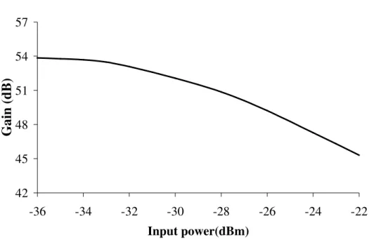
For the sake of characterizing the transmitter quantitatively, it’s worth saying that the nodes are 1185, and 98 device ports are present. Therefore the number of nonlinear components in the transmitter is relatively large: 45 FET and 8 diodes. The input 45 MHz IF carrier is phase and amplitude modulated according to the π/4-DQPSK format. The LO signal is sinusoidal with -6 dBm available power at 855 MHz. 4 LO harmonics plus one lower and one upper sideband per LO harmonic are taken into account. The total input IF power is -26 dBm, whereas the total RF power is 23 dBm; consequently, the small signal gain of the transmitter is more than 49dB, and it works at the 4-dB compression point (fig. 3.5). This operation point has been chosen in order to show the effect of the nonlinearities onto the link figures of merit.
In the end, the bit-.rate of the signal propagating through the radiolink is 48.6Kbit/s.
42 45 48 51 54 57 -36 -34 -32 -30 -28 -26 -24 -22 Input power(dBm)
G
a
in
(
d
B
)
Figure 3.5: Compression gain.
Note that a large number of nonlinear components are present in the transmitter. Besides, it’s well known that to obtain an adequate spectral resolution, ∆f, we need a large number of envelope sampling instants ∆t. In fact,
∆t N 1 T 1 ∆f s⋅ = = (3.14)
So, combining these two separate information, a consideration comes up: it’s not possible to resort to conventional HB approach to analyze the transmitter; for the sake of numerical efficiency, nonlinear analyses must carried out by a model order reduction technique based on Krylov subspaces [13].
3.3.2 TRANSMITTING ANTENNA
The transmitting antenna is a typical radiating element used in mobile communications field. It’s a planar inverted-F antenna (PIFA), which is suitable for cell phones at GSM frequencies. It has been modelled for GSM900 and GSM1800 up-link bandwidths, even if the link has been analysed only at 900MHz frequency.
The standard dimensions of the PIFA antenna have been initially calculated through the formula c) 4(b c f01 + = d) 4(a c f02 + = (3.15)
Where f01 and f02 are the resonant frequencies. Then, an optimization on other seven antenna critical parameters leads to the final results. The seven optimization variables include the shorting pin radius (the same for every pin), the feeding pin radius (one variable), the position of both the feeding pin (four variables) and the gap between the patches.
Figure 3.6 : PIFA antenna; a) perspective view; b) top view.
In fig.3.6 a) and b) a perspective and top view of the dual-band antenna are shown. The dimensions of the proposed antenna are a=50mm, b=14mm, c=32.4mm, d=24.5mm. The gap is 1mm wide.
Figure 3.7: |S11| at GSM900 bandwidth
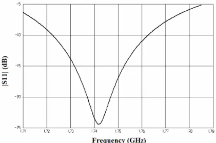
As for the performances, the targeted bandwidth at -6dB (mobile communication standard) is 890-915MHz. The requirements are fulfilled at -10dB threshold, as we can see in fig. 3.7. In fig. 3.8, the reflection coefficient in GSM1800 bandwidth is shown. The targeted bandwidth is 1710-1785MHz. and the requirements are fulfilled at -6dB threshold.
Figure 3.8 : reflection coefficient in GSM1800 bandwidth.
30 210 60 240 90 0 -20 -40 -60 -80 -100 27 0 120 300 150 330 180 0 θ rE at =0φ rE at =0φ φ
Figure 3.9: E-plane and H-plane radiation patterns of a PIFA mounted on a handset; sweep of θ angle
The typical radiated field of a patch antenna is shown by simulation in fig. 3.9. The electromagnetic tool utilized to calculate the antenna S-parameters and radiated field is the 2D and a half EM tool Ansoft Designer. The total radiated power is 220mW.
This planar antenna, designed in x-y plane, radiates in the broadside direction. The maximum of its radiated field is in the orthogonal direction θ=0, as it may be understood looking at fig.3.9.
3.3.3 RECEIVING ANTENNA
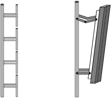
As for the receiving side, a classical vertical dipole array has been chosen (fig. 3.10). The dimension of each dipole composing the array is L =0.475λ. The gain of the proposed array is around 4.4dB , and its radiation pattern is omnidirectional in the plane orthogonal to dipole axis z (fig. 3.11). Such plane is θ=90° plane.
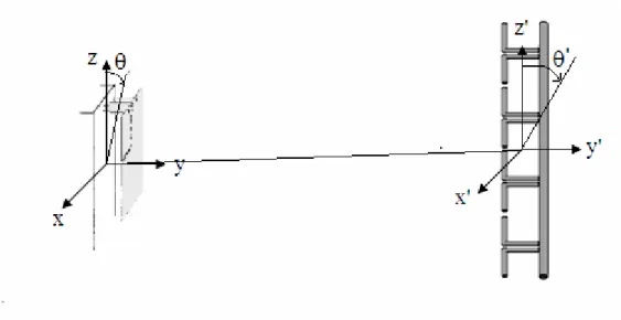
The link is calculated in one direction, which is visualized through the arrow in fig. 3.12. The PIFA antenna is rotated towards θ positive direction (90°), so that the new maximum of the radiated field can be found at θ=90°, for both the antenna systems. The distance between the antenna phase centers is 5 km, and free-space propagation is assumed.
Figure 3.10 : Receiving dipole array; a) four collinear dipoles; b) array mounted on a support
The assumption according which the link is computed only in the maximum power direction is not restrictive; in fact, a general the 3D case study of the link involves only an additional computational effort( i.e. implementation of the same method for every combination of θ and φ angles), and no further conceptual issues.
Note that in order to analyze the link in a generic condition (i.e., with an arbitrary orientation of the handset with respect to the link direction), we need not only the radiation diagrams, but also the frequency-dependent polarization and phase of the transmitted far field in any direction of space. It is then clear that EM simulation is a must whenever it is desired to take into account the effects of real-world antenna systems.
Figure 3.12: Link direction
3.3.4 RECEIVER
After the signal have been received from the 4-ports dipole array, a proper Wilkinson power combined is inserted at the section between the antenna and the receiver.
Subsequently, the receiver presents an architecture similar to that of the transmitter (fig. 3.13). The RF signal, which has total power equal to -80dBm at 900MHz, flows out from the
splits the signal in two different paths, and, before being down converted by the doubly-balanced mixer, each signal is again amplified. The mixer makes use of a 0 dBm local oscillator signal. A lumped quadrature coupler then recombines the two paths into the same signal, which is now at 90MHz intermediate frequency. In the end, the last steps consists in filtering and amplifying the IF output signal. The small signal gain of the receiver is around 60 dB, so that the RF ouput power is equal to -20dBm.
Similarly to the transmitter, the receiver has a large number of nonlinear components; 208 device ports and 1745 nodes confirm the high complexity of this nonlinear system. The analysis carried out is the same performed for the transmitter.
Figure 3. 23 : Block diagram of the receiver
3.3.5 RESULTS
Let us give now some information on simulation time. On a modern PC, the EM analysis of each antenna takes about 50 minutes, and is carried out once for all. A “local” nonlinear analysis
reduction techniques become a must in order to keep the CPU time within reasonable limits, because of the problem sizes.
Nevertheless, this reference figure could be significantly reduced thanks to recent algorithmic improvements, such as harmonic balance based on automatic domain decomposition [8]. In addition, previous experience shows that after exactly computing the system response at a number of sampling instants of the order of 100, the available information is sufficient to train a recursive neural network which is able to accurately determine the response at all subsequent instants. In this way very long bit sequences can be cheaply generated.
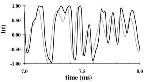
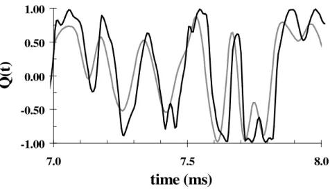
The numerical results found by means of the Co-simulation technique developed are shown in the following pictures. First of all, figs. 3.14 and 3.15 show a comparison between the in-phase I(t) and quadrature Q(t) components of the normalized signal envelopes at the transmitter input (grey line) and at the receiver output (black line). In both cases, note that the output is clearly distorted; there are two reasons explaining this phenomenon. The first has to do with nonlinearities: since both the transmitter and the receiver operate in nonlinear regions, consequently these devices distort their input signal.
-1.00 -0.50 0.00 0.50 1.00 7.0 7.5 8.0
time (ms)
I(
t)
Figure 3.14: In-phase component of the normalized signal envelopes at the transmitter input (grey line) and at the receiver output (black line)
-1.00 -0.50 0.00 0.50 1.00 7.0 7.5 8.0
time (ms)
Q
(t
)
Figure 3.15 : Quadrature component of the normalized signal envelopes at the transmitter input (grey line) and at the receiver output (black line)
The second reason regards the linear part of the link: in particular, since the antenna are frequency selective elements, every frequency of the spectrum of the signal radiated by the antenna is attenuated in a different way; the correspondent time-domain envelope shape is consequently distorted. Finally, note that the distortion presents two natures , on one side nonlinear, on the other linear respectively.
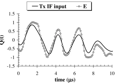
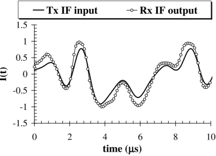
If we analyze now the shapes of the radiated field (fig. 3.16 and 3.17, black lines) for both in-phase and quadrature components, we may understand how this envelope shape is very different from the one at the input at the transmitter (fig. 3.14 and 3.15, grey lines) . Actually, the seeming disagreement is justified by the consideration that the transmitting antenna acts as a signal differentiator, as it appears looking at the ET(ω) formula [18]; in fact, the complex “j” in frequency domain corresponds to a time-domain derivative. Such derivative, traced as a grey line, has been superposed to the radiated field curve, both in fig 3.16 and 3.17 . The agreement is good, so that the above mentioned explication is demonstrated.
-1.00 -0.50 0.00 0.50 1.00 7.0 7.2 7.4 7.6 7.8 8.0
time (ms)
I(
t)
Figure 3.16: In-phase normalized input signal derivative (grey line) and radiated far-field envelopes (black line)
-1.00 -0.50 0.00 0.50 1.00 7.0 7.2 7.4 7.6 7.8 8.0
time (ms)
Q
(t
)
Figure 3.17: Quadrature normalized input signal derivative (grey line) and radiated far-field envelopes (black line)
Other figures of merit to be analyzed are the IF spectra at the transmitter input and at the receiver output. They are shown in figure 3.18 and 3.19. The input voltage spectrum shows a bandwidth equal to 48.6 KHz as expected; obviously, the signal is not distorted, and in fact no sideband can be observed in the spectrum. On the contrary, the output voltage spectrum, shows a typical nonlinear phenomenon, which is the spectral regrowth. This is due to the nonlinearities generated by both front-end and it may be quantified looking through the sidebands. Since the step between the main bandwidth and the first sideband is more than 20dB, we conclude that, as expected, the distortion is not dramatic, but not negligible.
-120 -100 -80 -60 -40 -100000 -50000 0 50000 100000 Offset(Hz) In p u t v o lt a g e (d B ))
Figure 3.18 : transmitter input spectrum
-140 -120 -100 -80 -60 -40 -100000 -50000 0 50000 100000 Offset(Hz) O u tp u t v o lt a g e (d B ))
Figure 3.19: Receiver output spectrum
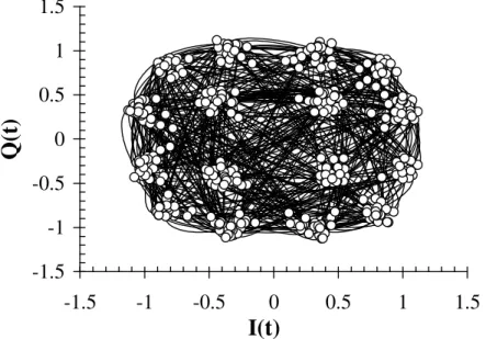
The constellations of the IF input and output signal envelopes, are shown in fig. 3.20 and 3.21 respectively. The input signal shows a clear π/4-DQPSK constellation. Because of the above mentioned distortion, the eight states of the constellation are not visible anymore at the receiver output.
-0.05 0.00 0.05 -0.05 0.00 0.05
I(t) (V)
Q
(t
)
(V
)
Figure 3.20 : Transmitter input constellation
-0.01 0.00 0.01 -0.01 0.00 0.01
I(t) (V)
Q
(t
)
(V
)
4.1
INTRODUCTION
This new chapter handles the extension of the general and rigorous link analysis method developed in the previous chapter.
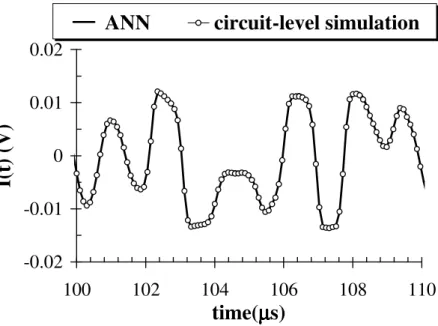
In chapter 3, full-wave EM analysis was limited to the antennas that were treated in the conventional way, i.e., as a one-port components interacting with the transceivers exclusively through their connection ports. In this way field-circuit interactions were not considered. In the next paragraphs I adopt an advanced viewpoint, whereby each antenna may be described as part of an integral linear subnetwork that interacts with environmental EM fields as a whole, thus providing a unified approach to the treatment of ordinary transmission, active and passive interference, and EM compatibility. On the transmitter side, the radiated field is directly related to the transmitter front-end state variables, so that its complex envelope may be directly computed by envelope-oriented harmonic balance when the transmitter IF input is driven by a modulated signal. On the receiver side, the connection is established by deriving the circuit-level receiver excitation through EM theory, starting from the complex envelope of the field incident on the receiver linear subnetwork, which includes the receiving antenna. This is equally valid for the desired (transmitted) field and for any other (interfering) field existing in the receiver environment. In this way the most commonplace quality indicators for the link, such as eye diagrams and power spectra (both with and without interference), can be directly computed. Special attention is devoted to bit-error-rate (BER) calculation, which poses the additional problem of exceedingly long CPU times. In chapter 3, BER calculation was not considered; in these paragraphs it is made possible by resorting to an artificial neural network (ANN) allowing the extension of a relatively short sequence of output samples generated by simulation, both in the absence and in the presence of noise.
The proposed analysis approach is validated by comparing the link performance computed by our technique with the results generated by direct time-domain analysis. This is done for a reference link whose transceivers are small enough (8 transistors overall) to fall within the reach of SPICE-like simulation. A full demonstration of the capabilities of the method is then provided by