2016
Publication Year
2020-05-21T08:37:42Z
Acceptance in OA@INAF
ASTRI SST-2M camera electronics
Title
SOTTILE, Giuseppe; CATALANO, OSVALDO; LA ROSA, GIOVANNI; CAPALBI,
Milvia; GARGANO, Carmelo; et al.
Authors
10.1117/12.2232464
DOI
http://hdl.handle.net/20.500.12386/25030
Handle
PROCEEDINGS OF SPIE
Series
9906
Number
ASTRI SST-2M camera electronics
G. Sottile
a, O. Catalano
a, G. La Rosa
a*, M. Capalbi
a, C. Gargano
a, S. Giarrusso
a, D. Impiombato
a,
F. Russo
a, P. Sangiorgi
a, A. Segreto
a, G. Bonanno
b, S. Garozzo
b, D. Marano
b, G. Romeo
b,
S. Scuderi
b, L. Stringhetti
c, R. Canestrari
d, R. Gimenes
e,
for the ASTRI Collaboration and the CTA Consortium
a
INAF - Istituto di Astrofisica Spaziale e Fisica cosmica di Palermo, via U. La Malfa 153, I-90146
Palermo, Italy
b
INAF - Osservatorio Astrofisico di Catania, via S. Sofia 78, I-95123 Catania, Italy
c
INAF - Istituto di Astrofisica Spaziale e Fisica cosmica di Milano, via Bassini 15, I-20133
Milano, Italy
d
INAF - Osservatorio Astronomico di Brera, via E. Bianchi 46, I-23807 Merate (LC), Italy
e
IAG-USP - Instituto de Astronomia, Geofísica e Ciências Atmosféricas, Universidade de São Paulo,
Rua do Matão 1226, 05508-090 São Paulo, SP, Brazil
ABSTRACT
ASTRI SST-2M is an Imaging Atmospheric Cherenkov Telescope (IACT) developed by the Italian National Institute of Astrophysics, INAF. It is the prototype of the ASTRI telescopes proposed to be installed at the southern site of the Cherenkov Telescope Array, CTA. The optical system of the ASTRI telescopes is based on a dual mirror configuration, an innovative solution for IACTs, and the focal plane of the camera is composed of silicon photo-multipliers (SiPM), a recently developed technology for light detection, that exhibit very fast response and an excellent single photoelectron resolution. The ASTRI camera electronics is specifically designed to directly interface the SiPM sensors, detecting the fast pulses produced by the Cherenkov flashes, managing the trigger generation, the digital conversion of the signals and the transmission of the data to an external camera server connected through a LAN. In this contribution we present the general architecture of the camera electronics developed for the ASTRI SST-2M prototype, with special emphasis to some innovative solutions.
Keywords: CTA, ASTRI, IACT, SiPM, Front-End Electronics, Back-End Electronics
1. INTRODUCTION
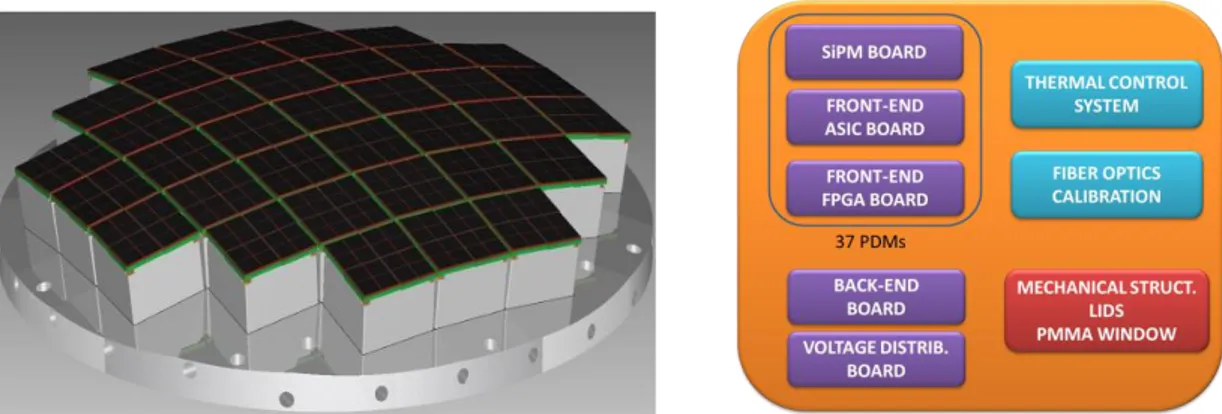
ASTRI SST-2M [1] is a Cherenkov telescope prototype developed by the Italian National Institute of Astrophysics (INAF) and proposed as one of the Small Sized Telescope (SST) options for the Cherenkov Telescope Array (CTA) observatory [2][3]. The ASTRI telescopes are based on a dual mirror optical system, an innovative solution for Imaging Atmosphere Cherenkov Telescopes (IACTs), and a focal plane composed of Silicon Photo-Multipliers (SiPM), a recently developed technology for light detection that exhibits high gain and quantum efficiency, very fast response and an excellent single photoelectron resolution [4][5]. The camera [6] is designed with an electronics that is specifically devoted to interface the SiPM detectors, catching the fast pulses produced by the Cherenkov light. The camera electronics also manages the trigger generation, the digital conversion of the signals and the transmission of the data produced to an external camera server, connected through a Local Area Network (LAN). The Schwarzschild-Couder configuration, used for the ASTRI telescopes, is a dual mirror optical system [7][8], that gives a wider field of view compared to traditional single mirror and a reduced plate scale, leading to a camera of compact dimensions which allow us to use small SiPM detectors as camera pixels. The drawback of this kind of optics is a curved focal plane and a very short depth of focus. To follow the curvature of the focal plane, the light sensors have been distributed on top of 37 Photon Detection Modules (PDMs), see Figure 1 (left panel). The dimensions of the PDMs resulted to be only 57.6mm x 57.6mm, accommodating an 8x8 matrix of pixels. Based on these constraints and in order to optimize the overall camera design, the ASTRI SST-2M camera electronics has been divided into two main systems:
the Front End Electronics (FEE), placed inside each one of the 37 PDM boxes, that directly interfaces the SiPMs, and the Back End Electronics (BEE) that collects the data produced by the 37 PDMs and distributes them to the camera server.
2. GENERAL DESCRIPTION
Before starting with the detailed description of the camera electronics subsystems, it is better to understand which are the main blocks that compose the camera electronics. Figure 1 (right panel) shows a high level block diagram.
The ASTRI SST-2M camera electronics is composed of 37 PDMs containing the FEE, the BEE board where there is the main logic that manages the camera functions, the Voltage Distribution Board (VDB) that provides all the required regulated voltages to the 37 PDMs, the Thermal Control System (TCS) that stabilizes the focal plane temperature, and the Fiber Optics Calibration (FOC) system that allows the relative calibration of the focal plane pixels.
Each PDM contains three boards. The top board accommodates the SiPM light sensors in a matrix of 8x8 pixels and 10 temperature sensors. The middle board contains two 32 channels Application Specific Integrated Circuits (ASICs) that directly interface the 64 SiPMs of the PDM; the ASICs have 2 multiplexed outputs connected to a separate Analog-to-Digital Converter (ADC) that converts the signal of each ASIC channel. The ASICs also provide discriminator outputs, one for each channel, that are used to produce a local trigger. The bottom board hosts a Field Programmable Gate Array (FPGA) that implements the algorithm for the generation of the local trigger, the logic for event acquisition and the transmission of the data produced to the BEE.
Figure 1. Left: A rendering of the curved focal plane, showing the arrangement of the 37 PDMs. Right: High level block diagram of the ASTRI SST-2M prototype camera electronics, showing the main components.
The BEE is hosted on a separate common board. The heart of the BEE is a FPGA with a System on Chip (SoC) running an operating system that manages the overall camera functions. The BEE is connected to a control room through 2 LAN connections, allowing to receive commands from a camera controller and to send data packets to a camera server. The BEE is also connected to some ancillary subsystems, inside the camera, to control the opening and closure of the camera lids, the thermal regulation system, the voltage regulation and distribution, the calibration system and the Global Positioning System (GPS). Finally the BEE receives data from several sensors to monitor the temperature and the humidity inside the camera.
The VDB generates and distributes the required operating voltages to the 37 PDMs starting from a single 24V power supply. This includes low voltages to power the ASIC board and the FPGA board plus the high voltage (30-75V) to bias the SiPM sensors.
The TCS provides the thermal control of the SiPM sensors of the focal plane, stabilizing and equalizing the SiPM temperature all along the focal plane. This is accomplished by a suitable Peltier Cell which cools (or heats, depending on the environmental conditions) the focal plane support structure that holds the PDMs boxes.
The FOC system is realized by illuminating, with a Light Emitting Diode (LED), one end of a side glowing fiber optic, placed all around the focal plane perimeter. When the LED is pulsed, it illuminates the whole focal plane allowing relative calibration of the SiPM pixels. This operation can be performed even during nominal scientific observation.
3. THE PHOTON DETECTION MODULE
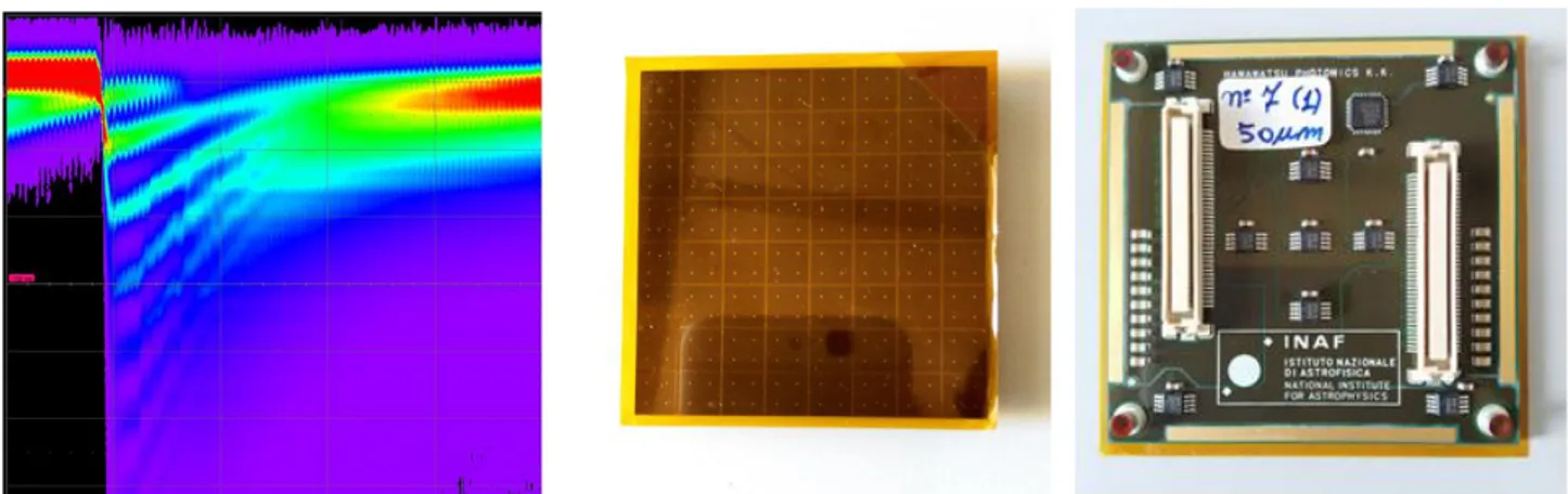
The focal plane of the ASTRI SST-2M camera is composed of 37 PDMs, each one composed of three electronics boards to form a stack architecture: the SiPM board, the ASIC board and the FPGA board. Figure 2 shows the stack architecture of the PDM. This stack is contained in an aluminum box.
Figure 2. The stack architecture of the PDM (upside-down): from top to bottom, there is the FPGA board, then the ASIC board and then the SiPM board. The dimensions are 57.6mm x 57.6mm, with a depth of 30mm.
The top element of that stack is composed by a matrix of 8x8 SiPM pixels mounted on a board, on the bottom of which there are two connectors to interface the underlying ASIC board. SiPMs are recently developed light detectors that offer very attractive performance: excellent single photon resolution (see Figure 3 left panel), excellent timing (hundreds of picoseconds), high photon detection efficiency (>30% at the peak), low bias voltage (30-100V), no damage when exposed to ambient light, insensitivity to magnetic field. At the beginning of their development, SiPMs had some troublesome drawbacks: very high dark counts (~1MHz/mm2 ), after-pulses (~20%), optical crosstalk (~20%), gain strongly dependent on temperature and sensitive to red light, where most of the Night Sky Background is concentrated. Nowadays the manufacturers have greatly reduced the dark counts to a level of 60KHz/mm2, well below the photon rate due to Night Sky Background in moonless conditions. The optical cross-talk and the after-pulses have also been reduced at level of few percent [9].
Figure 3. Left: A collection of SiPM pulses, showing the excellent photoelectron resolution. The signal pulse shows an ultra-fast leading edge (hundreds of picoseconds) followed by a trailing edge with an exponential decay (50ns in this case).
Center: Top view of the SiPM board (covered by a protective foil) where it is visible the 8x8 matrix configuration of the
The SiPM boards for the ASTRI SST-2M prototype were produced by Hamamatsu under custom design, in order to match the dimensions of the pixel (7mm x 7mm) with the Point Spread Function (PSF) of the optical system of the telescope. The SiPM used in the boards belongs to the latest family of Low Cross Talk (LCT) technology. The SiPM boards also contains 10 sensors to monitor the SiPM operating temperature.
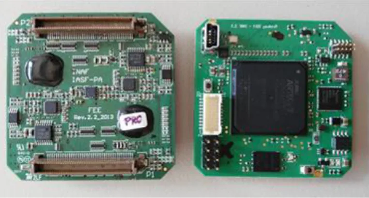
The ASIC board is placed in the middle of the PDM stack, between the SiPM board and the FPGA board. The model of the ASIC used for the ASTRI SST-2M prototype is the Cherenkov Imaging Telescope Integrated Read Out Chips (CITIROC) produced by WeeROC [10], with partial INAF intellectual property. The CITIROC is the most important component of the FEE. It directly interfaces the SiPM sensors providing, at outputs, both event amplitude and trigger signals for each input channel, i.e. for each pixel. The trigger signals are sent to the FPGA board, where they undergo a special topologic algorithm that sets a flag, PDM TRIG, when 5 or more adjacent pixels are hit. The PDM TRIG signal is then sent to the BEE that, in turn, routes back to all the PDMs of the focal plane a logic signal, CAMERA TRIG, to start the event capture simultaneously all over the focal plane. The amplitude signals are then converted on-board by a 12-bit ADC and then sent to the FPGA board where they are forwarded to the BEE for subsequent data processing.
Figure 4. The ASIC board (on the left) and the FPGA board (on the right). The ASIC board shows the side where there are placed the two ASICs (covered by resin) and the two ADCs with their relevant preamplifiers. The FPGA board shows very few components and the connectors for power (to the VDB) and signals (to the BEE), and a USB to be used during lab tests.
The FPGA board has in charge the whole management of the FEE inside a PDM. The FPGA used is an ARTIX 7 model, produced by Xilinx. The firmware is composed by several modules (see Figure 6) each one performing a dedicated task: Trigger Flag Generation, ASIC configuration through a slow control line, acquisition mode control, reading of the data converted by ADCs, housekeeping collection and clock generation. Moreover inside the FPGA it is implemented a microprocessor (uBLAZE) running a software with the main function of command parser. It receives commands from the BEE during normal operations, and from a Personal Computer connected through a USB, during PDM stand-alone tests.
There are basically two techniques used to acquire SiPM pulses: sampling and shaping. The first method samples the SiPM signal at very high speed (~0.5-1GHz), the shaper, instead, integrates the pulses with a certain shaping time constant (~50ns). We tested the CITIROC performance and characteristics by means of a long test campaign in laboratory and only after it fulfilled the requirements, it was chosen for the project. CITIROC is a shaper that exhibits very attractive features: very low power (300mW/chip), low data transfer per event (just 2 values/pixel/event), one discriminator output per pixel, suitable for topologic trigger generation and, the most important, each input of the ASIC is connected to an internal Digital-to-Analog Converter (DAC) to fine tuning the bias voltage of each pixel (see Figure 5 left panel); in this way a precise gain equalization can be obtained with just one high voltage (HV) generator per PDM. All those characteristics were not found in the samplers on the market, at the time of the design.
Other CITIROC characteristics are: 32 input channels with separate chain for high gain (HG) and low gain (LG), 32 separate trigger outputs, high dynamic range of measurement: 160fC÷320pC (1:2000 photoelectrons at SiPM Gain=106) using both chains, input preamplifiers with variable gain, HG/LG slow shapers with variable time constant (12.5÷87.5ns), common 10-bit DAC for coarse threshold setting, plus a 4-bit DAC per pixel for fine tuning of the threshold, peak detector mode (to stretch the peak of the slow shaper), HG/LG multiplexed outputs [11][12].
Figure 5 (right panel) shows the block diagram of the CITIROC ASIC. On top left (box A), there are the two input preamplifiers, AC coupled, one for the high gain and the other for the low gain, together with the input DAC that is one of the most important features of this chip, because it allows the fine regulation of the bias voltage of the SiPM pixel connected to that input, allowing an easy way to equalize the gain of all the pixels of the focal plane.
Figure 5. Left: Schematic of the connection of a SiPM pixel to the relevant CITIROC input. It shows also the important function of the input DAC inside the CITIROC. Right: The CITIROC block diagram (explained in the text).
On top center (box B), there are the two slow shaper chains. In the center (box C), there is a fast shaper followed by a double discriminator chains. The time trigger outputs of those discriminators are sent to the FPGA, where they are used to generate a PDM trigger. On the bottom (box D), there is the part of circuit common to all the 32 channels. On the right (box E), there are the multiplexed outputs for the signal amplitude and the parallel outputs of the 32 discriminators.
Figure 6 shows the PDM block diagram. The signals of the 64 SiPM pixels are injected to the CITIROC inputs (32+32). At the end of the shaping time the peak value of the shapers are hold by a peak detector circuit. Then the conversion starts in 4 ADCs channel by channel, sequenced by two multiplexer per ASIC (high gain and low gain). The FPGA is in charge to manage the operating mode of the PDM: configuring the ASICs by means of some logic control lines, starting the conversion upon reception of the CAMERA TRIG signal, and subsequently reading the data produced. Moreover, inside the FPGA it is implemented an algorithm for the generation of a topological trigger, the PDM TRIG.
4. BACK-END ELECTRONICS
The Back End Electronics is the read-out part of the ASTRI SST-2M camera electronics. The heart of this board is a powerful FPGA that manages the whole camera functions. The main BEE tasks are: trigger signal routing, clock distribution, event time tag, events storage in a local memory, data packing and transmission, interface (I/F) to the FEE (PDM), I/F to the external camera control and camera server, operating modes management, ancillary equipment control.
Figure 7. Left: The Back End Electronics. The board dimensions are 220mm x 250mm. Right: Block diagram of the BEE showing the architecture designed for ASTRI SST-2M as implemented inside the Zynq FPGA. The ancillary subsystems controlled by the BEE are also highlighted. On the left, there are the signals that interface each PDM. On the right, there are the LAN links that allows the communication to the external world: the Camera Control and the Camera Server.
The FPGA used for the BEE is a Xilinx Zynq [13]. This family of FPGAs integrate the software programmability of an ARM®-based processor with the hardware programmability of an FPGA, enabling hardware acceleration while integrating mixed signal functionality on a single device. The presence of a System on Chip (SoC) avoids the installation of a separate microprocessor on board of the BEE. The Zynq FPGA is then subdivided into two parts: a Processing System (PS) that runs the operating system and the camera software and the Programmable Logic (PL) where it is placed the hardware logic of the BEE. The two subsystems communicate through a shared memory, so that the software running on the PS can have access to the data and signals of the PL, see Figure 7 (right panel).
The BEE interface to the external world is obtained through two LAN lines. The first LAN connection is devoted to receive commands from a Camera Control, thus configuring the camera to one of the programmed operating modes on the basis of the observation or calibration to be executed. The second LAN connection is used to send data packets to a Camera Server. This is a high speed link working on UDP protocol, for the prototype. The TCP/IP protocol is under study to assess whether it can be used in the case of the ASTRI mini-array of CTA pre-production telescopes. A detailed description of the BEE software is given in a contribution of this proceedings [14].
On the other side, the BEE is interfaced to each of the 37 PDMs through some logic signals and serial lines. There is a slow serial line (UART) that is used to send commands to the PDMs. These commands can be directed to a single PDM or broadcasted to all the PDMs at the same time. There are commands to set the configuration of the CITIROCs and the registers of the PDM-FPGA, allowing a variety of acquisition modes suitable for observations as well as for calibrations. Two logic lines are very important: PDM TRIG and CAMERA TRIG. When the BEE receives a PDM TRIG from one of the PDMs, it routes back this trigger signal to all the PDMs so that the acquisition of an event can start in all the PDMs of the focal plane. At the end of acquisition the PDMs send their data to the BEE through a fast serial line, using the SPI protocol. The data received by the BEE are then packed and sent to the Camera Server. The routing of the PDM TRIG is foreseen to undergo a decision algorithm that could be used for zoned trigger, thus vetoing the trigger for unwanted PDM combinations.
Each of the PDMs is connected to the BEE through 8 digital signals. All the connections are realized with differential lines to minimize the noise that can be picked up or emitted by all other wires in the camera. This means that the BEE has to buffer nearly six hundreds of signals. The Zynq chip package doesn’t have such a huge number of I/O pins. The use of external discrete buffers leads to a prohibitive population of chips on-board of the BEE. The problem was solved introducing two more FPGAs used, almost exclusively, to buffer the signals between the BEE and all the PDMs. As pointed out in Paragraph 2, the BEE is also in charge to control all the camera subsystems. These are: the VDB that provides regulated voltages to all the PDMs, the TCS that stabilizes/equalizes the SiPM sensor temperatures by means of suitable Peltier cells, the motors that open and close the camera lids, the calibration LEDs, the calibrated photodiode and a commercial GPS board that provide the UTC time and the synchronization for time tagging of the events.
In order to interface all of the subsystems, different I/F protocols have been implemented inside the BEE: USB, RS232, RS485, I2C and SPI.
5. ANCILLARY EQUIPMENT
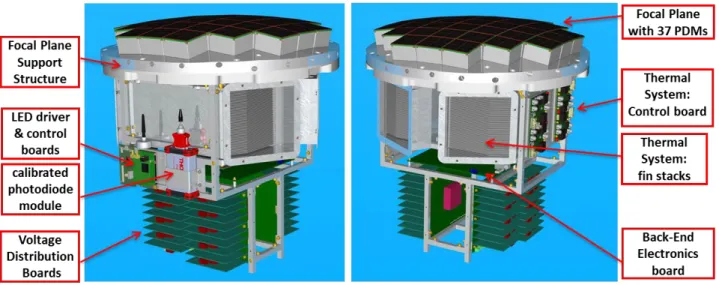
Beyond the FEE and the BEE, the ASTRI SST-2M camera is completed by a certain number of subsystems that perform special functions. The list of those subsystems is already given in the above text. In this paragraph we provide some further information for a few of them. Figure 8 shows the positions of the ancillary equipment.
Figure 8. Here are shown two rendering of the inner of the ASTRI camera, taken from a different point of view. The assembly is very compact. There are indicated the position of the most important parts of the camera.
One of the most important subsystem is the VDB. This is the equipment that provides the correct regulated voltages to all PDMs. Because of the very small dimensions of the boxes hosting the PDMs, it was necessary to move the relevant power circuitry away from the PDMs. The VDB is composed of two mainboards, each one accommodating 19 daughterboards. The two mainboards are connected to the BEE in a daisy-chain way. The BEE is in charge to control all
the functions of the VDB. The BEE can command the switching ON/OFF of each single voltage, as well as their value (in a limited range). The regulated voltages produced by each daughterboard are: +5.5V, +3.6V, -3.3V to power the ASIC board, +7V to power the FPGA board and a high voltage (35-75V depending on the SiPM technology used) to bias the SiPM sensors. All the outputs are protected against short circuit or excessive current. In particular the high voltage is, as a precaution, switched-on following a slow rising ramp.
As the gain of the SiPM is strongly dependent on temperature, it became necessary to realize a thermal control system to maintain at a fixed value the temperature of all the sensors, and this temperature is also equalized all along the focal plane. This was realized with Peltier cells that provide the temperature stabilization and with heat pipes embedded in the focal plane support structure to act as a thermal short circuit for the whole focal plane.
The FOC subsystem that allows the relative calibration of the pixels is realized using a side glowing optical fibre surrounding the focal plane. One end of this fiber is illuminated by a LED and on the other end it is placed a calibrated photodiode to monitor the light level emitted by the LED. The SiPM sensors are illuminated by the light exiting the optical fiber and partially reflected back by the Poly Methyl Metha Acrylate (PMMA) window that protects the focal plane from the external environment. The BEE provides the strobe for the LED pulse and, at the same time, it reads back the light received by the calibrated photodiode. This operation can be executed during calibration as well as during a nominal observation window, at specific time interval.
6. OPERATIONAL CONCEPT
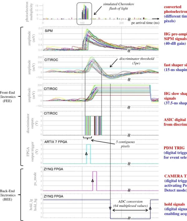
We describe here the flow of operations which undergo in the ASTRI SST-2M camera electronics when a Cherenkov flash reaches the focal plane. When a photon hits a SiPM pixel and it’s absorbed, then an electrical pulse is generated and the signal is fed into the FEE. Each pixel of the focal plane is directly connected to one of the inputs of the front-end ASIC.
CITIROC is used as front-end inside the ASTRI SST-2M camera electronics. Each CITIROC input is internally split in two electronic chains, one for the low gain and the other one for the high gain. The input preamplifiers are AC connected to decouple them from the input DAC that is used to fine adjust the SiPM bias voltage. Each preamplifier is followed by a slow shaper with programmable shaping time (12.5-87.5ns) and then there is a circuitry that can work in tracking mode or in peak detection mode. At this step, the signal amplitude is stored for the subsequent conversion by an ADC. The choice of the appropriate shaping time is a trade-off between two aspects. It should be as short as possible to minimize the collection of unwanted pulses, like those coming from Night Sky Background or detector noise. On the other hand, the time constant should be long enough to fully integrate the signal of the genuine Cherenkov event that could last up to tens of nanoseconds, depending on various elements. A third electronic chain is derived from the output of the high gain input preamplifier. This signal is routed to the input of a fast shaper (15ns) whose output goes to a discriminator. When the fast shaper signal overcomes a pre-defined threshold, the discriminator generates a trigger signal that, in turns, is sent to the FPGA Board. This process is shown in Figure 9. All the pixels, in a PDM, that produce a signal in the fast shaper that overcomes the threshold generate a trigger signal that is sent to the FPGA.
In a PDM, all the 64 discriminators are connected in parallel to the FPGA where an algorithm will generate a PDM trigger signal (PDM TRIG). The trigger algorithm works as follow: when the FPGA receives active trigger signals from five contiguous pixels, in any position of the PDM, it generates the PDM TRIG and sends it to the BEE.
The BEE electronics routes the PDM TRIG signal received by one PDM (or more) back to all the 37 PDMs of the focal plane (CAMERA TRIG), thus activating the peak detectors inside the CITIROCs. As soon as the peak detection becomes active, an integration window starts in the two slow shaper electronic chains. The peak detector maintains the output at the maximum value reached during the integration time. At the end, the peak detector input is opened and the acquisition starts for all the CITIROC channels. When the transmission ends, the BEE releases the CAMERA TRIG signal changing back the operating mode from peak detection to tracking and the PDM is then ready to capture the next incoming event.
The CAMERA TRIG signal is time tagged and included inside the data packets transmitted to the Camera Server. Inside the ASTRI SST-2M camera prototype, a GPS receiver provides the UTC time and a precision pulse-per-second to synchronize the internal clock. In the future, and for the ASTRI pre-production CTA telescopes, other time synchronization systems will be tested, in agreement with the CTA Collaboration indications.
The digitization of all the CITIROC outputs takes ~8µs whereas the transmissions of the data to the BEE lasts ~21µs. This means that the instrument is busy for 29µs per event. Considering an event rate of 600/s, then the estimated dead time of the ASTRI SST-2M camera will be less than 2%.
PDM TRIG
(digital trigger pulse for event selection)
HG pre-amplified SiPM signals
(40-dB gain)
CAMERA TRIG
(digital trigger pulse activating Peak Detect mode)
ASIC digital signals from discriminators Front-End Electronics (FEE) Back-End Electronics (BEE) hold signals (digital signal enabling acquisition) converted photoelectrons
(different time and pixels)
fast shaper signals
(15-ns shaping time) HG slow shaper signals (37.5-ns shaping time) discriminator threshold ADC conversion (64 multiplexed values) simulated Cherenkov flash of light p h o to el ec tr o n mu lt ip li ci ty 5 contiguous pixels pe arrival time (ns) h o ld _ lg h o ld _ h g p s_ mo d e amp li tu d e (mV ) amp li tu d e (mV ) amp li tu d e (mV ) d is cr imi n at o r o u tp u ts (V) F P G A o u tp u t tr ig g er (V) (5pe)
Figure 9. A simulation of the FEE signals where it is possible to follow the temporal sequence of the signals involved when an event hit a PDM: from the signal generated by the fired pixels (SiPMs) up to the BEE reaction to the PDM trigger.
7. ADDITIONAL FEATURES
The flow described in the previous sections is the nominal event acquisition mode. However the PDM has two more special features that help the calibration and the observation phase.
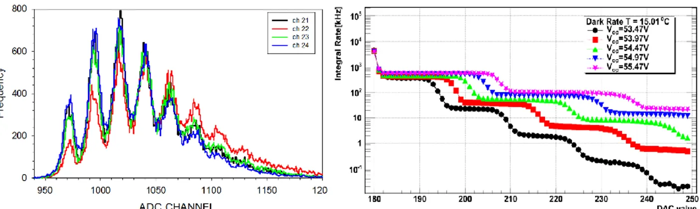
CITIROC is not designed to be used as a counter, because along the path of the trigger circuitry there is a 15ns shaper. Anyway, we noted that for low count rate (<5 MHz) the trigger pulses can be counted. This feature is used during calibration to verify the equalization of the gain and of the threshold of all the pixels in a PDM. This is obtained by swapping the discriminators threshold at very low light level or in dark so to generate a staircase plot of the trigger counts vs. trigger thresholds. Those kind of plots are typical of the SiPM sensors and provide important information about the device under test, see Figure 10 (right panel).
It is not possible for an AC coupled front-end to measure the night sky background level of light. However there is a way to bypass this limitation. By statistics consideration, the variance of the signal is proportional to its amplitude. This is accomplished by continuously sampling the front-end pedestal of each pixel, saving in two separate registers the sum of the samples and the sum of the squares of the samples, for a predefined number of samples, after which the registers are sent to the camera server where the variance is calculated. This task is implemented inside the FPGA of the PDM. When this feature is enabled, the pedestal is sampled in free-run until a CAMERA TRIG signal aborts the last sample and starts the standard event acquisition. At the end of the event acquisition the free-run sampling of the pedestal restarts.
Figure 10. Left: Gain equalization of four camera pixels after the correction of the SiPM bias voltage obtained adjusting the input DAC voltages. Right: Staircase plots taken at different gain. The inflection points separate the count rates due to n-photoelectrons to n+1-photoelectrons. The leftmost step shows the count rate due to a single photoelectron, the next one shows the count rate due to two coincident photoelectrons etc. The distance between the steps corresponds to the SiPM gain and it increases as the bias voltage raises.
8. CONCLUSIONS
The aim of this paper is not to provide a detailed analysis of the ASTRI SST-2M camera electronics, because this is matter of a technical design report that is beyond the scope of these conference proceedings. Our goal is to describe the basic architecture of the project and some of the innovative ideas used in ASTRI SST-2M prototype.
The first thing to consider is the sensors used to populate the focal plane. It’s not the very first time that SiPMs are used at the focus of a Cherenkov telescope [15] but this is the first time they are used without any light collection system (Winston cone), thus avoiding any light loss. In the present case the pixel has the same dimension of the sensor. This was possible using sensors without dead space in the middle. These sensors have been developed only recently by Hamamatsu and the dead space was eliminated by connecting the sensitive layer to the bottom pins through, what is called, Through Silicon Vias. It is worth to mention that other groups, inside the CTA project, are currently developing cameras based on SiPM sensors [16][17].
Another important thing is the complete separation of the FEE w.r.t. the BEE. Placing the FEE just below the SiPM sensors allowed us to avoid a forest of wires conducting very low voltage analog signals between the sensors and the relevant FEE. Moreover, by dividing the focal plane into separate modules, it is possible to test each module in stand-alone mode; and this helps a lot in the maintenance of the camera.
Of course this miniaturization was possible thanks to the big improvement in microelectronics that allowed the production, for CITIROC, of a chip of 5mm x 5mm (naked).
CITIROC revealed to be an ASIC suitable for interfacing the SiPM sensors. The use of a shaper that integrates the signal with a certain time constant produces data of quality comparable to the vastly used samplers with the advantage of a small amount of data transferred to the BEE per event. With this chip it is possible to easily reach a very good equalization of the gain of the sensors using the input DACs, see Figure 10 (left panel). The trigger thresholds can be fine-tuned among the pixels of the whole focal plane. This feature provides a considerable simplification of the procedures for parameters optimization and calibration. Moreover the availability of all 64 discriminator outputs allows us to use CITIROC as a counter (but only at very low light level) and obtaining the staircase plots from where it is possible to verify the gain and the equalization of the thresholds of all the pixels in the PDM.
Among the tasks performed by the front-end FPGA, it is very important the continuous sampling of the pedestal to evaluate, every second, the variance of the samples and hence the average light hitting each pixel of the focal plane. Currently the camera is under integration and it will be mounted on-board of the telescope structure at the beginning of September 2016. The ASTRI SST-2M prototype telescope, whose structure and mirrors were inaugurated in September 2014, is installed in Italy at the INAF “M.C. Fracastoro” observing station, located in Serra La Nave (Mt. Etna, Sicily)[18]
ACKNOWLEDGMENTS
This work is supported by the Italian Ministry of Education, University, and Research (MIUR) with funds specifically assigned to the Italian National Institute of Astrophysics (INAF) for the Cherenkov Telescope Array (CTA), and by the Italian Ministry of Economic Development (MISE) within the “Astronomia Industriale” program. We acknowledge support from the Brazilian Funding Agency FAPESP (Grant 2013/10559-5) and from the South African Department of Science and Technology through Funding Agreement 0227/2014 for the South African Gamma-Ray Astronomy Programme. We gratefully acknowledge support from the agencies and organizations listed under Funding Agencies at this website: http://www.cta-observatory.org/. This paper has gone through internal review by the CTA Consortium.
REFERENCES
[1] Pareschi, G. et al. for the CTA Consortium, “The dual-mirror Small Size Telescope for the Cherenkov Telescope Array”, Proc. 33rd ICRC, arXiv:1307.4962 (2013).
[2] Acharya, B. S. et al., The CTA Consortium, “Introducing the CTA concept”, Astroparticle Physics 43, 3-18 (2013).
[3] Pareschi, G., Bonnoli, G., Vercellone, S., on behalf of the ASTRI Collaboration and for the CTA Consortium, “The mini-array of ASTRI SST-2M telescopes, precursors for the Cherenkov Telescope Array”, Proc. 14th TAUP 2015 (2016).
[4] Buzhan, P., et al., “Silicon Photomultiplier and its Possible Applications”, Nucl. Instr. and Methods in Physics Research A, vol. 504, 48-52 (2003).
[5] Bonanno, G., et al., “Advances in Silicon Photomultiplier Technology: First Characterization Results”, Nucl. Instr. and Methods in Physics Research A, 794, 185 (2015).
[6] Catalano, O., et al., for the ASTRI Collaboration and the CTA Consortium, “The camera of the ASTRI SST-2M prototype for the Cherenkov Telescope Array”, Proc. SPIE 9147, doi: 10.1117/12.2055099, (2014).
[7] Vassiliev, V., Fegan, S., Brousseau, P., “Wide field aplanatic two-mirror telescopes for ground-based gamma-ray astronomy”, Astroparticle Physycs, vol.28-1, 10-27 (2007)
[8] Rousselle, J., et al., for the CTA Consortium, “Schwarzschild-Couder telescope for the Cherenkov Telescope Array: Development of the Optical System”, Proc. 33rd ICRC (2013).
[9] http://www.hamamatsu.com/resources/pdf/ssd/s13360-2050ve_etc_kapd1053e.pdf
[11] Impiombato, D., et al., “Characterization and performance of the ASIC CITIROC front-end of the ASTRI camera”, Nucl. Instr. and Methods in Physics Research A, 794, 185 (2015).
[12] Impiombato, D., et al., “Temperature characterization of the CITIROC front-end chip of the ASTRI SST-2M Cherenkov camera”, this Proceedings (2016).
[13] http://www.xilinx.com/products/silicon-devices/soc/zynq-7000.html
[14] Sangiorgi, P., et al., “The software architecture of the camera for the ASTRI SST-2M prototype for the Cherenkov Telescope Array”, this Proceedings (2016).
[15] Bretz, T., et al., “FACT – The first G-APD Cherenkov Telescope: Status and Results”, Proc. 33rd ICRC, arXiv:1308.1512, (2013).
[16] Daniel, M.K., et al., for the CTA Consortium, “A Compact High Energy Camera for the Cherenkov Telescope Array’, Proc. 33rd
ICRC, arXiv:1307.2807, (2013).
[17] Vassiliev,V., et al., for the CTA Consortium, “Schwarzschild-Couder telescope for the Cherenkov Telescope Array: 9.5m telescope prototype development”, Proc.33rd ICRC, (2013).
[18] Maccarone, M.C., Leto, G., et al, for the ASTRI Collaboration, “The Site of the ASTRI SST-2M Telescope Prototype”, Proc.33rd ICRC, arXiv:1307.5139 (2013)