Low-frequency noise spectroscopy as an effective
tool for electric transport analysis
Costantino Mauro
A Dissertation submitted to the
Dipartimento di Fisica “E.R. Caianiello”
Facoltà di Scienze Matematiche Fisiche e Naturali
in fulfillment of the requirements
for the
Doctoral degree in Physics
in the
Università degli Studi di Salerno
under the Supervision of
Prof. Sergio Pagano
Doctoral Student XXX Cycle (2015–2017)
Head of the School: Prof. R. Scarpa
"Books are a way of being fully human"
Contents
INTRODUCTION ... 1
CHAPTER 1 ... 3
Noise theory: a brief overview ... 3
1.1 Noise spectral density measurements... 6
1.2 Noise and electrical dc measurements: experimental setup ... 7
CHAPTER 2 ... 11
Noise properties and transport in aging-induced degraded iron-based superconductors ... 11
2.1 Materials and methods ... 11
2.2 DC electrical transport properties ... 12
2.3 Noise spectral density measurements... 14
CHAPTER 3 ... 19
Noise properties and transport in different polymer/carbon nanotube composites ... 19
3.1 Materials and methods ... 19
3.2 DC electrical transport properties ... 20
3.3 Noise spectral density measurements... 22
3.4 Fluctuation induced tunneling model applied to noise processes .... 24
CHAPTER 4 ... 27
Noise properties and transport in crystalline silicon-based solar cells ... 27
4.1 Materials and methods ... 28
4.2 Noise model of solar cells ... 28
4.3 Noise spectral density measurements... 32
CHAPTER 5 ... 41
Noise properties and transport in polymer:fullerene solar cells ... 41
5.1 Materials and methods ... 42
5.2 DC electrical transport properties ... 43
6.3 Noise spectral density measurements... 57
CHAPTER 7 ... 73
Conclusions ... 73
Acknowledgments ... 75
Bibliography ... 77
List of publications and presentation ... 83
Published papers ... 83
1
INTRODUCTION
It is a notable fact of nature that processes varying with time in an extremely complicated way often lead to observable averages that follow simple laws: the fast irregular collision of a piston by gas molecules, when integrated by the inertia of the piston, causes the piston to move smoothly in a motion described by Boyle's law. Similarly, the instantaneous current fluctuations in a resistive circuit average out to Ohm's law. The intensity of these fluctuations depends on materials, device type, its manufacturing process, and operating conditions. Noise, that is fluctuation is a manifestation of the thermal motion of matter and discreteness of its structure [1]. For example, in a circuit having a potential barrier such as a rectifying junction in a diode, the current is restricted to those electrons that have sufficient thermal energy to surmount the barrier. As a result, the current fluctuates in a way that is determined by the thermal fluctuations in the position and energy distribution of the electrons, producing a particular noise, called shot noise.
The introduction of the concept of noise and development of the physics of fluctuations is one of the conquest of twentieth-century physics. The early steps date back to '20s of XIX century. The English botanist Robert Brown, under microscope, observed the endless dance of pollen particles in aqueous suspension. The same happened later with mineral and smoke particles.
Only the kinetic theory of gases, in the latter part of the nineteenth century, correctly explained the Brownian movement as thermal molecular motions in the liquid environment of the particles. Moreover, the quantitative description of the Brownian motion of a particle was resolved in 1905 by Einstein.
Over time, physicists have developed special techniques for dealing with the way in which these macroscopic regularities arise from microscopic systems. For example, a monatomic gas in a cylinder is completely determined if the three position coordinates and the three momentum coordinates are specified for each of the N molecules at some instant called the initial time.
The basic idea of statistical mechanics is to replace the evolving system by an appropriate ensemble of systems, abide by the same equations of motion but having different initial microstates x.
The investigation of fluctuation phenomena, which may be called "fluctuation spectroscopy", is a valuable tool for the study of kinetic processes in matter, often much more sensitive than the measurement of mean quantities. The required measurement instrument, i.e. the "magnifier" companion is the spectrum analyzer, which acts as a microscope: it enables the visualization and measuring of voltage fluctuations, giving information on the conduction mechanisms and the dynamic behaviors of the charge carriers in the investigated systems.
In this work, several experiments and analyses performed on a broad typology of materials and compounds are presented. Structural, DC electrical
transport and noise properties are exposed for each investigated sample, and theoretical models and possible explanations of the experimental results are given to unravel physical phenomena. In particular, in Chapter 2, two distinct types of iron-chalcogenide superconductors are investigated, in their pristine and aged state, suggesting the more likely mechanism which generates the resistance fluctuations and resorting to Weak Localization theory. In Chapter 3, for the polymer/carbon nanotubes composites, the fluctuation-induced tunneling model is introduced to explain the measured temperature dependence of the electrical conductance and the I-V curve behaviors. The model can be also used to describe the resistance fluctuation processes (noise), confirming the dominant role of the intergranular tunneling processes [1]. In Chapter 4, noise spectroscopy is the swiss knife for the extraction of several parameters, which are then applied to a noise model for the evaluation of defect states in silicon based solar cells. In Chapter 5, the recombination kinetics in polymer:fullerene solar cells are investigated, shading light on the influence of the solvent additives on the temperature behavior of charge carrier transport. In the last chapter, noise measurements prove the existence of a structural phase occurring within the perovskite compound and highlight the correlation between electronic defect states distribution and device performance.
All the experiments and the noise measurements were carried out in the laboratory of the Physics Department, University of Salerno, Fisciano (Italy), under the supervision of the Prof. Sergio Pagano and Dr. Carlo Barone.
3
CHAPTER 1
N o i s e t h e o r y : a b r i e f o v e r v i e w
Noise or fluctuations are spontaneous stochastic (random) variations of physical quantities in time, that is, random deviations of these quantities from some mean values that are either constant or evolve nonrandomly in time. Then, it is clear that noise is a random process. For example, the random character of the fluctuations in solids is a consequence of the fact that thermal motion and quantum transition of particles (electrons and atoms) are random.
Being noise a stochastic phenomenon, it is necessary to deal with probability, its concepts, properties and mathematical tools.
By definition, a random process is a random function x(t) of an independent variable t, representing the time.
The distribution function of the n-th order for the given random process x(t) is defined as
1 1 1 1
( , ; ; , )
{ ( )
; ; ( )
}
n n n n n
W x t
…
x t
=
P x t
≤
x
…
x t
≤
x
(1.1)whit xi the value of the random quantity at the time ti, and P{...} the
probability of the considered event, indicated in the curly brackets.
Under the hypothesis that Wn (x1 , t1 ;....; xn , tn) are differentiable functions of
the variables x1 ,...., xn, the corresponding probability density functions can be
defined as
{
}
1 1 1 1 1 1 ( , ; ; , ) ( ) ;...; ( ) n n n n n n w x t … x t =P x ≤x t < +x dx x ≤x t <x dx+ (1.2)The first-order central moment (i.e. the mean value) of the random variable
x(t) is e expressed as 1
( )
( )
( )
( , )
x t
+∞x t dW x
+∞dx xw x t
−∞ −∞〈
〉 =
∫
=
∫
. (1.3)Following, the second-order central moment is the variance (i.e., the mean value of the fluctuation squared). The r-th order central moment is the average value of the random quantity (δx(t))r, whit δx(t) = x(t) - <x> the deviation of the
random quantity x(t) from its mean value <x> , that is the fluctuation
( )
1[ ( )]
δ
x t
r +∞dx x w x t
( )
δ
r,
−∞
At this point, a useful concept can be introduced: the correlation function. If the probability density wn (x1 , t1 ;....; xn , tn) is known for different times t1 ,...., tn,
the correlation function can be computed as
1 1 2 1 1 1
( ) ( )n n n n( , ; ; , )n n
x t x t dx dx dx x x w x t x t
δ δ δ δ
〈 … 〉 =
∫
… … … (1.5)It is one of the distinctive sign of a random process since it is a nonrandom property of the kinetics of the random fluctuations: it describes how the fluctuations δx(t) evolve in time on average.
A fundamental distribution is the Gaussian (i.e. normal) distribution, which can be considered when the random quantity x(t) is a sum of many independent and evenly distributed random quantities.
Let ξ1,...ξN be independent and identically distributed random quantities and
let x = ξ1 +...+ ξN . Let the terms ξ1,...ξN be small enough while their number N be
great enough (ideally N —> ∞ ), then the mean value of x(t) is equal to <x>, and the variance of x(t) is equal to σ2, the 1-dimensional probability density function
is 2 1 2 2
1
( )
( )
exp
2
2
x
w x
δ
σ
πσ
=
−
(1.6)where δx = x — <x> is the fluctuation. This kind of distribution is called Gaussian or normal. A random process is defined as Gaussian when all its probability density functions are normal for all n = 1. The n-dimensional normal distribution is 1 1 i 1 1
1
1
( , , )
exp
x
2
ˆ
(2 ) det
n n n n n ij j i jw x
x
λ δ δ
x
π
λ
− = =
…
=
−
∑∑
(1.7)where δxi = xi — <xi>, and
λ
ˆ
is the covariance matrix and its elementsequal λij = 〈δ δx xi j〉 =λji.
By taking into account Eq. (1.5) and (1.7), for Gaussian random processes, all nonzero n-th order (n > 2) moments can be expressed in terms of the second-order moments, that is the covariances λij. This mean that the study of
higher-order correlations is not able to give any new information apart from that which is contained in the covariance.
In this case, Eq. (1.5) can be expressed in terms of the two-dimensional probability density
5
ψx( , )t t1 2 =
∫
dx dx x1 2δ δ1 x2 2w x( , t ; , t )1 1 x2 2 (1.8) where δx1 = x1 — <x(t1)>, δx2 = x2 — <x(t2)>. At a closer look, Eq. (1.8) representthe correlation between the values of the random process at two different times, and is mostly known as the autocorrelation function.
If all distributions wn (x1 , t1 ;....; xn , tn) stay identical under any identical shift of
all times instants t1 ;....; tn, the associated random process is called stationary.
Therefore, for a stationary process the probability density function w1 (x1, t1)
does not depend on the instant t1, so that the probability density function w2 (x1 , t1 ; x2 , t2) depends only on the difference t1 - t2.
The properties of a stationary random process can be often described, by computing time averages over specific sample functions in the ensemble. The autocorrelation function is also determined by averaging over a sufficiently long time of observation tm /2 1 2 1 2 /2
1
(
) lim
m(
) (
)
m m t x t m tt t
dt x t t x t t
t
Ψδ
δ
→∞ −−
=
∫
+
+
(1.9)It is worth noting both autocorrelation functions (1.8) and (1.9) equal when the system is ergodic, i.e., all the time-averaged properties are equal to the corresponding ensemble averaged values [1]. The good news are that random data representing stationary physical phenomena are usually ergodic.
If the autocorrelation is the main statistical function used to describe the basic properties of random data in the time domain, the spectral density function (Sx(f)), which is the Fourier transform of the autocorrelation function,
gives similar information in the frequency domain. By applying the Wiener-Khintchine theorem [1], it follows that
1 2 ( ) 1 2 1 2 ( ) 2 ( ) i t t ( ) 2 ( ) x x x s f +∞d t t e−ω − Ψ t t Ψ
ω
−∞ =∫
− − ≡ (1.10) or rather, 2 1 2 0( )
δ
x
Ψx(
t t
0)
S f df
x( )
+∞〈
〉 =
− =
=
∫
(1.11)In a graceful way, Eq. (1.11) expresses that the integral of the spectral density over all positive frequencies is exactly the variance of the noise.
1.1 Noise spectral density measurements
Figure 1.1 shows a typical spectral density SV of voltage fluctuations processes
in a crystalline silicon-based solar cell as a function of the frequency.
Figure 1.1 Spectral density as a function of the frequency for a silicon-based solar cell at
temperature T = 300 K and at a differential resistance RD = 10 ohm in dark condition.
Two distinct voltage noise components can be recognized, so that the spectral density SV can be regarded as the sum of two terms,
S
V=
S
V1+
S
V2 .The first component can be expressed by
1( )
V K
S f fα
= (1.12)
with f the frequency, K the temperature-dependent noise amplitude and α the temperature-dependent frequency exponent.
In particular, the value of α is usually close to unity. This feature justifies the term 1/f noise. For example, in continuous metal film and in carbon resistor, the value of α averaged over many specimen stands around 1 with very small variations.
The second component has spectral density given by
10
010
110
210
310
410
510
-1710
-1610
-1510
-1410
-13Frequency (Hz)
T = 300 K
S
V(V
2/Hz
)
R
D= 10 Ω
7
2
( )
VS f
=
const
(1.13)not dependent on frequency.
This term takes into account noise components that are associated generally to two distinct mechanisms [1]:
- temperature fluctuation processes (Johnson noise), having spectral density expression given by
4
JNV B
S
=
k TR
(1.14)where kB is Boltzmann’s constant, T is the system temperature, and R is the real
part of the system impedance;
- current fluctuation processes (shot noise), having spectral density expressed by
2
2
SNV D
I
S
=
eR
(1.15)whit e the electron charge and RD the differential resistance of the system.
In the current thesis, the power spectral density function measurement will allow to extricate the frequency composition of the data, unravelling the basic characteristics of the physical system involved.
1.2 Noise and electrical dc measurements: experimental setup
All the measurements have been carried out in a closed-cycle cold finger 4HE
gas refrigerator. The cold finger cooling head is sealed in a vacuum jacket, and the thermal isolation is assured both by medium vacuum (5x10⁻⁴ mbar) and by a
radiation shield. The temperature has been stabilized using a GaAlAs thermometer and a resistance heater. The sample temperature has been monitored by a Cernox resistor thermometer fastened to the sample holder. Resistance measurements have been taken in current-pulsed mode and the voltage drop has been measured with a digital multimeter. The investigated samples have been biased with a programmable dc current source and a voltage compliance of up to 105 V. Current-Voltage measurements have been carried out using current pulses too, and response voltage has been measured by a spectrum analyzer in time domain or alternatively by a digital nanovoltmeter. The noise measurements have been performed by amplifying the voltage signal with a Signal Recovery PAR5113 preamplifier and by analyzing with a Hewlett Packard dynamic signal analyzer model 35670A (see Fig. 1.2).
Figure 1.2 Schematic view of the experimental setup.
The number of acquired traces are usually more than 100. This number is a good compromise between the introduced error (<10%) and the time spent for each measurement. The equivalent input voltage noise density of the electronic chain is typically SVn ≈ 1.4 x 10⁻¹⁷ V2/Hz in the range [1 – 106] Hz with a 1/f rise
below 1 Hz.
The software for the data acquisition, logging, and visualization has been developed in the LabVIEW environment. Four different programs have been written for: system temperature setting and controlling; R(T) curves acquisition; I-V curves acquisition; voltage spectral density traces acquisition.
The system temperature is set and stabilized with the PID (Proportional-Integral-Derivative) algorithm, which attempts to correct the error between a measured process variable and a desired setpoint by calculating and then outputting a corrective action that can adjust the process accordingly. The temperature resolution is below 0.1 K.
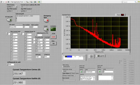
Concerning the spectral noise acquisition, the programmed LabVIEW interface allows to set several bias current values and several frequency ranges, with different averaging numbers for each one (see Fig. 1.3).
9
Figure 1.3 Control panel of the LabVIEW program dedicated to the noise spectral density
acquisition. Several frequency ranges, numbers of averages and bias current value can be set.
The program acquires two different temperature values, too: one from the GaAlAs thermometer, that is the cold finger temperature, the other value coming from the Cernox thermometer, attached to the sample holder.
The investigated samples have been contacted with the four-point, or Kelvin, probe method, that is the most common way to measure the resistance of a conducting material. This technique consists of two current carrying probes (the two outer contacts) and two voltage measuring probes (the two inner contacts). This arrangement eliminates measurement errors due to the probe resistance, and the contact resistance between each metal probe and the specimen material. More in details, the contact resistance refers to the contribution to the total resistance of a material which comes from the electrical leads and connections, as opposed to the intrinsic resistance which is an inherent property, independent of the measurement method. In the simple two-probe method, the measurement current causes a potential drop across both the test leads and the contacts so that the introduced parasitic resistance cannot be separated from the resistance of the device under test.
11
CHAPTER 2
N o i s e p r o p e r t i e s a n d t r a n s p o r t i n a g i n g
-i n d u c e d d e g r a d e d -i r o n - b a s e d
s u p e r co n d u c t o r s
Iron-based superconductors constitute a relevant discovery in the field of condensed matter physics. At the core of this family of compounds, iron-chalcogenides are considered ideal systems to better understand the transport and superconducting mechanisms, thanks to their simple chemical and crystallographic structure. In addition, a renovated interest on these materials has been registered, due to the recent observation of a superconducting transition above 100 K in FeSe films grown on SrTiO3 substrates [2].
The nature of superconductivity in iron-chalcogenides is still unclear, so that the study of the charge transport by means of noise spectroscopy could improve the knowledge about iron-based superconductors behavior. For this purpose, thermal and voltage activated excess 1/f noise has been associated to nonlinear conductivity fluctuations in Fe(Se,Te) thin films [3] previously.
Iron-based superconductors are prone to degradation when exposed to unprotected environmental conditions, with a very likely vanish of their superconductive properties. The understanding of aging effects is of interest in view of practical applications. In this respect, voltage-noise and electric transport measurements have been carried out on FeSe and FeSe0.5Te0.5 thin films, just
after fabrication and after long aging in protected environment. The uncontaminated films exhibit a superconducting transition at temperatures ranging from 9 to 12 K for FeSe and at 17 K for FeSe0.5Te0.5, and an overall
metallic behavior above Tc. Preserving the samples for several months in
low-humidity and low-pressure conditions, the FeSe0.5Te0.5 films does not show
evident modification of the electrical conduction mechanisms. Conversely, the superconductive transition is no longer present in the FeSe films, at least for temperatures above 8 K, and an overall larger resistivity is observed, with a characteristic upturn at low temperatures (T < Tmin ≈ 50 K).
2.1 Materials and methods
The investigated films were prepared at the Department of Basic Science, University of Tokyo (Japan) by a pulsed KrF laser deposition. The targets were made of polycrystalline pellets of FeSe and of FeSe0.5Te0.5, while commercial
single crystals of CaF2 (100) were used as substrates [4]. The optimal deposition
parameters, that is substrate temperature, back pressure, and laser beam repetition rate were: 7 K, 10−6 Torr, and 10 Hz, for FeSe; 7 K, 10−7 Torr and 20 Hz
for FeSe0.5Te0.5. The film thickness, ranging from 15 to 148 nm, was measured
using a Dektak 6-M stylus profiler. Four-circle X-ray diffraction (XRD) with Cu Kα radiation at room temperature was used to identify the crystal structure, indicating a good c axis film orientation [4].
The samples were patterned in an eight-terminal shape, by means of a metal mask, in order to obtain well defined geometries (see Fig. 2.1). Two equivalent types of electric contacts were used: wire bonding with silver paste, and mechanically pressed indium pads using a custom-made sample holder (see Fig. 2.1 for details).
Figure 2.1 Wire bonding contacted FeSe sample (left panel) and contacted FeSe0.5Te0.5 sample by
mechanically pressed indium pads on custom-made sample holder (right panel).
The latter was designed by the author with a PCB-CAD software, then manufactured on aluminium-ims (insulated metal substrate) which provides an optimal thermal conduction.
All the measurement were carried out by using the experimental setup described in the chapter 1.
2.2 DC electrical transport properties
Resistance versus temperature data has been measured in current-pulsed mode by biasing the samples with a current of 50 μA. The graphs depicting the resistance trends are shown in Fig. 2.2.
13
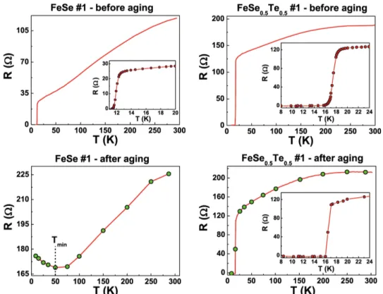
Figure 2.2 Temperature dependence of the sample resistance R of FeSe and FeSe0.5Te0.5 (left and
right panels, respectively), before and after aging (upper and lower panels, respectively). Green circles represent the temperatures, at which noise measurements have been performed.
Just after fabrication, the investigated samples show a superconducting transition, defined as 50% of normal state resistance, at a temperature Tc = 12.0
K for FeSe and Tc = 17.5 K for FeSe0.5Te0.5. After aging for several months in
protected atmosphere, the two Fe-based films are measured again and show a different behavior. As visible in the lower panels of Fig. 2.2, the FeSe0.5Te0.5 film
has preserved its transport properties with slight modification. A little increase of resistivity and a small decrease of the critical temperature from 17.5 K to 16 K are observed. Conversely, the FeSe sample does not show the pristine superconducting transition (at least for temperatures above 8 K), and the lowest explored temperature range exhibits an overall larger resistivity with a characteristic upturn at T < Tmin ≈ 50K. At a first glance, these experimental
findings suggest that the Te substitution into Se sites contribute to enhance Tc
2.3 Noise spectral density measurements
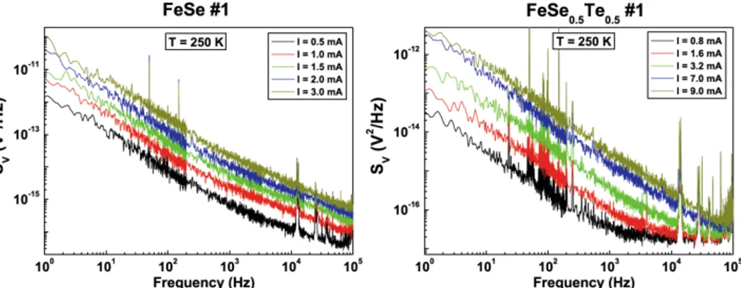
In order to obtain a more clear picture of the conduction properties, a detailed electric noise characterization of the samples has been performed for several bias currents and temperatures. Both of them, before and after aging, exhibit the same frequency dependence of the voltage-spectral density Sv. In
particular, in the range from few Hz to 105 Hz, the noise amplitude is
characterized by a 1/f behavior, followed by a constant value at higher frequencies, due to the instrumentation electronic readout and to the sample Johnson noise contributions. Captured spectral traces are shown in Fig. 2.3 at a fixed temperature of 250 K, for the FeSe (left panel) and the FeSe0.5Te0.5 (right
panel) thin films.
Figure 2.3 Frequency dependence of the voltage-spectral density Sv, acquired at a reference
temperature of 250 K and for different bias current values, of FeSe and FeSe0.5Te0.5 samples (left
and right panels, respectively).
The experimental voltage-spectral densities suggest, therefore, the use of the Hooge relation [1], ( ) 0 ( )
( )
( , , )
T V TK T
S f I T
I
C
f
η γ=
+
(2.1)where, K0 is temperature-dependent noise amplitude, γ and η are the
temperature-dependent frequency and current exponents, respectively, and C is the white noise contribution.
In this contest, it could be of help to evaluate the best fitting values for the parameters of Eq. (2.1). They have been calculated and reported in Fig. 2.4.
15
Figure 2.4 Temperature dependence of the fitting noise parameters: amplitude K0 (left y-axis),
frequency slope γ and current slope η (right y-axis). The data for FeSe and FeSe0.5Te0.5 samples,
after aging, are shown in the left and right panels, respectively.
The value of γ ranges between 0.8 and 1.2 for all the investigated temperatures and samples after aging. This clearly indicates that the dominant noise component is of 1/f-type [1]. A monotonic increase of K0 , with the
temperature, is observed for the FeSe0.5Te0.5 system while FeSe aged films show
an evident change of the noise properties below the crossover temperature Tmin.
The FeSe0.5Te0.5 compound is characterized by an electric field threshold E0 ,
above which a nonlinear excess noise is activated as proved by the parameter η, displayed in the right panel of Fig. 2.4 as blue triangles, whose value exceeds 2 at temperatures higher than 100 K. This behavior is not observed in the low-temperature region, where standard resistance fluctuations are the noise source, and it has been attributed to the presence of a structural transition near 100 K [5].
2.3.1 Weak-localization effects
The induced degradation of FeSe thin films produces an increase in the resistivity below Tmin, as clearly showed in Fig. 2.2. This characteristic feature,
already reported in scientific literature, is the sign of weak-localization (WL) effects. It has been demonstrated that nonequilibrium universal conductance fluctuations occur in the WL regime causing the linear bias current dependence of the 1/f noise component [6]. A further proof is given by the temperature dependence of η, as shown in Fig. 2.4 (left panel).
To gain a better picture of the phenomena, It may be worth investigating the nature of these quantum interference effects by analyzing the resistance values near Tmin. The R(T) curve could be described by using a 2D WL model or a 3D WL
Figure 2.5 The low-temperature resistance of a typical degraded FeSe sample, is reproduced in
terms of a 2D WL model (red curve) and of a 3D WL model (green curve). The relevant statistical parameters and the best fitting values of the characteristic index p are reported in the inset.
The distinctive parameter is the index p, which estimates are 3/2, 2, and 3, depending on whether the inelastic scattering rate is determined by Coulomb interactions in the dirty limit, in the clean limit, or by electron-phonon scattering [7]. Therefore, taking a look at the inset of the Fig. 2.5, the 3D WL model only results to be consistent by a physical point of view: It is characterized by an index
p close to 2, by the highest coefficient of determination r2 and by the lowest
reduced χ2. The index p value suggests that Coulomb interactions in the clean
limit determine the inelastic scattering rate.
To sum up, aging-induced degradation involve different effects in FeSe and FeSe0.5Te0.5 samples. While the presence of Te seems to enhance Tc , and to
stabilize the compound, completely different dc and ac behaviors are found in pristine and aged FeSe thin films. In particular, the superconducting transition vanishes with sample degradation, and an upturn of the resistivity is observed below a crossover temperature of 50 K. The 1/f noise component shows an unusual bias current dependence in the low-temperature region, with a clear shift from a quadratic to a linear trend. This experimental evidence corresponds to the occurrence of nonequilibrium universal conductance fluctuations, and is the distinctive feature of weak-localization effects. The weak-localization theory proves the presence of aging-induced scattering centers in the FeSe compound by modeling the low-temperature resistance. The 3D WL model only provides coherent physical parameters from which information on the dimensionality and the type of scattering mechanism can be gathered.
17
Author contribution The author performed the R(T) and voltage
noise-measurements of all devices. The author designed the custom-made sample holder by means of a CAD software.
19
CHAPTER 3
N o i s e p r o p e r t i e s a n d t r a n s p o r t i n
d i f f e r e n t p o l y m e r / c a r b o n n a n o t u b e
c o m p o s i t e s
The importance of Carbon nanotubes (CNTs) has grown over time, having novel properties that make them potentially useful in a wide variety of applications in nanotechnology, electronics, optics and other fields of materials science. A carbon nanotube is a tube-shaped material, made of carbon, with a diameter on the nanometer scale. CNTs exhibit extraordinary stiffness and unique electrical properties, and are efficient conductors of heat.
For the realization of CNT based transistors, single-wall carbon nanotubes (SWCNTs) are the best solution. Recently thin film transistors (TFTs) made from networks of semiconductor-enriched SWCNTs have reached performances that outperform the commercial state-of-the-art thin film transistor technologies [8]. Conversely, Multi-wall carbon nanotubes (MWCNTs) generally have metallic behavior that play an important role as transparent conductive contacts for RF-shielding, for solar cells and as sensors and actuators.
Electrical noise is typically a limiting factor for the functionality of electronic devices and sensors. While many studies inspect the noise behavior of devices prepared with SWCNTs, fewer reports on noise characteristics of MWCNT composites exist. In particular, it is worth investigating the interaction between multi-wall CNTs and different type of polymer or epoxy matrix, and the influence over their mechanical and electrical properties.
In this chapter, dc transport measurements and voltage noise analysis on different polymer/carbon nanotubes composites are presented. The transport property measurements show that a random tunnel junctions resistive networks model well describes all the compounds under test. In particular, with increasing the temperature, a crossover from a two-level tunneling mechanism to resistance fluctuations percolative paths induced has also been observed. Moreover, this 1/f noise trend seems to be a general feature of the investigated highly conductive samples, going beyond the type of polymer matrix and nanotubes concentration.
3.1 Materials and methods
The investigated composites were prepared by mixing CNTs in different polymeric matrices. MWCNTs were synthesized by chemical vapor deposition at CSIRO (Commonwealth Scientific and Industrial Research Organization, Australia) and dispersed in two polyethylene bases, with an average molecular weight of
≈60000 g/mol and a polydispersity of 5.8 (High-density polyethylene HDPE0390 from Qenos) and ≈115000 g/mol and a polydispersity of 7.6 (Low-density polyethylene LDPE from Scientific Polymer Products), respectively, with two MWCNT concentrations (5 and 7 wt%). In addition, MWCNTs synthesized by catalytic carbon vapor deposition process (Nanocyl S.A.) were incorporated in a diglycidil-ether bisphenol-A (DGEBA) epoxy resin, with a concentration of 0.5 wt%. Basically, polymeric matrix compound is considered as insulating material because of its high electrical resistivity (1010-1015 Ωm). Injecting conductive
material into the insulating matrix can lead to an overall conductive compound, strongly depending on the volume fraction of the conductive phase. In particular, below a threshold volume fraction, the conductibility of the composite dramatically increases by several orders of magnitude due to percolation. In conclusion, CNTs add several features to the composites: at low loading, CNTs act as a conductive additive, due to their low percolation thresholds (between 1 and 2.5 wt% for HDPE and LDPE, and lower than 0.1 wt% for epoxy), while uniformly dispersed in higher percentage, enhance its mechanical properties [9]. The detailed information reported in [10] and [11] indicate that all the used polymer/carbon nanotubes compounds are suitable for sensor and conductor applications, due to their high conductivity values. This behavior of the composites seems to be not influenced by the presence of a bundle organization which, however, has been observed through a scanning electron microscopy analysis.
The experimental setup provides both two- and four-probe connections to the samples through evaporated gold contact pads (25-nm-thick, 5-mm-wide and about 1-mm-distant). All the measurement were carried out by using the experimental setup described in the chapter 1. Possible effects of spurious external noise sources were eliminated by resorting to proper techniques, as described in [12].
3.2 DC electrical transport properties
The temperature dependence of the resistance R for the five investigated MWCNT composites is shown in Fig. 3.1. The clear monotonic decrease with increasing temperature is best interpreted by Sheng model [13]. Other possible models, such as variable range hopping and Luttinger liquid models reproduce the experimental data, but does not give a low reduced χ2 and the high
21
Figure 3.1 Temperature dependence of the resistance R for the five different types of investigated
MWCNT compounds. The dashed and solid lines are the best fitting curves with Eqs. (3.1) and (3.2)
In the case of carbon nanotubes compounds [14], a fluctuation-induced tunneling conduction between conducting regions (the MWCNTs) and small insulating barriers (the matrix) is modeled through the following expression
1 0 0
( )
T
R T
R exp
T T
=
+
(3.1)where R0 is a preexponential factor, and T0 and T1 are two characteristic
temperatures of the systems under test [13]. The best fit curves by using Eq. (3.1) are shown in Fig. 3.1 as dashed lines, revealing a good agreement with the data points along the whole temperature range and for all the samples. The estimation of T1, reported in Table 3.1 together with all the other fitting
parameters, allows the evaluation of the minimum energy (Δϵb≃kBT1) necessary
to cross the insulating barriers formed among the nanotube aggregates [14]. These values in Table 3.1 are similar to those observed for various carbonaceous materials, analyzed in terms of the Sheng model.
Table 3.1 Temperature dependence of the resistance R for the five different types of investigated
MWCNT compounds. The dashed and solid lines are the best fitting curves with Eqs. (3.1) and (3.2)
In the high-temperature region, a different conduction mechanism takes place due to the thermal activation over the potential barrier [15].The temperature dependence of the resistance is described by
2 1 1 0
( )
(1
)
(
c)
A cT T
R T
R exp
T T T
=
−
+
(3.2)Where R1 is a preexponential factor, ϵA is the dimensionless applied electric field,
and Tc is a crossover temperature above which the fluctuation-induced tunneling
and thermal activation contributions are indistinguishable [13]. The solid lines shown in Fig. 3.1 are the best fitting curves with Eq. (3.2), and obtained with the values of Tc reported in Table 3.1. These crossover temperatures, associated to
the energy distribution of the tunnel barriers, give an immediate morphological information on the interaction between the polymer matrix and the carbonaceous filler. It is worth to note that, in Eq. (3.2) the dimensionless applied electric field ϵA only gives, as a first approximation, a negligible
contribution to the evaluation performed. However, the dc analysis, alone, is not able to identify the different transport mechanisms of charge carriers at high temperatures. In this context, noise spectroscopy is the right tool for a deeper insight.
3.3 Noise spectral density measurements
The spectral density of voltage fluctuations SV is the physical quantity to
examine if we want to deal with electric noise. The frequency dependence of SV
is shown in Fig. (3.2) for the different types of MWCNT compounds at the reference temperature of 300 K. All the spectra can be regarded as superposition of two main components: the first determines a 1/f dependence in the low-frequency region and the second, characterized by a constant spectrum at higher frequencies, is due to the Johnson noise 4kBTR added to the background
23
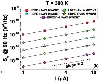
Figure 3.2 Spectral traces of all the investigated MWCNT composites at a reference temperature
of 300 K and bias current of 4 μA.
In order to find out the dynamics of fluctuations and the conduction mechanisms, it is useful to study the 1/f contribution versus the applied bias current. This dependence is shown in Fig. 3.3, revealing a quadratic behavior for all the samples under test and, as a consequence, resistance fluctuations as the dominant noise source.
Figure 3.3 Quadratic bias dependence of the voltage-spectral density for all the investigated
In this framework, the noise level of Ohmic compounds can be expressed by using the Hooge relationship as [1]
2 2 1 V H s f S Noise Level R I n
α
= = Ω (3.3)where αH is the dimensionless Hooge material-dependent constant, n the
carrier density, and Ωs the sample volume.
3.4 Fluctuation induced tunneling model applied to noise
processes
The best way [15],[16],[17] to model the noise level in this kind of disordered systems is given by 2 0 c w c AT R T T Noise Level S R T T − < = > (3.4)
where A is a proportionality factor, S0 is the amplitude of resistance
fluctuations, w represents the critical indexes for lattice percolation, and Tc is the
crossover temperature between the fluctuation-induced tunneling and thermal activation regimes. The parameters A and S0, alone, are not sufficient to extract
the intrinsic noise of the material, which is further dependent on the sample temperature, resistance, and volume. In details, below Tc, two-level tunneling
system (TLTS) fluctuations dominate, while above Tc thermal activation must be
considered, as a consequence of the percolation model [16]. It must be stressed that the two-level tunneling mechanism has successfully been used for the interpretation of the noise in individual nanotube samples [18], and also for HDPE compounds below the crossover temperature [7]. The experimental noise level, compared with the theoretical formulation given by Eq. (3.4), is shown in Fig. 3.4.
25
Figure 3.4 Temperature dependence of the Noise Level of all the investigated samples. The best
fitting curves obtained by using a two-level tunneling system model [see Eq. (3.4), T<Tc] and a
percolative noise mechanism [see Eq. (3.4), T>Tc] are shown as dashed and solid lines,
respectively. The transition between these two regimes occurs at the crossover temperature, estimated from the dc analysis. The percolative model of HDPE +5wt% MWCNT composite is not shown, being out from the examined temperature range (Tc> 300 K).
Below Tc, the good agreement of TLTS model (dashed lines) with the data points
is clear. On the other hand, the percolative fluctuation process (solid lines) prevails in the temperature region above Tc. Such a behavior is independent of
the polymer matrix chosen for the device fabrication. By comparing Eq. (3.4) with Eq. (3.3), it is possible to extract the normalized Hooge parameter as
2 0 S c w c S H A T R T T n S R T T
α
− < = > Ω Ω (3.5)More in details, the exponent w assumes values of 1 for epoxy, 1.01 for LDPE, and 1.06 for HDPE. These are very close to the value predicted by the classical percolation theory in the case of three-dimensional systems [19]
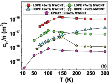
The quantity αH/n is evaluated by means of the Eq. (3.5), where Ωs is the
volume of the entire composite, that is the polymeric matrix and the conductive nanotubes. The results are shown in Fig. 3.5.
Figure 3.5 Temperature dependence of the normalized Hooge parameters computed with Eq.
(3.5).
The epoxy based composite seems to be the most promising in high sensitivity applications, due to its lowest noise level in the whole investigated temperature range.
Author contribution The author performed the R(T) and voltage
noise-measurements of all compounds. The author contributed to the theoretical interpretation of the experimental findings.
27
CHAPTER 4
N o i s e p r o p e r t i e s a n d t r a n s p o r t i n
c r y s t a l l i n e s i l i c o n - b a s e d s o l a r c e l l s
Crystalline silicon photovoltaic (PV) cells are the most common solar cells used in commercially available solar panels, representing more than 90% of world PV cell market sales in 2012. Crystalline silicon PV cells have laboratory energy conversion efficiencies over 25% for single-crystal cells and over 20% for multicrystalline cells. However, industrially produced solar modules currently achieve efficiencies around 20% under standard test conditions.
It is well known that quality and efficiency of Crystalline silicon PV cells are related to several electronic parameters of the defect states.
This chapter shows that low-frequency noise spectroscopy is a powerful and unconventional tool for the investigation of the properties of the defect states in silicon-based solar cells. Around 1970, Van der Ziel [20] and Hsu [21] related the
1/f-type noise in the metal-oxide-semiconductor system and in p-n junctions to
the fluctuation of the defect state population. Twenty years later, Jones [22] and Chobola [23] proposed low-frequency electric noise analysis to estimate quality of solar cells. Semiconductors often exhibit a 1/f-type noise spectrum. Semi-empirical models have been formulated to correlate the current noise to mobility fluctuations [24], to the number fluctuation of free charge carriers within the space charge region [25], or to the semiconductor surface.
A theoretical model, combining trapping/detrapping and recombination mechanisms, is formulated to shed light on the origin of random current fluctuations in silicon-based solar cells. The comparison between dark and photo-induced noise allows the determination of important electronic parameters of the defect states. A detailed analysis of the electric noise, in several conditions of temperatures and for different illumination levels, is reported for crystalline silicon-based solar cells, in the pristine form and after artificial degradation with high energy protons. The evolution of the dominating defect properties is studied through noise spectroscopy.
Findings suggest that the formation of the defects, activated under illumination or charge carrier injection, is related to long-term degradation of the solar cells. Moreover, noise analysis provides interesting information on radiation damage, and can be used for a detailed temperature-dependent electrical characterization of the charge carrier capture/emission and recombination kinetics. This aspect represents an advantage of the fluctuation spectroscopic technique, which gives the possibility to directly evaluate the cell health state.
4.1 Materials and methods
The investigated solar cells, type “SC2140-Z8-24” were manufactured by SOLARTEC (Radhoštěm, Czech Republic). The useful area A of the photovoltaic devices was 1 cm2 with a wafer thickness d of 320 μm. The starting efficiency of
pristine samples was 15% under AM 1.5 G conditions, with a short-circuit current
Isc = 37.45 mA, open-circuit voltage Voc = 581 mV, and fill factor FF = 68.96%.
Degradation effects were artificially induced on the devices with proton irradiation at the Helmholtz-Zentrum Berlin für Materialien und Energie (Germany), with a proton energy of 65 MeV in air. A homogeneous defect distribution, with this energy value, was verified by using a SRIM (Stopping and Range of Ions in Matter) code. Additional details on the performed analysis can be found in [26]. The samples were irradiated with three different proton fluences: 2 × 10¹¹ protons/cm2, 1 × 10¹² protons/cm2, and 5 × 10¹² protons/cm2.
All the measurements were carried out by varying the temperature from 280 to 340 K with a thermoelectric cooler, and by stabilizing it with a computer-controlled PID loop to better than 0.1 K. The cool white Light Emitting Diode (LED) “KLC8 Edixeon K series”, from Edison Opto, was used as light source. The choice of the LED as light source ensured a low-noise source, allowing to discriminate intrinsic photo-induced mechanisms from extrinsic ones, potentially related to the complex electronics of the solar simulator. The setup for the electrical transport and noise characterizations was arranged in order to minimize the presence of spurious components in the measured spectral traces. External noise contributions, such as light source emission noise, light source bias circuit noise were also evaluated and found to be negligible as reported in the Supplementary information of [27].
4.2 Noise model of solar cells
Bias voltage, photogeneration processes and diode geometry greatly affect fluctuations phenomena in p-n junctions. When defect states are present, the trapping and recombination mechanism of the charge carriers gives rise to current fluctuations, which represent the main noise source [28]. The amplitude of the random current fluctuations Var [I] is, therefore, related to the occupation probability ftrap of the traps. The recombination pathways from the conduction
band to the valence band generate a decrease of the minority charge carriers stored in the base material, and this effect also influences Var [I]. The contribution of the traps can be modeled by the means of two energy levels, which act as trapping (ET) and recombination (ESRH) centers. These centers,
located above the intrinsic Fermi level Ei (see Fig. 4.1 (a)) are responsible for the
transitions between the defect states and the conduction EC and valence EV
29
are able to capture and emit electrons from the conduction band and the ESRH
states work as Shockley-Read-Hall (SRH) type recombination centers with an associated lifetime τSRH [29].
Figure 4.1 (a) Energy-band diagram of the silicon showing carrier recombination and trapping
processes. (b) ac electrical equivalent circuit of the solar cell. (c) Equivalent circuit including noise
sources. (d) Simplified version.
The fluctuating traps with energy level ET can be modeled by a series RC
circuit in parallel to Cμ [30], as shown in Fig. 4.1 (b) where the differential
resistance RD and the capacitance Cμ represent the contribution of the minority
charge carriers into the base material. Moreover the cell shunt Rsh and series RS
resistances take into account the recombination loss and ohmic series resistance respectively. Usually Rsh»RD and the recombination phenomena, associated to
the defect states, can be well described by the time constant τeff = RDCμ. The
density of empty traps into the base material can be modeled by a capacitance contribution Ctrap, which is related to the variation of ftrap with respect to the
quasi-Fermi level under nonequilibrium condition (charge carrier injection). On the other hand, the resistance Rtrap represents the kinetic factor of the traps [30],
which characteristic trapping/detrapping time is τtrap = Rtrap Ctrap. Below the
frequency (2πτtrap)−1, the capacitive contribution of the fluctuating trap states is
important so that noise spectroscopy is able to follow the charge carrier transfer from the conduction band to empty traps and viceversa (see Fig. 4.1 (c)). This mechanism leads to fluctuations in the number of charge carriers and contributes, therefore, to a current fluctuation that can be measured by the external contacts. The effect of these traps can be modeled as a current-noise source in, which represents the charge carriers transfer between Ctrap and Cμ (see
Fig. 4.1 (d)). The solar cell equivalent noise circuit can be assumed as simply composed by the parallel connection of Cμ, RD, and in, as shown in Fig. 4.1 (d).
The noise is generated by the variation in the number of carriers, that are typically present in the cell, due to the dc bias or light absorption. A characteristic 1/f frequency spectrum is observed, with the presence of a cut-off frequency given by fx = (2πτeff)−1 [31].
In this context, the amplitude Var [I] of the 1/f noise component can be defined as the sum of a dark (Var [Idark]) and a photo-induced (Var [Iph])
contribution. Under dark condition and on forward biasing of the solar cell, the
Var [Idark] value is influenced by the emission rates en,p and volumetric capture
coefficients per unit time cn,p for the electron and hole traps [29]. When the cell
is illuminated, these capture coefficients, the emission rates and the density of filled traps change. Consequently, the process of carrier photogeneration increases the trap filling up to a saturation point, meaning that all traps have been activated from the noise point of view. In this condition, the Var [Iph]
contribution is dominant, being larger than the dark background noise. The photogenerated current can be expressed as [32]
ph eff n q I Ad
τ
= (4.1)where q is the elementary charge, n is the average excess carrier density, and A and d are the sample area and thickness, respectively. By taking SRH statistics into account, the fraction nT of the filled fluctuating traps is [32]
T n T n n N e n e c n = + (4.2)
The fraction of the filled recombination centers is [32]
SRH p A SRH n p A
N c N
n
c n c N
=
+
(4.3)31
where NA is the base doping concentration. In Eq. (4.1) it is worth noting that
the only fluctuating term is related to n, therefore, under the assumption of a binomial probability distribution, Var [Iph] can be expressed as [1]
2
{ [ ] [ ]}
ph T SRH
eff
q
Var I =
τ
Var Adn +Var Adn (4.4)
Substituting Eq. (4.2) and (4.3) into Eq. (4.4) follows
2 2 2
[ ]
1
n1
n n SRH n ph T eff A p n A p nc
n
e
N
c
q
n
Var I
Ad N
N c
c
n
n
e
N
c
c
τ
=
+
+
+
(4.5)where cn /cp = k is the symmetric ratio [33].
Moreover 0ght n eff n li q e I Ad c
τ
= (4.6) and A A eff N q I Ad kτ
= (4.7)Eq. (4.5) can be rewritten as
1 2 2 2 0 1 1 ph ph ph ph ph light A I I Var I A A I I I I = + + + (4.8) where 1 T n eff n c q A N e
τ
= and 2 SRH eff A q k A N Nτ
= (4.9)represent the amplitudes of the current fluctuations related to the trapping and recombination mechanisms, respectively. When the noise level is almost
saturated the threshold current I0light happens, and IA takes into account the
influence of the recombination centers.
4.3 Noise spectral density measurements
The effectiveness of the proposed noise model has been verified by measuring the same type of Si-based solar cells, in two different form: pristine and proton irradiated to gain an increasing numbers of traps.
Pristine Si-based solar cells. The first step is the acquisition of the
voltage-spectral density SV generated by the device in various operation conditions. In
Fig. 4.2, the Voltage-spectral density of pristine solar cells is shown at a temperature of 300 K and for different bias points, corresponding to several differential resistance values. A large 1/f component is evident, followed by a constant amplitude spectrum at higher frequencies, both in dark, see Fig. 4.2 (a), and under illumination, see Fig. 4.2 (b). The measured noise can be expressed as [1]
C
VK
S
f
γ=
+
(4.10)Where K is the voltage-noise amplitude, γ = (1.18 ± 0.02) is the frequency exponent, and C = 1.04 × 10⁻¹⁷ V2/Hz is a negligible frequency-independent noise
component, due to the readout electronics.
Figure 4.2 (a) Frequency dependence of Sv at 300 K and for increasing values of the differential
resistance RD in dark condition. (b) Frequency dependence of Sv at 300 K and for increasing values
33
After a careful examination of the 1/f noise, interesting information on the conduction mechanisms and the dynamics of fluctuations can be extracted. The variance of the voltage is given by [1]
( ) ( ) max min 1 1 max min
[ ]
(1 )
f V ff
f
Var V
=
df S
=
K
−γ−
γ
−γ−
∫
(4.11)where the frequency interval [fmin, fmax] = [1, 100000] Hz is the experimental
bandwidth, and γ ≠ 1. The Var [V] exhibits a quadratic dependence on RD not
depending on illumination and temperature conditions, as shown in Fig. 4.3 (a) for the sample temperature of 300 K.
This behavior indicates that current fluctuations are the dominant noise source in the photovoltaic system. The amplitude is given by [1]
2 [ ] [ ] D Var V Var I R = (4.12)
and is independent on RD, as clearly evident in Fig. 4.3 (b).
Figure 4.3 (a) Dependence of the 1/f voltage noise amplitude on the differential resistance and on
photocurrent at 300 K. (b) Dependence of the current fluctuations amplitude on the differential
resistance under illumination at 18 mW/cm2 (circles) and under dark condition (squares) at 300 K.
The photo-induced fluctuations amplitude has been analyzed at a fixed bias condition of RD = 10 Ω, and is shown as current noise in Fig. 4.4 at four different
Figure 4.4 Photocurrent dependence of the current fluctuations amplitude at 280 K (a) , 300 K (b) ,
320 K (c) and 340 K (d). The blue solid lines represent the best fitting curves using Eq. (4.8), while
black dots represent noise level in dark condition.
Under the low-level injection operating conditions of most silicon solar cells [34], the SRH recombination is the dominant mechanism influencing the minority charge carrier lifetime. In this framework, it can be assumed that τeff = τSRH .
Furthermore, 0 0 1 light SRH n A I I τ τ + = (4.13)
where τn0=(cnNSRH)-1 and I0light /I . It follows that τA 1 SRH ≈ τn0 but τn0 is
weakly temperature-dependent below 340 K [33], so the value of τeff can be
assumed constant [26]. It is worth noting that the effective lifetime can be directly estimated from the noise spectra, when the cut-off frequency occurs within the experimental frequency bandwidth [31]. By using Eq. (4.6), Eq. (4.7) and Eq. (4.9) it is possible to compute the most important defect states parameters including the number of the fluctuating traps NT .
35
The temperature dependence of NT is reported in Fig. 4.5 (left axis), and it
does not change within the experimental errors in the whole analyzed temperature range.
Figure 4.5 The fluctuating trap density NT is shown as a function of temperature on the left y-axis
(yellow squares), while the energy depth of the traps EC − ET is shown on the right y-axis (green circles). For a better readability, the right scale only reports the upper half EC − Ei of the bandgap.
It must be stressed that, the average value of NT = (8.4 ± 0.1) × 1015 cm−3 is
close to the doping concentration NA ≈ 9 × 1015 cm-3, and this is consistent with
the formation of unstable boron-oxygen defects. A further validation comes from the energy depth of the traps below the conduction band, that can be estimated from C 0 ln c T B light eff N q E E k T Ad I
τ
− = (4.14)where kB is the Boltzmann constant, T the temperature, and NC the effective
density of states in the conduction band [32]. The temperature dependence of the trap energy is shown in Fig. 4.5 (right axis), from which an average value of
EC−ET = (0.41 ± 0.04) eV can be evaluated. Once again, the estimations of EC−ET
and of the symmetric ratio k = (30.9 ± 0.8) at 300 K are consistent for a metastable boron-oxygen defect in Czochralski grown silicon, as reported in literature where k = 6.2 − 33.6 and EC − ET = 0.39 − 0.46 eV [33].
Proton irradiated Si-based solar cells. The frequency dependence of SV found
for pristine devices is also observed for all the silicon solar cells irradiated with different proton fluences. In Fig. 4.6 (a), the presence of a 1/f noise component followed by a constant amplitude spectrum at higher frequencies is clear. The current-noise amplitude Var [I] can be computed from Eq. (4.12) and does not depend on RD, (see Fig. 4.6 (b)) due to the fact that the 1/f contribution is
characterized by a quadratic dependence on the differential resistance RD. Again,
the overall trend is completely independent on proton irradiation, light intensity and temperature, thus indicating current fluctuations as the dominant noise source [1].
Figure 4.6 (a) Frequency dependence of Sv at 300 K and for increasing values of the differential
resistance RD for a proton irradiated silicon solar cell with fluence of 5 x 10¹² protons/cm2. (b)
Frequency dependence of Sv at 300 K and for increasing values of the differential resistance RD
under illumination.
By comparing the photocurrent dependence with that of pristine devices it is found to be similar. Therefore the theoretical model of Eq. (4.8) can be applied to the artificially degraded silicon solar cells too. The results are depicted in Fig. 4.7.
37
Figure 4.7 Dependence of the current fluctuations amplitude on the photocurrent for pristine and
irradiated devices and for temperature ranging from 280 K to 320K. The experimental data points (red) and the best fitting curves (blue solid lines) descend from Eq. (4.8). The arrows show the increasing proton fluences.
The dependence on irradiation level of the defect states parameters, extracted from the noise analysis, allows to evaluate the effect of radiation exposure, and the corresponding damage of the cells, which is also associated to a decrease of the energy conversion efficiency [26]. In Fig. 4.8 (left axis), is shown the density NT of active traps contributing significantly to the noise signal,
that increases with the fluence of proton irradiation. This occurrence gives a direct indication of the presence of additional degradation processes in the photovoltaic device, confirmed by the increase of the dark background noise amplitude. It proves that the defects induced by damaging the samples have the same role in the fluctuation mechanisms both in dark and under illumination. At the same time, a weak decrease of the trap energy depth is displayed in Fig. 4.8 (right axis).
Figure 4.8 Proton fluence dependence of the fluctuating trap density NT (left y-axis and yellow
squares), and of the energy depth of the traps EC − ET (right y-axis and green circles), at 300 K.
The observed effects on NT and on EC−ET are consistent with the reported
long wavelength decrease of the external quantum efficiency (EQE), due to the increase of recombination centers density caused by proton irradiation [26]. Moreover, in Fig. 4.8, it is worth noting the abrupt change after the first dose of radiation. This finding suggests that the major disturbance of the structure, leading to a noise enhancement, occurs at the beginning of radiation exposure. The values reported in Table 4.1 support this experimental evidence. In particular, the simultaneous decrease of the main solar cell photoelectric parameters and the increase of trap density seem to be directly related to an overall reduction in the power conversion efficiency (PCE).
Table 4.1 Main parameters, at room temperature, of the Si-based solar cell for the evaluation of
the degradation induced by proton irradiation. Open-circuit voltage Voc, short-circuit current Isc,
and power conversion efficiency η are extracted from dc analysis, while total trap density NT is
extracted from noise measurements.
In conclusion, it has been shown that the proposed theoretical model is able to explain the nature of current fluctuations in solar cells and it has been verified
39
both on pristine and artificially degraded Si-based devices. In particular, a combination of trapping/detrapping processes and charge carrier recombination phenomena has been considered to explain the current fluctuation mechanisms. In pristine cells, the energetic position and the symmetric ratio are in good agreement with the values obtained by using alternative techniques, and well consistent with the boron-oxygen complex defect. On the other hand, in degraded devices, the total trap density increases with the fluence of proton irradiation and seems to be directly related to a decrease of the power conversion efficiency. All these findings prove that noise spectroscopy is a reliable tool for the electrical temperature-dependent characterization of electronic defects in photovoltaic devices too.
Author contribution The author contributed to the voltage
noise-measurements of all devices. The author contributed to the discussion of the results and the implications.