Università degli Studi di Ferrara
DOTTORATO DI RICERCA IN
"FISICA"
CICLO XXIVCOORDINATORE Prof. Filippo Frontera
A NUMERICAL APPROACH TO OHMIC LOSSES ASSESSMENT IN CONCENTRATING PHOTOVOLTAIC SYSTEMS
Settore Scientifico Disciplinare FIS/01
Dottorando Tutore
Dott. Pasquini Matteo Prof. Guidi Vincenzo
_______________________________ _____________________________
(firma) (firma)
v
ACKNOLEDGEMENTS
I would like to acknowledge my supervisors, Dr. Donato Vincenzi and Prof. Vincenzo Guidi, for providing me the guidance to carry through this research.
I am also grateful to Prof. Giuliano Martinelli for the trust he put in me three years ago, when I joined this research group.
I wish to express my sincere gratitude to Dr. Stefano Baricordi, for his precious advices in many situations.
I would like to thank my colleague Dr. Federico Gualdi; he shared with me an important part of our research activity. Our challenging discussions helped me a lot in gaining a deeper insight into our field of research.
I would also like to thank my referees, Dr. Gianlucà Timò and Prof. Alfonso Damiano. Finally, I must acknowledge my parents for their constant support.
This research activity has been funded by EU project Apollon (grant agreement n. 213514), FIRB national project Fotoenergia (RBIP06N57B), Sardinia regional law 7/2007 (CUP F71J09000270002), STMicroelectronics and Angelantoni Industries.
vi
Table of Contents
1 Introduction to Photovoltaic (CPV) Systems ...1
1.1 Reflective Concentrators ...2
1.2 Refractive Concentrators ...4
1.3 Fresnel Lens...5
1.4 Secondary Optics for Fresnel Lenses ...8
1.5 Central Receiver Reflectors ...11
1.6 Optical Design of a Cassegrainian Concentrator ...11
1.7 Cassegrainian Concentrator System Featuring Spectral Splitting ...13
1.8 Introduction to Concentrator Solar Cells ...14
2 Ohmic Losses in Solar Cells ...22
2.1 Internal Resistance Problem ...22
2.2 I-V Curve Formation in Solar Cells with Distributed Parameters ...28
2.3 Experimental Measurement of the Distributed and Lumped Resistance Components ...37
2.4 Resistance of the Metallic Contact Grid ...41
2.5 Effective Distributed and Effective Series Resistances ...44
2.6 Conversion Efficiency of Solar Cell with Internal Ohmic Losses ...52
3 Physical Effects Arising in a Silicon Solar Cell Operating under Concentrated Sunlight ...57
3.1 High Doping Effects ...57
3.1.1 Many-Body Effects ... 57
3.1.2 Random Impurity Distribution ... 58
3.2 Effects of Heavy Doping on Minority Carrier Concentration ...69
3.3 Recombination in Heavily Doped Silicon ...63
3.4 Solar Cell Performances in The Presence of Heavy Doping Effects and High-Level Injection ...66
3.5 Temperature Effect ...70
4 A 2.5D Distributed Solar Cell Model ...72
vii
4.1.1 Resistor Values Calculation ...75
5 Concentrator Solar Cell Behaviour under Uneven Illumination Profiles ...79
5.1 Zemax Main Features ...79
5.2 Case Studies ...81
5.3 PV Device Model ...82
5.4 Simulation Results ...84
6 Analysis of non-Conventional Front Contact Patterns Impact on Concentrator Solar Cells Performances ...86
6.1 Basics of Fractals ...87
6.2 Implemented Contact Geometry ...88
6.3 Case Studies ...90
6.4 Simulation Results ...91
7 Analysis of Void Formation Effects in Concentrator Silicon Solar Cells Soldered to Metal Core Printed Circuit Board (MC-PCB) ...95
7.1 Preliminary Experimental Measurements ...96
7.2 Thermal Simulations ...97
7.3 Electrical Model ...98
7.4 Electrical Simulations ...99
A Appendix ...102
A.1 MATLAB Source Code ...102
A.1.1 MATLAB Script ...102
A.1.2 Function Correnti ...109
A.1.3 Function Crea_Maschera ...115
A.2 PSPICE Netlist ...115
A.3 Function Crea_Maschera ...125
viii
Table of Figures
Figure 1.1 The 350-kWp SOLARAS project power plant built and deployed in Saudi Arabia by Martin Marietta using Sandia
Labs technology [1]. ...2
Figure 1.2 ENTECH mid-concentration photovoltaic module design using arched linear Fresnel lens [2] ...2
Figure 1.3 Schematic representation of reflection ...3
Figure 1.4 Reflective concentration from a curved surface ...3
Figure 1.5 Refraction of a light ray passing through a transparent material ...4
1.6 Refraction of light rays passing through a plano-convex lens (left) and a Fresnel lens (right). ...4
Figure 1.7 Top view of a typical Fresnel lens...5
Figure 1.8 (A) A sketch of the cross section of a conventional lens and above a corresponding Fresnel lens with the same size and focal length. (B) The concentric segments of the Fresnel lens are sketched in a plan view. ...6
Figure 1.9 (A) A typical loss mechanism of a flat Fresnel lens are sketched. In practice, the active side of each facet refracts incoming light rays toward the focus. Ideally, the shape of a facet is hyperbolic; however, in practice, it is often approximated linearly. Typically, light rays are misguided at peaks and valleys of the facets, which cause a decrease of the optical efficiency. Furthermore, the groove wall of each facet is typically slightly tilted in order to provide a reliable de-molding during the manufacturing process. This also has a negative impact on the optical efficiency of the Fresnel lens. (B) A dome Fresnel lens is sketched. As a result of the bowed surface structure, the light rays are refracted at two surfaces. Thus, direct light rays can be refracted in a relative steep angle at comparable low reflection and aberration losses. Furthermore, when direct light is impinging perpendicularly on the dome Fresnel lens, the grooved side of the facets and the peaks does not impact the light rays. Consequently, these parts of the domed Fresnel lens do not decrease the optical efficiency . ...7
Figure 1.10 A profile of the measured intensity in the spot of a 40 × 40 mm2 Fresnel lens is shown. The measurement was carried out with monochromatic light at a setup developed at the Fraunhofer ISE [18] ...9
Figure 1.11 (A) The angular transmission of two test modules with six Fresnel lenses (40 × 40 mm2) and six solar cells (4.15 mm2) is shown. In principle, both modules have the same components, except for an additionally mounted reflective secondary optic on one of the modules. The short-circuit current of the modules was measured outdoors under a varying sun vector angle. (B) A photo of a test module equipped with reflective secondary elements is shown. ...9
Figure 1.12 A typical CPC and its section view ... 10
Figure 1.13 Modeling of focal point for 0° (a) and 1° (b) pointing error. At 0°, all the light strikes the cell; with no guide, a 1° pointing error moves nearly all the focused light fully off the cell; with the guide, all of the light is reflected back onto the cell active area. ... 12
Figure 1.14 Cross section through the center of the optics for an aplanatic Cassegrainian optical system with tertiary element light guide. The light guide greatly expands the tolerable pointing error ... 12
ix Figure 1.16 Dual-focus Cassegrainian PV module with dichroic secondary for use with separate multijunction solar cells ... 14 Figure 1.17 Tricroic Cassegrainian concentrator realized at the Physics Department of the University of Ferrara. Overall structure (top left), box containing the three receivers placed at the back side of the primary mirror (top right) and pictorial representation of the working principle (bottom) ... 15 Figure 1.18 The band energy diagram of a p-n junction under illumination: in the short-circuit regime (left), in the open-circuit regime (center) and connected to an external load resistance (right). ... 15 Figure 1.19 Illuminated I-V curve of a p-n junction in GaAs and I-V characteristics of load resistance Rl for different
magnitudes of Rl, 0.1 Ω (1), 1.026 Ω (2) and 10 Ω (3). ... 17
Figure 1.20 Dependences of the photocurrent density on the energy gap Eg, for the spectra AM 0 and AM 1.5D ... 20
Figure 1.21 Curve 1 – the energy spectrum AM 0 for non-concentrated sunlight; lines 2, 3 and 4 – plots of maximum monochromatic efficiency off an idealized solar cell for iph = 0.1; 1 and 10 A∙cm-2 respectively; sloped lines – spectral
dependences of conversion efficiency in the idealized solar cells based on In0.5Ga0.5P, GaAs and Ge, at iph = 1 A∙cm-2; curves
5, 6 and 7 show the portion of solar energy converted into electricity in the corresponding solar cells. ... 21 Figure 1.22 Maximum thermodynamic conversion efficiency of a solar cell made of a material with an energy gap Eg, where
T = 300 K. 1, 1’ – Ks = 1; 2, 2’ – Ks = 1000; 1, 2 – for the Sun spectrum AM 0; 1’, 2’ – for the Sun spectrum AM 1.5D ... 21
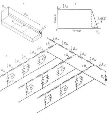
Figure 2.1 a – A “classic” design of a solar cell with a busbar contact, and b – scheme of current flow through a small part of a solar cell ... 23 Figure 2.2 a – The equivalent circuit of an illuminated solar cell with a series resistance, and b – construction of dark and illuminated I-V characteristic of the solar cell with a series resistance ... 27 Figure 2.3 a – A simple solar cell design with a busbar contact and, b – the corresponding multisection equivalent circuit .... 29 Figure 2.4 An example of constructing an illuminated I-V characteristic of a gallium arsenide solar cell assuming the three-section equivalent circuit (Figure 2.3): 1 – the exponential I-V characteristic of each of the diodes; 1’ – the partial-linear approximation of the I-V characteristic; 2 – the illuminated I-V characteristic, in which the bend point position have been calculated by the formulae (2.15) at: Iph = 1 A, Voc = 1.14 V, Rd = 1 Ω, Rs = 0, A = 1, T = 300 K; and 3 – the same, but using
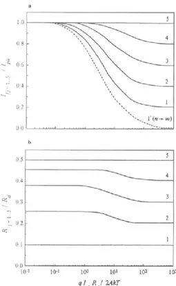
the model of a solar cell with a lumped resistance ... 30 Figure 2.5 Dependences of the values Iij / Iph and Rj / Rd on the generalized argument qIphRd / 2AkT for a five-section solar
cell equivalent circuit. The curve numbers correspond to the values of the index j. Curve 1’ is the dependence of Il1 / Iph at
... 36 Figure 2.6 a, b and c – A family of illuminated I-V characteristics in the coordinates for a modeled gallium
arsenide solar cell at Iph = 2, 10 and 20 A, and d – “dark” I-V characteristic of the p-n junction in a solar cell. The slopes of
the lines 1-5 correspond to the values by the formula (2.31), the slope of the line 1’ corresponds to the value Rs ... 36
Figure 2.7 A general chart of the shape variation of the I-V characteristics and “resistance curves” for a “classic” geometry GaAs-based solar cell in varying illumination intensity (lines a, b, c and d have been constructed for Iph values of 0.5, 20,
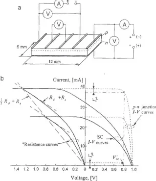
100, and 1000 mA, respectively). The line e is the “resistance curve” for the dark I-V characteristic ... 40 Figure 2.8 a – Design of a GaAs-based solar cell specimen with electric circuits for measurement of Rd , Rs and illuminated
I-V curves, and b – illuminated I-I-V characteristics and the “resistance curves” at two illumination intensities [25] ... 41 Figure 2.9 Geometry of a solar cell (a); its equivalent circuit accounting for the effect of the sheet resistance Rsh and of the
resistance of a metallic contact strip RM (b), and the partial-linear approximation of the illuminated I-V characteristic of one
of the equivalent circuit diodes... 42 Figure 2.10 a – The illuminated I-V characteristic for one of the equivalent circuit branches in Figure 2.9b; b-e – illuminated I-V characteristics of a gallium arsenide solar cell at Iph = 1 A, Rsh = 1 Ω, Rc = 0, A = 1. The magnitudes of RM are,
respectively, 0, 0.25, 0.5 and 0.75 Ω. ... 43 Figure 2.11 A generalized sector of a round geometry solar cell (a), and its three-section equivalent circuit (b) ... 46
x Figure 2.12 Comparison of illuminated I-V characteristics of a solar cell at zero ohmic losses (1); pure lumped losses (2); pure distributed losses in a rectangular geometry of a solar cell (3); and pure distributed losses in a round geometry of a solar
cell (4) ... 48
Figure 2.13 Illuminated I-V characteristics of a gallium arsenide solar cell at Iph = 0.5 A (1) and Iph = 1 A (2). The open circles represent calculation by the formulae (2.42) for a rectangular solar cell at Rc = 0, Rsh = 1 Ω, RM = 0.75 Ω, and the dark circles represent calculation by the formulae (2.44) for a round solar cell at and ... 49
Figure 2.14 Experimental I-V characteristics of a gallium arsenide solar cell of 17 mm diameter under illumination by a flash lamp. Open circles represent I-V coordinates obtained from calculations by the formulae (2.44) at RM = = 2.4 ∙ 10-2 Ω and Rc = = 1.8 ∙ 10-3 Ω, and straight lines represent construction of R0.5 and R0.95 resistances ... 50
Figure 2.15 Experimental I-V characteristics of a high-current gallium arsenide solar cell of 17 mm diameter under illumination by a flash lamp through applied shadowing masks (see the insert). Open circles represent calculation results obtained on the base of the equivalent circuit of Figure 2.12 ... 51
Figure 2.16 The partial-linear approximations of the illuminated I-V characteristics of a solar cell: a – Rs = 0; b, c – Rs > 0. Circles mark the maximum power points ... 53
Figure 2.17 The procedure of calculation of the maximum power point of an approximated I-V characteristic ... 54
Figure 2.18 Dependences of the relative efficiency of the photoelectric conversion in a gallium arsenide solar cell on the generalized argument ; (curve 1); and (curves 2-4, respectively); (curve 5). Curve 6 is the lower boundary of Isc = Iph; and curves 1’ and 1’’ are calculated from the formulae (2.47) and (2.48). The symbols represent the experimental data (see the insert and Table 2.1) ... 55
Figure 3.1 Formation of band tails resulting from random spatial variations of the electrostatic potential caused by the random impurity distribution ... 59
Figure 3.2 Electrical and optical energy gap narrowing versus donor doping density. The curves are based on theoretical calculations; the points are experimental data ... 59
Figure 3.3 The bandgap narrowing reduction factor versus the electron (majority carrier) concentration N for: A-Lanyon Tuft model, B- Hauser model, and C- Slotboom-DeGraaf model ... 62
Figure 3.4 Effective recombination levels ... 64
Figure 3.5 Trap-assisted Auger process in n+ Si ... 64
Figure 3.6 Band-to-band Auger process ... 65
Figura 3.7 Short-circuit current density variation with X ... 67
Figure 3.8 A voltage drop across the base arises at high levels of illumination ... 68
Figure 3.9 Ideality factor variation with X ... 69
Figure 3.10 Saturation current density variation with X ... 69
Figure 3.11 A n+ - p – p+ solar cell with its intrinsic portion identified ... 69
Figure 3.12 Calculated TCR obtained in [50], for n-type silicon as a function of temperature, shown for a range of donor concentrations ... 71
Figure 3.13 Calculated TCR obtained in [50], for p-type silicon as a function of temperature, shown for a range of acceptor concentrations ... 71
Figure 4.1 A pictorial representation of cell surface division in a grid of elements and types of electrical circuits used to represent them ... 73
Figure 4.2 Geometrical properties of a typical subcell ... 75
Figure 4.3 A square-shaped element of solar cell, due to its symmetry, can be divided into four triangles ... 76
Figure 4.4 A rectangular-shaped element of solar cell, due to its symmetry, can be divided into four triangles ... 76
xi
Figure 5.2 Fresnel lens irradiance maps calculated at 400 nm (left), 850 nm (center) and 1050 nm (right) ... 82
Figure 5.3 Parabolic mirror (left) and freeform mirror (right) irradiance maps calculated at 850 nm ... 82
Figure 5.4 Total irradiance profile incident onto the receiver plane for Fresnel lens (top left), parabolic mirror (top right) and Freeform mirror (bottom) ... 82
Figure 5.5 Current map for the system based on Fresnel lens (center), parabolic mirror (center) and freeform mirror (right) 83 Figure 5.6 The comb-like front contact grid pattern with two busbars ... 83
Figure 5.7 IV curves (left) and power curves (right) for the three concentrators ... 84
Figura 5.8 Voltage maps at the emitter surface calculated at the maximum power point, for Freeform mirror (top left), Fresnel lens (top right) and parabolic mirror (bottom) ... 85
Figure 6.1 Interdigitated back-contact structure in a concentrator solar cell ... 86
Figure 6.2 The first 4 steps of the construction of the Koch snowflake ... 88
Figure 6.3 The proposed contact grid; the magnified particular shows 4 of the 5 autosimilarity levels of the figure ... 89
Figure 6.4 The three contact grid patterns considered: comb-like pattern (top left), square-like pattern (top right) and fractal pattern (bottom) ... 90
Figure 6.5 Power curves for the three structures, for a cell ... 92
Figure 6.6 Power curves for the three structures, for a cell ... 93
Figure 6.7 Power curves for square-like structure and fractal structure, for a cell ... 94
Figure 6.8 Voltage maps for comb-like (top left), fractal (top right) and square-like (bottom) patterns for a cell ... 94
Figure 6.9 Voltage maps for comb-like (top left), fractal (top right) and square-like (bottom) patterns for a cell ... 94
Figure 6.10 Voltage maps for fractal (left) and square-like (right) patterns for a cell ... 94
Figure 7.1 Shaded layout of the Cassegrainian concentrator ... 95
Figure 7.2 Structure of an IMS substrate consisting of a metal baseplate covered by a thin layer of dielectric and a layer of copper ... 96
Figure 7.3 Void maps for the four cells obtained by X-ray inspection. The inset on the left side of the figure shows a magnified image of one of them ... 96
Figure 7.4 Temperature map of the cell surface for two different temperatures of sink, 25°C (left) and 45°C (right), for a real-case void distribution ... 97
Figure 7.5 Temperature map of the cell surface for two different void distributions, a 2×2 void matrix (left) and a 10×7 void matrix (right), for a 45°C sink temperature ... 97
Figure 7.6 Power curves of the cell for different sink temperature values for a real void distribution ... 100
Figure 7.7 Maximum power delivered by the cell as a function of temperature ... 100
Figure 7.8 Comparison of cell power curves with and without voids for several values of sink temperature ... 100
Figure 7.9 Current density flowing from cell back contact to ground for the real void distribution (left) and a 2×2 void matrix (right); a current crowding around voids is visible ... 101
Figure 7.10 Current density flowing from cell back contact to ground for a 10×7 void matrix; a current crowding around voids is visible ... 101
xii
List of Tables
Table 3.1 Parameters of an n+ - p silicon solar cell at various concentration ratios, as has been calculated in [42] ... 70
Table 5.1 Main simulation results ... 85
Table 6.1 Parameter values used for the simulations ... 91
Table 6.2 Optimized geometrical parameters of the three structure for a cell ... 92
Table 6.3 Optimized geometrical parameters of the three structures for a cell ... 93
Table 6.4 Optimized geometrical parameters of square-like structure and fractal structure for a cell ... 93
1
1 INTRODUCTION TO CONCENTRATING PHOTOVOLTAIC
(CPV) SYSTEMS
The main problem connected to the use of solar electricity is that it is too expensive. The traditional single-crystal silicon cells require expensive purification limiting harmful impurities to less than 10ppb and expensive crystal growth and cell fabrication steps. Silicon cell efficiencies as high as 23% are achieved when these steps are taken. Unfortunately, these silicon cells and modules and the resultant electricity are then expensive. Meanwhile, when thin-film cells are used with less expensive amorphous or small grain-size materials, the result is low conversion efficiency. While the thin-film modules are then less expensive, the larger installed systems and resultant electricity are still expensive.
The problem is that both low-cost solar collectors and high-efficiency solar converters are needed. Concentrating the sunlight onto efficient single-crystal cells can potentially produce lower-cost electricity by providing a second component. Low-cost plastic or glass lenses or sheet metal mirrors can collect the sunlight and concentrate it onto the expensive high-efficiency single-crystal cells, thereby diluting their cost.
The concentration approach was sponsored for the first time by Sandia National Laboratories. Figure 1.1 shows an approach sponsored by Martin Marietta [3], constituted by an array of point-focus Fresnel lenses focusing sunlight 50 times on silicon cells and Figure 1.2 shows an ENTECH [4] linear arched plastic Fresnel lens focusing sunlight 20 times onto silicon cells. Both systems used aluminum finned extrusions for cell cooling, and both of these pioneering systems operated successfully for several years.
The output power from the point-focus module design shown in Figure 1.1 can be easily improved by replacing the silicon cell with a more efficient multijunction cell. The idea was first developed by Varian [5] in the 1980s. Varian suggested increasing the concentration ratio by using a cell package with a secondary concentrator element. This solution is now implemented in many types of highly-concentrating photovoltaic systems (HCPV).
Under concentrated light, multijunction solar cells achieve efficiencies of over 40%. However, their area-related costs are close to two magnitudes higher than those of bulk silicon solar cells, which clearly dominate the solar cell market today. For terrestrial applications, the high-efficiency multijunction solar cells, usually triple-junction solar cells are used in combination with cheap optics, which collect the sunlight over an area that is several hundred times larger than the solar cell area and focus it on the solar cell. There are four fundamental choices for concentrating optics: refractive (transparent lenses), reflective (mirrored) optical elements, dispersive (holographic, grating and
2 Figure 1.1 The 350-kWp SOLARAS project power plant built and deployed in Saudi Arabia by Martin Marietta using Sandia
Labs technology [1].
Figure 1.2 ENTECH mid-concentration photovoltaic module design using arched linear Fresnel lens [2]
prismatic elements) and fluorescent (panels). Of these, refractive and reflective designs are the most interesting for commercial high-concentration large-scale systems. Several configurations and variations are possible for each of these.
1.1 REFLECTIVE CONCENTRATORS
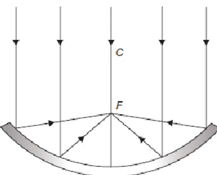
In a reflective concentrator a light ray incident on a smooth mirror surface is reflected as shown in Figure 1.3. As can be seen from the figure, the light ray incident on the surface at angle θ to the surface normal reflects at angle θ’. According to the law of reflection, the angle of reflection is equal to the angle of incidence, θ’ = θ.
Figure 1.4 shows the concentration of the sunlight by a curved mirror surface with radius of curvature R. As can be seen from the figure, the incident rays are concentrated at focal point F. The distance of
3 the focal point from the center of the mirror surface can be calculated from the mirror equation.
Figure 1.3 Schematic representation of reflection.
Figure 1.4 Reflective concentration from a curved surface. The mirror equation is given as
where p is the distance of the light source from the center of the mirror, q is the distance of the concentrated image from the center of the mirror, and R is the radius of curvature of the mirrored surface.
In a concentrated solar system, the distance from the source of light (the Sun) is much greater than the radius of mirror R. It can be said that p is infinity; therefore, . This simplifies the mirror equation to
Now, the image distance or focal length .
Actually, the above equation is an approximation. The mirror surface is really a parabola described by the equation
The equation for a circle is given by
4 This reduces to when and x and . Then, the sunlight incident on a curved mirror surface is concentrated at its focal point, which is equal to half of its radius of curvature R.
1.2 REFRACTVE CONCENTRATORS
In a refractive concentrator light traveling through a transparent medium is bent at the boundary of that medium leading to another medium as shown in Figure 1.5. This is called refraction. As can be seen from the figure, the light ray traveling through the air enters the glass at angle θ1 (angle of incidence)
to the surface normal and is refracted at the top surface to angle θ2 (angle of refraction). The relation
between the angle of incidence and the angle of refraction is given as
where v1 and v2 are the speed of light in air and glass, respectively.
Figure 1.5 Refraction of a light ray passing through a transparent material.
Figure 1.6 Refraction of light rays passing through a plano-convex lens (left) and a Fresnel lens (right).
Refractive index n, a property of any material, can be used to find v for any material. Refractive index n is the ratio of speed of light in vacuum c, and the speed of light in a medium v.
5 In a refractive concentrator, sunlight is concentrated as shown in Figure 1.6. As can be seen from the figure, the light traveling through a plano-convex lens is concentrated at its focal point. The focal length in this case can be calculated approximately from the basic lens equations as follows:
where n1 and n2 are the refractive indexes of air and lens material, respectively. As discussed earlier, p,
the light source (the Sun), is at an infinite distance, and n1 =1 for air. The equation simplifies to
Now, the image distance or focal length
, where n = n2 is the refractive index of the lens
material.
As noted above, the refraction occurs only at the surface of a lens. Taking advantage of this fact, a thin lens (called a Fresnel lens) was developed and serves the same purpose as a thick lens. Fresnel lenses are being used in many applications as a less expensive and weight-reducing alternative to thick lenses. Fresnel lenses made from acrylic polymers for nonimaging applications such as CPV systems can further reduce the cost of a refractive concentrator system. Concentration of sunlight through a Fresnel lens is shown in the right side of Figure 1.6.
1.3 FRESNEL LENS
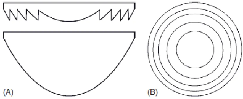
Fresnel lenses are the principal choice for refractive systems due to the weight, low material content and low internal absorption compared to spherical or aplanatic lenses. A top view of a typical Fresnel lens is showed in Figure 1.7.
6 Plastic materials are the choice for solar concentrators due to their low cost and the ready availability of mass-production molding or stamping technologies. Silicone molded on glass substrates to form the Fresnel lens is also an emerging approach. Fresnel lenses, however, suffer from chromatic aberrations, which become more pronounced for the larger aperture lenses needed at higher concentrations. Chromatic aberrations create a local mismatch between the currents of the subcells of a triple-junction solar cell pulling down the efficiency.
Basically, a Fresnel lens has optical properties similar to conventional lenses; however, they have lower material usages and therefore lower intrinsic cost. This is due to the fact that a Fresnel lens is obtained by breaking a conventional lens into a set of concentric segments. Figure 1.8 shows a sketch of a conventional and planar Fresnel lens with the same size and focal distance. As a result of the faceted structure, a Fresnel lens offers an additional dimension in design space. The angle of each facet can be varied in order to decrease spherical aberration or the homogeneity of the light distribution in the focal spot [6].
Figure 1.8 (A) A sketch of the cross section of a conventional lens and above a corresponding Fresnel lens with the same
size and focal length. (B) The concentric segments of the Fresnel lens are sketched in a plan view.
The relatively low manufacturing and material costs makes Fresnel lenses one of the cheapest available concentrating optics. This is the reason why they have been used from the beginning of PV concentrator development and are the most widely used optical system in CPV today.
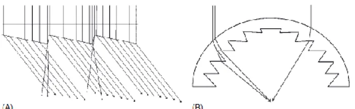
In comparison to a massive lens, however, a Fresnel lens has to pay some additional efficiency losses. A Fresnel lens consists of many prismatic facets that refract the light onto the focal spot. Ideally each facet has a sharp peak and valley, and the groove wall is oriented parallel to the sunrays. However, the real structure of a Fresnel lens shows deviations, for example, due to the manufacturing process, which lead to losses. These losses are sketched in Figure 1.9a and are summarized in the following points:
1. The light impinging on rounded facet peaks or valleys is not concentrated and lost. In order to minimize these losses, accurate manufacturing technique and large facet spacing relative to the total size of the lens are mandatory.
7 groove wall. In practice, this wall must be slightly tilted in order to provide a reliable de-molding during the manufacturing. This tilting causes some rays to be misguided.
3. For simplicity and manufacturing reasons, the active side of a facet does not have the most ideal bent shape but is approximated linearly. The resulting losses are negligible when the facet spacing is small compared to the total size of the lens.
However, when closed facet spacing is used, diffraction effects can decrease the optical efficiency of the Fresnel lens. These losses can become significant at facet diameters around 100 μm.
In addition to the loss mechanisms specific to the Fresnel lens, the typical optical losses for lenses like aberration, absorption, scattering at surface imperfections and surface reflection must be considered. Reflection losses at surfaces can be reduced with appropriate antireflection coatings; however, these coatings increase the cost of the Fresnel lens.
For imaging optical elements, the maximum achievable concentration is determined by the ratio of focal length and diameter of the optics; this follows from the ètendue. A flat Fresnel lens designed for high concentrations must refract light rays impinging the corner of the lens in a steep angle. This increases the chromatic aberration of the lens, and in extreme cases rays from the lens corners are lost due to total internal reflection. Thus, the maximal concentration of a Fresnel lens is limited by the chromatic aberration and reflection losses. The exact limit depends on a number of parameters (e.g., the refractive index). Typically, the maximum concentration limit is quoted to be about 500X for flat Fresnel lenses [7]. For geometric concentrations < 500X, the optical efficiency of a Fresnel lens usually ranges between 70% and 90%, depending on the quality of the manufacturing process.
An additional design parameter for a Fresnel lens is the surface curvature. In Fresnel dome lenses, the light rays are refracted at two surfaces, as is shown in Figure 1.9B.
Figure 1.9 (A) A typical loss mechanism of a flat Fresnel lens are sketched. In practice, the active side of each facet refracts
incoming light rays toward the focus. Ideally, the shape of a facet is hyperbolic; however, in practice, it is often approximated linearly. Typically, light rays are misguided at peaks and valleys of the facets, which cause a decrease of the optical efficiency. Furthermore, the groove wall of each facet is typically slightly tilted in order to provide a reliable de-molding during the manufacturing process. This also has a negative impact on the optical efficiency of the Fresnel lens. (B) A dome Fresnel lens is sketched. As a result of the bowed surface structure, the light rays are refracted at two surfaces. Thus, direct light rays can be refracted in a relative steep angle at comparable low reflection and aberration losses. Furthermore, when direct light is impinging perpendicularly on the dome Fresnel lens, the grooved side of the facets and the peaks does not impact the light rays. Consequently, these parts of the domed Fresnel lens do not decrease the optical efficiency .
8 Consequently, the required angles of refraction are smaller for a Fresnel dome lens than for a flat Fresnel lens with the same size and focal length. Using a Fresnel dome lens, short focal lengths and comparatively low chromatic aberration can be realized. This, in turn, allows higher concentration ratios to be achieved as compared with flat Fresnel lenses.
A problem connected to the use of Fresnel lenses is that the spatial distribution of light at the focal spot is inhomogeneous. This can have a negative impact on the solar cell performance, as we will see in this thesis. In Figure 1.10 the measured spatial intensity distribution in the focus of a flat Fresnel lens with a lens aperture of 16 cm2 is shown [8]. The central peak intensity decays to 10% at a distance
of 0.6 mm from the center. This Fresnel lens is used together with a circular 2 mm cell, leading to a geometric concentration ratio of 500X. However, the real central peak intensity can reach concentration ratios above 2500X.
For these reasons, in order to compensate for these disadvantages, secondary optical elements are often applied in CPV modules with flat Fresnel lenses.
1.4 SECONDARY OPTICS FOR FRESNEL LENSES
A second optic provides a second chance to influence the path of the light rays. Usually, secondary optical elements are located close above the solar cell. The task of a secondary can be manifold. In particular, it can increase the concentration ratio and/or the angular transmission. If required, it can homogenize the spatial distribution of concentrated sunlight on the solar cell. A simple secondary approach for Fresnel lens concentrators was already used in a 200X Fresnel lens concentrator of the Sandia National Laboratories [9]. There, a highly reflective cone was located around the cell in order to catch spilled sunrays. Also in more recent developments at Fraunhofer ISE, the potential of a reflective cone secondary was investigated. In particular, these elements are manufactured from Al, which are equipped with metallic reflector layers [10]. The reflective cone secondary has been designed that only misguided light rays from the primary optics are concerned. Thus, this type of secondary is expected to have only a positive impact on the optical performance of the concentrator. Figure 1.11A presents the short-circuit current of two FLATCON test modules versus the angle of misalignment. Each of the two modules consists of six 4.15 mm2 triple-junction solar cells which are
placed in the foci of 40 × 40 mm2 Fresnel lenses. One of the modules was, in addition, equipped with
reflective secondary optics. Obviously, the gain in optical performance increases with higher angles of misalignment.
It is important to note that the solar disk has an angular size of about ±0.25°. The direct irradiation incoming within an opening angle larger than ±0.25° is called circumsolar irradiation, and the intensity is typically 5-20% of the direct sunlight [11] (circumsolar ratio or CSR), depending on
9 Figure 1.10 A profile of the measured intensity in the spot of a 40 × 40 mm2 Fresnel lens is shown. The measurement was
carried out with monochromatic light at a setup developed at the Fraunhofer ISE [18].
Figure 1.11 (A) The angular transmission of two test modules with six Fresnel lenses (40 × 40 mm2) and six solar cells (4.15 mm2) is shown. In principle, both modules have the same components, except for an additionally mounted reflective secondary optic on one of the modules. The short-circuit current of the modules was measured outdoors under a varying
sun vector angle. (B) A photo of a test module equipped with reflective secondary elements is shown.
atmospheric conditions. As can be seen from Figure 1.7A the CSR is poorly utilized by the Fresnel lens. Obviously, the reflective cone secondary offsets this disadvantage and the direct sunlight and the CSR can be utilized more efficiently.
For small angles of misalignment, the gain in optical transmission is relatively small and the secondary does not avoid a significant drop in optical transmission at a misalignment angle of 1°. This is a result of light reflection losses in the secondary.
Alternatively to simple cone reflectors, secondary optics, which use total internal reflection, can be applied. These are dielectric optical elements that have to be placed in the concentrated beam of the Fresnel lens. At the entrance aperture, the light is refracted into the secondary and is total internally reflected at the side walls of the secondary. Finally, the light leaves the secondary at the exit aperture.
10 Usually, the exit aperture and the solar cell are connected with an optical coupling medium in order to decrease reflection losses at the surfaces. Depending on the surface quality, total internal values of up to 100% can be achieved and the angular transmission of the Fresnel lens concentrator can be increased significantly. The refraction of light at the entrance aperture provides an additional degree of freedom in optical design. However, losses occur due to surface reflection and absorption in the secondary dielectric material.
Typical representative of total internal reflection secondaries are Compound Parabolic Concentrators (CPCs) and light rods. The latter usually has a conical shape with an entrance aperture larger than the exit aperture and can be used for homogenizing purposes.
A CPC is a nonimaging concentrating optical element that can allow high concentration ratio and high angular transmission values [12]. The side of a CPC is shaped parabolically and the entrance aperture is larger than the exit aperture, as is shown in Figure 1.12. Beneath a Fresnel lens, it can be used to increase the concentration and the angular acceptance of the concentrator. Ray-tracing simulations show that with a Fresnel lens and a CPC secondary, a concentration of 1000X and an acceptance angle of 1° can be achieved.
Figure 1.12 A typical CPC and its section view
Furthermore, already in the mid 1980s, the Varian Research Center used a conical glass element with a convex-shaped entrance aperture as secondary element. This provided a second refraction of the beam focused primarily by a Fresnel lens. In addition, a total internal reflection guided the light rays on the cell. Due to this advanced secondary concept, a Fresnel lens concentrator with a concentration factor of almost 1000X and an outstanding angular acceptance of more than 1° could be realized [13]. The modules used GaAs single-junction concentrator solar cells, achieving an efficiency of about 28% [14]. Furthermore, a module efficiency of 22.3% was reported, which was achieved with a Fresnel lens concentrator equipped with 12 GaAs solar cells and without applying a temperature correction [15]. Considering this concentrator would have been equipped with today’s triple-junction solar cells instead of the single-junction cells, one could expect a module operating efficiency of about 30%.
11
1.5 CENTRAL RECEIVER REFLECTORS
Central receiver reflectors are another popular approach to concentrator systems [16]. These systems employ a single, large reflective dish, constructed from multiple mirror segments, to focus the sunlight on a dense array of solar cells. Central receiver optical systems have high efficiencies but very narrow acceptance angles and therefore require accurate tracking systems. Furthermore, the solar cells must be actively cooled, since the back-side area, which is to say the area available to conduct heat passively to the environment, is small compared to the entrance aperture. Active cooling consumes system power and adds an additional level of complexity to system construction and maintenance. In recent years, the optical ad thermal difficulties of lens and dish concentrators have been overcome through the use of arrays of small-aperture mirrored concentrator systems. Although these systems are slightly less efficient than a single-mirror system, the Cassegrainian two-element lens system confers several advantages on a solar concentrator system: 1) the folded optical path is more compact than a single-element lens; 2) higher efficiency and concentration than a Fresnel lens; 3) absence of chromatic aberrations. Since the focal point is positioned between the two elements and can be positioned near the apex of the primary element, the cell with its heat sink can be placed at that point. With the cell heat sink proximate to the assembly backpan, efficient thermal dissipation to the air becomes simple. For these reasons at the Physics Department of the University of Ferrara an important part of the research activity is oriented to the creation of prototypes of Cassegrainian concentrator systems.
1.6 OPTICAL DESIGN OF A CASSEGRAINIAN CONCENTRATOR
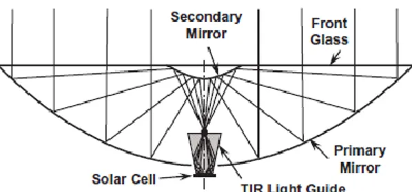
Several practical design goals influence the detailed configuration of a Cassegrainian optic for use in concentrating panels. Ease and economy for automated manufacturing, module compactness, passive cooling, and reasonable optical tolerances that facilitate tracker design are foremost. Furthermore, minimizing secondary mirror shadowing and accurate alignment of the two mirrors during manufacturing form additional constraints. Usually secondary mirror shading is chosen to be < 4% to retain reasonable system efficiency; this leads to optical constrains that position the focal point between the primary mirror apex and the secondary mirror. However, it is advantageous to place the cell and heat sink at or below the apex of the primary mirror to facilitate heat transfer to the backpan. These conflicting constraints can be overcome by inserting a nonimaging TIR light guide between the focal point and the cell, permitting cell placement behind the focal point. Concurrently, tailoring the light guide design may either expand the acceptance angle or permit higher concentrations. Figure 1.13 compares the focal position at 0° and 1° pointing error at the entrance to the light guide [1].
12 The diagrams are taken from ray trace models of the incoming light through the full Cassegrainian optical system. The cell active area position is also indicated in relation to the light guide entrance, with the relative intensity of the light at the focal point indicated by concentric circles. It can be seen that at higher deviation angles, light that would otherwise fall off of the cell is guided back to the active area through TIR at the guide walls.
Without the guide, only a much larger cell would intercept off-track rays effectively. Alternatively, the same size cell could be employed but with far more stringent demands placed upon the tracking system. The use of a light guide as tertiary optical element results in lower cell costs, more efficient thermal management and less onerous tracker requirements. Since the optical focal point corresponds to the top of the light guide, any unintentional defocusing protects the optics by lowering, rather than raising, the optical flux on the guide. In the event of gross pointing errors, the focal point is well above the primary mirror, thereby averting severe damage to the mirror while maintaining the concentrated flux safely within the panel.
The resulting design is shown in Figure 1.14, while Figure 1.15 shows a Cassegrainian concentrator prototype, made of four modules, realized at the Physics Department of the University of Ferrara.
Figure 1.13 Modeling of focal point for 0° (a) and 1° (b) pointing error. At 0°, all the light strikes the cell; with no guide, a 1°
pointing error moves nearly all the focused light fully off the cell; with the guide, all of the light is reflected back onto the cell active area.
Figure 1.14 Cross section through the center of the optics for an aplanatic Cassegrainian optical system with tertiary
13 Figure 1.15 Cassegrainian concentrator prototype realized at the Physics Department of the University of Ferrara
1.7 CASSEGRAINIAN CONCENTRATOR SYSTEM FEATURING SPECTRAL
SPLITTING
The HCPV Cassegrainian optical configuration offers an additional opportunity for increasing collection efficiency. Through the use of dichroic filters it’s possible to split the solar spectrum into a number wavebands and to direct each filtered light beam towards suitable cells. For example the dual-focus Cassegrainian solar concentrator module concept, which was first described and developed by Fraas and Shifman et al. [17-18], uses a dichroic secondary mirror to split the solar spectrum into two parts and to direct the IR and near-visible portions of the spectrum to two separate cell locations. The second solar cell is located behind the dichroic secondary as shown in Figure 1.12. This is an important method for harvesting lost energy stemming from the current imbalance present in multijunction solar cells, or for utilizing materials and bandgap combinations not otherwise available. As shown in Figure 1.16, the first version of this solar concentrator PV module used InGaP/GaAs double-junction cells located at the near-visible focus at the center of the primary and GaSb IR solar cells located behind the secondary.
The spectral splitting approach introduces two key advantages: 1) for each waveband a suitable solar cell with optimal bandgap can be used, in order to increase the conversion efficiency; 2) separate cell locations divide the heat load so cells work cooler at higher-efficiency points.
The first advantage is demonstrated by the use of the InGaP/GaAs and GaSb cell set rather than the traditional InGaP/GaAs/Ge monolithic triple-junction cell. Unfortunately, the three materials in the monolithic junction cell do not have the ideal bandgap energies for an ideal monolithic triple-junction cell. The Ge bandgap energy is too low, generating excess current compared to the other two junctions. The excess current is wasted as heat. In contrast, the higher bandgap GaSb IR cell generates
14 a higher voltage, and the separate electrical connection extracts all the power produced. Overall module efficiency is thereby increased.
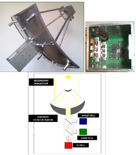
The spectral splitting approach is being adopted at the Physics Department of the University of Ferrara; Figure 1.17 shows a tricroic Cassegrain concentrator. It makes use of three different receivers: InGaP, GaAs and Si. Cross section shown in Figure 1.13 illustrates its working principle. Receivers are placed in a box at the back side of the primary mirror; in this way fin heat sinks can be easily mounted at the box walls.
Figure 1.16 Dual-focus Cassegrainian PV module with dichroic secondary for use with separate multijunction solar cells.
The system makes use of two dichroic filters, 45° tilted, placed in the receiver box. The first receiver reflects the portion of the spectrum with λ < 650 nm and direct it onto the InGaP cell, while the second dichroic filter reflects the portion with λ < 850 nm and direct it onto the GaAs cell. The remaining part of the spectrum is transmitted through both filters and reaches the Si cell. Suitably optimized, this system is expected to reach 30 % efficiency.
1.8 INTRODUCTION TO CONCENTRATOR SOLAR CELLS
In this section we will review the main physical mechanisms that govern the operation of a semiconductor solar cell. Since such a kind of devices are essentially p-n junctions suitably engineered, in our analysis we will assume that the electrical properties of p-n junction are known and we will concentrate on what happens when a p-n junction is illuminated.
For the sake of simplicity we assume a monochromatic illumination of the cell, from the p-material side, with an energy of the photons such that hν = EG. Furthermore, we assume that electron-hole pairs
are generated only in the p-region at a distance from the p-n junction shorter than the electron diffusion length.
In order to comprehend the behaviour of a p-n junction under illumination we can consider three different cases: the short-circuit condition, the open-circuit condition and the case when an external
15 Figure 1.17 Tricroic Cassegrainian concentrator realized at the Physics Department of the University of Ferrara. Overall
structure (top left), box containing the three receivers placed at the back side of the primary mirror (top right) and pictorial representation of the working principle (bottom)
load resistance is connected to the cell terminals [2]. The three cases are schematically represented in Figure 1.18.
Figure 1.18 The band energy diagram of a p-n junction under illumination: in the short-circuit regime (left), in the
16 In the short-circuit regime the external connection provides a zero potential difference between the n- and p-regions, so that the band energy diagram is equal to the band diagram of a p-n junction at thermodynamic equilibrium (without illumination and without bias voltage). In this case, however, a photogenerated current flows through the circuit. Electrons collected by the p-n junction at the n-side reach the back metal contact at the n-side and flow through the external wire. When they reach the interface between metal and the p-region they recombine with the photogenerated holes.
It is important to note that the energy diagrams of the n- and p-regions in the vicinity of the contacts correspond to the ideal non-rectifying (i.e. ohmic) contacts between a metal and a semiconductor without a barrier for the carrier flow-over. This situation can be arranged by more heavy doping the n- and p-regions in the vicinity of the contacts, so that EC – EF and EF – EV would be equal to zero, and
also by choosing metals characterized by the corresponding Fermi level energy positions, similar to those in the semiconductor.
At open-circuit-regime electrons entering the n-region collect there and charge it negatively. At the same time, holes entering the p-region charge it positively. The resulting potential difference is called open-circuit voltage VOC. This case is shown in the center part of Figure 1.1.
The VOC magnitude is always less than the contact potential VC, so that always exists a little step ΔEC
on the p-n junction diagram; this means that the potential energy of electrons near the conduction band bottom is lower in the n-region than that in the p-region. This fact is essential for an effective extraction of photogenerated electrons from the p-region into the n-region. The photocurrent Iph
doesn’t depend on the p-n junction bias voltage. It can be expressed as the number of photogenerated carriers passing through the p-n junction in a unit time:
where Pr is the incident monochromatic radiation power. Obviously, we are assuming that each
incident photon generates an electron-hole pair; this condition is usually met satisfied for solar cells based on Si and GaAs.
At short-circuit regime, the short-circuit current is equal to the photocurrent:
Under open-circuit conditions the photocurrent is in equilibrium with the “dark” current Id, the forward
current produced by the p-n junction when it is biased with a potential difference Voc. So we have:
From (1.10) it’s possible to find an expression for Voc (at )
17 The “dark” current is accompanied by recombination of minority carriers (in our case electrons in the p-region). At recombination potential energy of electron-hole pairs is either released by means of emission of photons with hν ≈ EG (radiative recombination), or dissipated as heat in the crystal lattice.
Radiative recombination is represented in Figure 1.1 with arrows.
In order to find a general expression for the I-V characteristic of an illuminated p-n junction, we assume that a power generator is connected to the junction terminals. At a positive bias voltage the photocurrent is subtracted from the “dark” current, and at a negative one is summed to it. Assuming the direction of Iph as positive, we can write:
where Vl is the voltage drop across the load resistance and Il is the current flowing through it. Figure
1.19 shows an I-V characteristic of a solar cell [2]. Only portion of the curve in the second quadrant is shown, since only there the cell acts as a power source, since the direction of the current is “opposite” to the applied voltage polarity. Load resistance I-V characteristic is given by:
Figure 1.19 also shows load resistance I-V characteristics for different values of Rl itself.
Figure 1.19 Illuminated I-V curve of a p-n junction in GaAs and I-V characteristics of load resistance Rl for different
magnitudes of Rl, 0.1 Ω (1), 1.026 Ω (2) and 10 Ω (3).
Now we can calculate output electric power in the load resistance:
Since in both short circuit and open circuit regimes P = 0, for either Vl orIl is equal to zero, there
exists some optimum value of Rl = Ropt, at which the cell provides its maximum output power. To find
the corresponding values of Vl = Vm and Il = Im, we have to solve the equation :
After some rearrangements we obtain [1]
18 Equation (1.16) can be solved by the successive approximations method. Two calculations are enough to obtain four correct significant figures. Substituting Vm into the (1.12) we obtain
Thus it’s possible to determine and, finally, Pm:
The value of Pm corresponds to the area of the crosshatched rectangle in Figure 1.2.
The fill factor (FF) of an I-V characteristic is a parameter evaluating its “quality”:
Fill factor quantifies how much the shape of an I-V characteristic of a solar cell is close to a rectangle. In this thesis several works based on concentrator solar cell numerical simulation will be presented. In all of them fill factor has been taken into account as figure of merit of the cell, since it is a parameter that gives an overall view of the cell working conditions.
The above obtained expressions allow us to better understand the fundamental physical parameters that limit the efficiency of an ideal solar cell [2].
The expression (1.18) can be rewritten as
where is the energy calculated for each absorbed photon, which is transferred to the load resistance at an optimum matching of the p-n junction and the external circuit. Rearranging the expression (1.21) it’s possible to highlight the factors having effects on the value of Em. Substituting in (1.14) the expression
for Voc given in (1.11) and the following expression for i0 reported in [2]:
we obtain, after a further rearrangement
Equation (1.16) shows that the energy gap Eg, defining the potential energy magnitude of one
photogenerated electron-hole pair, is the upper estimation limit for Em. The second term in the curly
brackets represents in (1.23) represents losses of a fundamental character, constraining efficiency of a solar cell. The first two addenda in the curly brackets reflect the fact that the contact potential difference Vc is lower than than the magnitude of Eg / q [2]. The “losses due to Vc” depend on the
19 density of states in the valence and conduction bands of a semiconductor, and also on the majority carrier concentrations in the n- and p-regions of the p-n junction. The third addendum reflects the fact that Voc<Vc. This kind of losses depend on the majority carrier concentration and electrophysical
parameters (mobility, diffusion lengths) of the minority carriers in the n- and p-regions of the p-n junction. The fourth addendum depend on the three previous addenda (see the expression (1.16)) and reflect the fact that Vm<Voc. Finally, the fifth addendum (kT multiplied by unity) can be interpreted as
“losses due to optimum current”, and depend on the fact that the current Im is less than the
photocurrent (see the expression (1.17)).
Keeping in mind that a monochromatic illumination of the p-n junction has been supposed, the conversion efficiency can be defined as the ratio of Em to the energy of one absorbed photon hν:
As is known, sunlight is not monochromatic; solar cell parameters, especially the energy gap Eg, has to
match the real solar radiation spectrum.
As is known, the longest wavelength λg, starting from which photons can be absorbed in the solar cell
material with the energy gap Eg, is
Photons with longer wavelength are not absorbed in the semiconductor and their energy is lost from the point of view of photovoltaic conversion.
Conversely, photons with an energy hν > Eg, produce “hot carriers” which, in addition to the excess
potential energy Eg, gain the excess kinetic energy equal to the difference hν - Eg. However, this
kinetic energy is rapidly spent heating the crystalline lattice. Thus only photons from a high-energy part of the spectrum are absorbed by the semiconductor, and only part of the energy of these photons is converted into the potential energy of the electron-hole pairs. Knowing the spectral distribution of the photon flux incident onto the cell surface it’s possible to obtain the photocurrent density produced by the cell in the following way:
From (1.26) it can be deduced that, for a given spectral photon distribution, i.e. for a given solar radiation spectrum, photocurrent density decreases at increasing energy gap Eg of the p-n junction
material. Figure 1.20 shows the dependence of iph on Eg for the solar spectra AM 0 and AM 1.5D [2].
The maximum energy utilized in the load for one absorbed photon (Em in (1.23)), rises initially with
increasing Eg and then starts to decrease when the change of the term containing iph becomes
substantial.
20 Figure 1.20 Dependences of the photocurrent density on the energy gap Eg, for the spectra AM 0 and AM 1.5D.
A known method of calculation of Em is based on thermodynamic considerations [19-21]. A
semiconductor solar cell, being in thermodynamic equilibrium with the surroundings, exchanges energy by means of radiant emission and absorption. The equilibrium black-body radiation which always exists inside a solar cell material at a given temperature defines the lower limit of the saturation current density i0 in the p-n junction. According to [11], i0 is given by:
where n is the refractive index of the solar cell material. Physically, this expression presents i0 as “ a
photocurrent generated by the intrinsic black-body irradiation”. For its calculations the spectral distribution of the black-body radiation at the solar cell temperature is used, the contribution to i0
being given by photons with hν ≥ Eg. Then, knowing iph, one can find Voc from (1.11), Em from (1.21)
and “monochromatic” efficiency from (1.24) at hν = Eg. These values of efficiency are depicted in
Figure 1.21 by the lines 2, 3, 4 for three magnitudes of iph.
The wavelengths in the abscissa should be considered as that corresponding to Eg for individual
semiconductor materials, as given in (1.25). For a chosen material the conversion efficiency magnitudes for light with wavelengths shorter than λg have to be reduced λg/λ times, which is pictured
in the figure by three tilted straight lines for three semiconductor materials (In0.5Ga0.5P, GaAs and Ge)
and iph = 1 A∙cm-2. The conversion efficiency of a solar cell based on a chosen material can be
obtained by multiplication of magnitudes taken from the corresponding tilted straight line by the solar spectrum, and then by integration over wavelengths up to λg. The energy spectrum AM 0 is depicted in
Figure 1.21 by the curve 1, and the results of multiplication for the above mentioned materials by the curves 5, 6, and 7. Thus the thermodynamically limited maximum value of the efficiency ηmax for an
idealized solar cell on the base of each chosen material is taken as the area enclosed by curve 5, 6, 7 when the area enclosed by curve 1 corresponds to 100%.
21 Figure 1.21 Curve 1 – the energy spectrum AM 0 for non-concentrated sunlight; lines 2, 3 and 4 – plots of maximum
monochromatic efficiency off an idealized solar cell for iph = 0.1; 1 and 10 A∙cm-2 respectively; sloped lines – spectral
dependences of conversion efficiency in the idealized solar cells based on In0.5Ga0.5P, GaAs and Ge, at iph = 1 A∙cm-2; curves
5, 6 and 7 show the portion of solar energy converted into electricity in the corresponding solar cells.
photocurrent density, i.e. with concentration of sunlight.
If we denote the Sun concentration ratio as KS, calculated magnitudes of at conversion
of non-concentrated (Ks=1) and concentrated (Ks=1000) sunlight are presented in Figure 1.22. AM 0
and AM 1.5D spectra have been considered. As can be seen from the figure, silicon and gallium arsenide have an energy gap magnitude that fall just into the range of the highest values of ηmax.
Figure 1.22 Maximum thermodynamic conversion efficiency of a solar cell made of a material with an energy gap Eg, where
T = 300 K. 1, 1’ – Ks = 1; 2, 2’ – Ks = 1000; 1, 2 – for the Sun spectrum AM 0; 1’, 2’ – for the Sun spectrum AM 1.5D.
The maximum efficiency is about 31% for Ks = 1 and 37% for Ks = 1000 (AM 1.5D). These limits,
22
2 OHMIC LOSSES IN SOLAR CELLS
Ohmic losses in solar cells basically arise from the fact that semiconductor and metal layers by which a solar cell is made of are characterized by a non-zero resistivity value. As a consequence, as in any electric generator, in a real semiconductor solar cell a part of the generated power is dissipated at the internal resistance. Solar cells for conversion of concentrated sunlight have to be designed in such a way that internal ohmic losses are drastically reduced. Production of high-current high-efficiency solar cells implies an accurate choose of parameters of a semiconductor structure and of a solar cell design as a whole, taking into account optical, recombination and ohmic losses.
In the related literature there is no universally adopted procedure for the description and measurement of the ohmic losses in solar cells, despite the fact that solar cells have been used, for instance, in power supply systems for spacecrafts for almost forty years.
In this chapter, taken from [2], various aspects related to ohmic losses will be discussed in detail. Such a description will allow us to gain a deep insight into the problem. Several solar cell models with lumped and distributed parameters will be considered. An analytical approach will be developed in order to calculate illuminated current-voltage characteristics with known values of the internal resistance components.
2.1 INTERNAL RESISTANCE PROBLEM
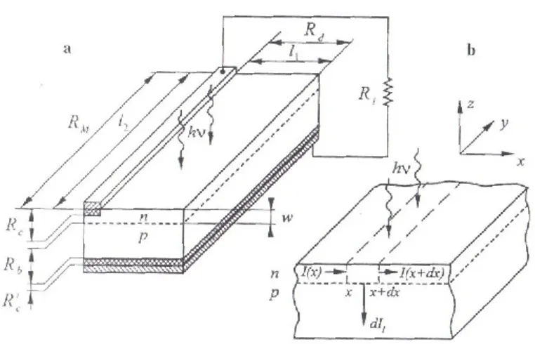
Fig. 2.1a shows a simplified version of a typical solar cell geometry, that is a rectangular semiconductor wafer with a planar p-n junction. On the illuminated side a busbar contact is situated, and on the back side a solid one. It is assumed that incident light is uniformly distributed on the whole light-sensitive surface. Furthermore, every incident photon generates electron-hole pairs, which are then separated by the p-n junction.
In their travel towards the busbar contact, the photogenerated carriers overcome the sheet resistance of the p-n junction front region (the n-region in this case), then the metal-semiconductor contact resistance (the resistance of an intermediate region between the n-type layer and the busbar contact) and the resistance of the metallic contact strip. The resistance of the base region of the solar cell (the p-region in this case) and the contact resistance on the back surface are connected in series to the external load. In many types of solar cells intended for conversion of concentrated sunlight the resistances of the base region and of the back contact don’t constrain the output power, since the base region may be highly doped and the back contact area is much larger than that of the contact grid on the front surface. The relations between the main resistance components (the sheet resistance, the
23 contact resistance and the resistance of the strip) and the recombination and optical losses can be considered as follows. The sheet resistance of the solar cell n-region can be reduced, for instance, by increasing its thickness w.
Figure 2.1 a – A “classic” design of a solar cell with a busbar contact, and b – scheme of current flow through a small part of
a solar cell
However, this will result in an increase in the recombination losses, because collection by the p-n junction of holes generated by light in the vicinity of the surface will not be so effective. The same result may also be caused by increasing electric conductivity of the n-region at the expense of an increase in the doping level. What is more, the possibility of decreasing the resistance in such a way is restricted by the solubility limit of donor impurities and by their capability to create new free electrons. One may reduce radically the n-layer resistance by decreasing the solar cell size l1 or by
making several parallel contact strips connected with each other with an additional bus. However this will lead to an increase in the optical losses, for a significant part of the light-sensitive surface appears to be covered by the contact grid. In the solar cells intended for conversion of non-concentrated sunlight grid fingers are spaced 2-5 mm apart for a resulting shadowing coefficient of about 5%. In this case the grid pattern is prepared by the silk screening technique. In the high-current solar cells finger spacing is reduced to 0.1-0.3 mm, which requires application of a photolithographic process. For such solar cells the shadowing coefficient may approach 10-15%.
The magnitude of the contact resistance decreases with increasing contact area, however the optical losses tend to be higher. This resistance depends on the choice of metal (or alloy) for the contact and on the technology of metal deposition and thermal treatment. Such metals as Ni, Ag, Au, Pd, Cr, Al (for Si) and also combinations of layers of these metals are more widely used for making contacts to solar cells based on Si and GaAs. The deposition processes are vacuum deposition, chemical deposition, electroplating, or painting with a paste containing a metallic powder. Temperature and
24 duration of the thermal treatment also have an essential effect on this magnitude. The critical factor in this case is a risk of melt-through of the thin front region of the p-n junction. Let’s consider an action of the sheet resistance of the front region in a solar cell which has a distributed nature regarding to the area of the p-n junction. We shall characterize it by its value Rd:
where ρ is the resistivity of the front layer material; w is the layer thickness; and l1 and l2 are the solar
cell dimensions across the contact strip and along it, respectively. Let’s make the following assumptions: w and the contact strip width are much smaller than l1; the contact resistances Rc and R’c
are equal to zero; the longitudinal resistance of the metallic strip ; the base resistance Rb = 0.
In this case it can be assumed that the potential V of the p-n junction front region change only along the x-axis normal to the contact strip.
To deduce we shall consider a section of a solar cell of width dx (see Figure 2.1b). Part of the load current flows through the p-n junction section of width dx, i.e.
The equation for the current flowing along the front layer has a form
According to Ohm’s law, the current is defined as the ratio of the varation in potential to the resistance of the section dx (defined similarly to equation (2.1)). Hence, allowing for the decrease of V along x
In the same way one may write an expression for . Then using equation (2.2) after regrouping the terms we can rewrite equation (2.3) in the form
![Figure 1.2 ENTECH mid-concentration photovoltaic module design using arched linear Fresnel lens [2]](https://thumb-eu.123doks.com/thumbv2/123dokorg/4724967.45820/11.892.261.635.82.336/figure-entech-concentration-photovoltaic-module-design-arched-fresnel.webp)