https://doi.org/10.1007/s10854-020-03886-7
A study on CdCl
2activation of CBD‑CdS films
W. G. C. Kumarage1 · R. P. Wijesundera2 · V. A. Seneviratne3,4 · C. P. Jayalath3,4 · N. Kaur5 · E. Comini5 · N. Gunawardhana1 · B. S. Dassanayake3,4
Received: 12 April 2020 / Accepted: 26 June 2020
© Springer Science+Business Media, LLC, part of Springer Nature 2020
Abstract
Cadmium sulfide (CdS) thin films were deposited using chemical bath deposition (CBD) technique on fluorine-doped tin oxide glass substrates. Cadmium sulfate, thiourea, and ammonium hydroxide were used as Cd source, S source, and the complexing agent, respectively in the reaction bath. The post-deposition CdCl2 activation of chemical bath deposited CdS (CBD-CdS) thin films was done by dip coating in a saturated CdCl2 bath. X-ray diffractograms show the growth of large CdS grains with better crystalline quality over the recrystallization process due to CdCl2 treatment. The development of large clusters was determined to be due to coalescence of smaller clusters. The photoelectrochemical (PEC) cell (CdS/Na2S2O3/ Pt) parameters, such as VOC and ISC for CdCl2 activated CBD-CdS thin films were found to be higher compared to untreated CBD-CdS thin films. The improved effective surface area of the film and higher carrier concentration due to grain bound-ary passivation could be the reason for higher VOC and ISC values found in CdCl2-treated CdS films. Additionally, all the CdCl2-treated CdS films showed an increase in the optical transmittance spectra and bandgap compared to untreated CdS films. Relative energy band edge position of the grown CdS films was found to be adjustable with the CdCl2 treatment time. The best photoactivity was found for the CdS films which were dip-coated for 10 min in CdCl2 solution.
1 Introduction
Polycrystalline CdS thin films have shown potential pho-tovoltaic applications due to its direct bandgap, high trans-mittance, low resistivity, and relative ease of film growth [1, 2]. Among the dozens of growth techniques, chemical bath deposition (CBD) is considered as a favored technique of CdS thin film deposition due to its simplicity, low cost, adaptability, and reliability [3–8]. Additionally, the effect on growth kinetics, deposition bath temperature, chemical concentration, film thickness, and surface morphology to
achieve improved photo active CBD-CdS thin film has been comprehensively reported in previous studies [9–12]. Sub-ject to the growth condition and technique, CdS film can be found in either metastable cubic or highly stable hexagonal phase [13]. Since better crystallinity of the window layer in photovoltaic devices is a must to achieve superior light to current efficiency, it is crucial to improve the crystallinity of CdS to produce superior devices [2, 14].
CdCl2 heat treatment on CdTe is well known since the 1970s to improve the conversion efficiency of CdTe/CdS solar cells [15–17]. Also, CdCl2 treatment offers several sig-nificant benefits such as grain boundary passivation, increase of grain size, reduction of lattice mismatch between the CdS and CdTe layers, resulting in improved efficiency of conver-sion of light to current in the CdS/CdTe solar cells [18]. However, few articles have been reported the CdCl2 heat treatment on CdS [19]. Among different types of post depo-sition heat treatment methods, CdCl2 treatment on CdS thin films can be considered as a crucial method to grow high-quality CdS thin films [19].
Conventionally, there are three major CdCl2 treatment methods; wet treatment [20], evaporated treatment [21], and vapor treatment [22]. In this manuscript, a comprehensive investigation is reported on conventional wet treatment on * B. S. Dassanayake
1 Research and International Affairs, Sri Lanka Technological
Campus, Padukka, Sri Lanka
2 Department of Physics, University of Kelaniya, Kelaniya,
Sri Lanka
3 Postgraduate Institute of Science, University of Peradeniya,
Peradeniya, Sri Lanka
4 Department of Physics, University of Peradeniya, Peradeniya,
Sri Lanka
5 Department of Information Engineering, Università Degli
chemical bath deposited CdS (CBD-CdS) by the means of photoelectochemical (PEC) cell measurements, C–V meas-urements, field emission scanning electron microscopy (FE-SEM), optical measurements, and grazing incidence X-ray diffraction (GIXRD).
2 Experiment
0.001 mol dm−3 3CdSO4·8H2O (cadmium sulfate, Sigma Aldrich, 99%, USA), 0.002 mol dm−3 CS(NH
2)2 (thiourea, Sigma Aldrich, 99%, USA) and 1.1 ml NH3 (ammonia, Sigma Aldrich, 35% w/w, USA) were used as the starting chemical for the growth of CBD-CdS thin films. Bath tem-perature was kept at 80 °C for 1 h over the course of CBD process using FTO (~ 10 Ω /□, TEC 10, Sigma Aldrich, USA) glass substrates. Cleaning of the substrate and grown films was carried out according to the procedure explained in Kumarage et al.[23]. All the grown CdS thin films were about 80 nm in thickness. Later, the grown films underwent dip coating with saturated CdCl2-methanol (CdCl2, Fluka, 99%, USA; methanol, Sigma Aldrich, 99.8%, USA) solution. The CdCl2 treatment duration was varied from 2 to 20 min. Later, all the grown films were annealed at 200 °C for 1 h. The coding of the grown films corresponding to the treat-ment duration time is denoted in Table 1.
3 Characterizations
The morphological study of the grown CdS films was done using an FE-SEM model LEO 1525. All the GIXRD analysis of grown films were examined in a PANalytical diffractometer (Empyrean) with a monochromatic beam of CuKα (λ = 1.54184 Å) with 2° incident angle, working under 40 mA tube current at 40 kV. UV-1800 Shimadzu spectrophotometer was employed to examine the optical properties of the grown CdS films in the optical window of 300–800 nm. Profilometer (XP-1) was used to measure the thickness of grown CdS films. All the photoelectrochemical (PEC) cell analyses were carried out for the structure of Pt/
Na2S2O3/CdS/ FTO using PEC Cell L01. A 150 W short-arc xenon lamp was used to illuminate the CdS/electrolyte junc-tion. The same PEC cell configuration was used for the C–V measurements. A sinusoidal signal of 1000 Hz with a volt-age of 20 mV corresponding to the Ag/AgCl electrode was used to bias the CdS/electrolyte junction. The electrolyte used for all the electrical characterizations was 0.1 mol dm−3 Na2S2O3 (Baxter Smith Labs, 97%, USA) and the semicon-ductor to electrolyte contact area was 0.25 cm2.
4 Results and discussion
4.1 Optical measurementsThe optical bandgap (Eg) values of the grown films were
cal-culated by extrapolating the straight portions of the curves of (αhυ)2 vs. hυ onto the “hυ” axes using the Stern relation
[24–27]:
where α is the optical absorption coefficient, h is the Plank’s constant, A is a constant and for direct bandgap materials such as CdS, n is equal to 1. Variation of Eg of the grown
CdS thin films corresponding to the CdCl2 dipping times is shown in Fig. 1. The film S-10 demonstrations the highest value of 2.41 eV in Eg, whereas the lowest 2.33 eV was
observed in S-0. The variation in Eg of CBD-CdS thin films
could be associated with changes in the lattice strain due to the recrystallization as a result of CdCl2 heat treatment [28]. Additionally, the results propose that the Eg values of
(1)
𝛼= A
(h𝜈 − Eg)n∕2 h𝜈
Table 1 CdS film codes and
the dipping durations for CdCl2
treatment
Dipping
dura-tion (minutes) CdS film code
0 S-0 2 S-2 6 S-6 10 S-10 14 S-14 18 S-18 20 S-20 0 4 8 12 16 20 2.32 2.34 2.36 2.38 2.40 2.42 Eg (eV) Time (minutes)
the CBD-CdS can be tuned between 2.33 and 2.41 eV by varying the CdCl2 treatment time.
The optical transmittance results in the optical window of 300–800 nm of the grown CdS on FTO corresponding to CdCl2 treatment times are presented in Fig. 2. The optical transmittance edge of all the CdCl2 activated films shows a blue-shift compared to the untreated, justifying the altera-tion of Eg value with the CdCl2 treatment time observed in Fig. 1. Further, it can also be seen that all the CdCl2 acti-vated films have comparatively high transmittance below the optical bandgap compared to the untreated films, though the films are in the same thickness range. The highest optical transmittance was yielded for the films grown with a CdCl2 treatment time of 10 min. The improvements in the optical transmittance also suggests low concentration of defects and better CdS crystal quality. The improvement in the crystal quality may diminish the absorption of light in the longer wavelength region, subsequently enhance the electrical prop-erties [27, 29].
4.2 Structural characterization
Figure 3 shows GIXRD diffractograms of (a) CdCl2-treated film which showed the highest optical bandgap and the high-est transmittance, (b) untreated CBD-CdS, and (c) bare FTO glass. Results suggest that the deposited CBD-CdS films are in the hexagonal phase. Five diffraction peaks were found to originate from diffraction angles 25.07˚, 26.46˚, 28.32˚, 44.10˚ and 48.34˚. The peaks were identified to be hexagonal reflections of (100), (002), (101), (110) and (103) planes of CdS (JCPDS 98–009-5006). The rest of the peaks belong to the FTO substrate. Figure 3a and Table 2 show the exist-ence of broad asymmetric peaks (25.19˚, 26.52˚ and 44.18˚) in CdCl2-treated films with a tail extending towards higher
angles. These asymmetric peaks can be originating from the primary recrystallization of CdS due to broken Cd-S bonds since CdCl2 behaves as a fluxing agent [29]. Hence it is worth to discuss the mechanism that could potentially affect the recrystallization.
Conventionally, there is an excess number of sulfur vacancies in CdS films associated with that of the intersti-tial cadmium (Cdi). The chemical route of forming Cdi and releasing S from the CdS along with the CdCl2 treatment can be explained as follows [19]:
where Xi and Xs denote the interstitial position and substitu-tional position of an element respectively. Hence, a signifi-cant quantity of Cl atoms diffuses into the CdS films along
(2) CdS+ CdCl2→ 2Cls+ 2Cdi+ 1∕2S2(g) 400 500 600 700 800 0 20 40 60 80 100 0 min 2 min 6 min 10 min 14 min 18 min 20 min Transmittance (a.u%) Wavelength (nm)
Fig. 2 Transmittance variation of the CdCl2-treated CdS thin films
20 25 30 35 40 45 50 55 60 0.00 0.43 0.86 1.29 4.5 9.0 13.5 0.00 0.17 0.34 1.7 3.4 5.1 -0.28 0.00 0.28 2.5 5.0 FTO 2θ (deg.) (c) (0 0 2) (1 0 1) (1 0 0) CdS Intensity (1 ×10 3 ) (11 0) (1 0 3) (b) CdCl2 treated CdS (a)
Fig. 3 GIXRD diffractograms of a CdCl2-treated CdS, b CdS on FTO
c Bare FTO glass
Table 2 Two theta angle and the corresponding reflection plane
Plane Untreated CdS CdCl2-treated CdS
(S-10)
2θ (°) d (Å) 2θ (°) d (Å)
100 25.1196 3.54522 25.1960 3.53464
002 26.4882 3.36506 26.5289 3.35999
with the annealing process and create Cls state. Furthermore, with the introduction of Cls state in the CdS, VCd2+ and Cls are formed to create deep and shallow levels (Vx denote a vacancy) [30]. Thereby it can be concluded here, most of the sulfur vacancies are chemically engaged by the Cl− ions to form Cls. As the Cls occupied in Vs, it prevents oxygen incorporation on CdS during the CdCl2 treatment. Thereby in the annealing process, nanoscale grains will coalesce to form a dense film [19]. Also, Cd vacancies are created in the CdS matrix to maintain the overall charge neutrality along with the incorporation of Cl− ions. This formation of Cd vacancies enables enough space for the rearrangement of atoms during the recrystallization process, promoting coa-lescence of neighboring clusters.
In order to examine the preferential crystallite align-ment of the grown CdS films, the texture coefficient (TChkl)
of CdCl2-treated (10 min) films and untreated was calcu-lated. For the TChkl calculation following equation was
used [31–35]:
where n is the number of X-ray diffraction peaks, I(hkl) is the measured intensity and I0(hkl) is the standard inten-sity of the plane (hkl). The standard inteninten-sity of the plane (hkl) was taken from the JCPDS 98-009-5006. The TChkl
for films S-0 and S-10 are displayed in Fig. 4. The figure illustrates that the relative intensity of the peaks (100) and (101) increase with the CdCl2 treatment, while the intensity of (002) decreases. Yet, the results indicate that the reflec-tion plane (002) seems to be the favored orientareflec-tion for both investigated films S-0 and S-10.
(3) TChkl= I(hkl)∕I0(hkl) 1∕n �n ∑ i=1 I(hkl)∕I0(hkl) � 4.3 Morphological characterization
The SEM images of four different films are presented in Fig. 5a–d. The figure suggests that the cluster sizes have increased with the CdCl2 treatment. Additionally, Fig. 5b shows the established large grains over the course of CdCl2 annealing are made due to the coalescence of small clus-ters. These coalesced grains could be due to a result of the division of bigger grains into smaller grains and reorienting themselves as discussed earlier, affecting the overall micro-structure [36, 37]. As the CdCl2 treatment time increases up to 10 min, spherical clusters about 50–100 nm appear on the surface which have not coalesced together. Pinholes were not found in the film. The increment of the grain size of the CdCl2-treated films can potentially be due to the diffusion of CdCl2 into the CdS film, reorienting the microstructure [16]. 4.4 PEC cell characterization
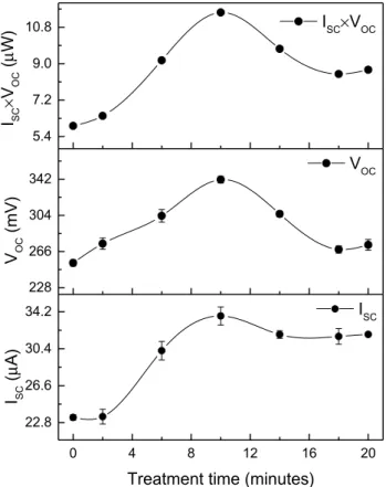
Figure 6 illustrates the variation of VOC and ISC with CdCl2 treatment time. The figure manifests both the superior ISC
and VOC values shown by all the films that underwent CdCl2 treatment (Table 3). Consequently, the highest ISC and VOC
values were shown by the film S-10. The observed supe-rior ISC values in the CdCl2-coated films potentially resulted from the improved gain size as observed in Fig. 5. Addition-ally, the highest ISC × VOC was seen for S-10, suggesting
bet-ter photoactivity of the film.
Improved electrical properties of CdCl2-treated films can be understood by looking into the structural changes which undergo as a result of the CdCl2 treatment. The presence of Cl−, resulting from CdCl
2 treatment has been identified to act as a fluxing agent that supports the grain growth process [38]. Also, the existence of large grains reduces the num-ber of grain boundaries as well as the scattering of charge carriers at the grain boundaries [38]. Therefore, a detailed explanation of the improvement of electrical properties is worth discussing here.
The mobility of the carriers in the films is affected by several factors including carrier concentration, annealing temperature, and defect complex formation. As the anneal-ing temperature was kept at constant (200 °C) throughout the work, the effect of annealing temperature can be ruled out from the discussion. The increment of the ISC value up
to 10 min of CdCl2 treatment time can be attributed from the increment of carrier concentration with the CdCl2 treatment time as shown in Table 3. The decrement in the ISC value
beyond the treatment time of 10 min can be due to the incre-ment of charged defect complexes with a growing diffusion concentration of Cl−. These defect centers surge the scat-tering rate for the carriers, reducing the mobility of carriers in the deposited films. Additionally, with the increment of Cl diffusion into CdS, vacant centers are filled with charge
0.0 0.5 1.0 1.5 2.0 2.5 3.0 3.5 4.0 100 002 101 110 103 TC Sample CdS CdS+CdCl2
carriers. Subsequently, these filled centers create potential barriers near the grain boundary which limits the mobility of carrier charges.
4.5 C–V measurement
Carrier concentration (ND) and Vfb were found from the
slope and the X-axis intercept of the linear fit of the Mott-Schottky equation [39]:
where e is the electron charge, A is the area, ε0 is the
per-mittivity in a vacuum and ε (= 8.5) is the dielectric constant [40]. The shape of the gradient of Mott-Schottky plot (1/
C2 vs. V) confirms all the grown films are n-type in nature.
Fig. 7 and Table 3 show the variation of Vfb of grown films
corresponding to the CdCl2 treatment time. These results facilitate visualization of the altering nature of the relative energy band edge position in the bandgap of the grown films corresponding to CdCl2 treatment time.
All the CdCl2-treated films showed significantly high Vfb
(with S-10 presence the highest), suggesting the existence of different energy band edge positions in the CdCl2-treated films compared to untreated. The relative band edge position (4) 1 C2 = 2 A𝜀𝜀0ND ( V− Vfb− kT e )
Fig. 5 Scanning electron microscope images of the grown CdS films; a CdCl2 treatment time 0 min, b CdCl2 treatment time 2 min, c CdCl2
treatment time 10 min and d CdCl2 treatment time 20 min
0 4 8 12 16 20 22.8 26.6 30.4 34.2 228 266 304 342 5.4 7.2 9.0 10.8 ISC I SC (µ A)
Treatment time (minutes)
VOC VOC (mV) ISC×VOC ISC × VOC (µ W)
Fig. 6 Open circuit voltage (VOC), short circuit current (ISC) and
variation, which is caused by the CdCl2 treatment, can be inter-preted in terms of variation of carrier concentration (Table 3) in the material or due to the presence of intermediate energy states. This suggests, as a result of the CdCl2 treatment, the concentration of donor atoms (ND) increases due to the
recrys-tallization process which in turn improves the (ND − NA), where
NA is the concentration of acceptors. Additionally, higher Vfb
produces greater electric field strength in the space charge region, improving the VOC value, hence the photoactivity of
the film. Additionally, the tunability of the relative energy band position of the material leads to the improvement of the electri-cal transport properties of the film, since the formation energy of VCd2+ causes band edge position to shift upwards.
5 Conclusions
CdCl2 treatment has significantly improved the electrical properties of CdCl2-treated films compared to untreated conventional CdS films. The enhancement of VOC in the
CdCl2-treated films can be concluded as a result of electri-cal passivation by CdCl2 and electrons states in the grain boundaries. The superior ISC value seen for CdCl2-treated films can be resulted from the improvement in the grain growth process due to diffusion of Cl− in to the CdS grains. The Eg value was found to vary from 2.33 to 2.41 eV along
with the CdCl2 treatment time with the highest Eg value
yielding at a dipping time of 10 min (S-10).
Furthermore, the occurrence of different relative energy band edge positions can also be a reason for the reported better electrical properties of CdCl2-treated CBD-CdS films in comparison to untreated CBD-CdS. Films dipped for 10 min in CdCl2 solution appeared to have the highest flat band potential and VOC.
Therefore, it can be concluded that the tunability of the relative band edge position, higher effective surface area due to higher roughness, recrystallization, and grain boundary passivation due to CdCl2 treatment has enhanced the elec-trical properties of the grown thin films. Best elecelec-trical and optical properties can be achieved with the treatment time of 10 min in CdCl2 solution.
Acknowledgements This work is financially supported by the Solar Edu-Training project of the Ministry of Science, Technology, and Research, Sri Lanka. Part of the research was performed at the Sensor Lab, Department of Information Engineering, Università Degli Studi Di Brescia, Brescia, Italy.
References
1. H. Moualkia, S. Hariech, M.S. Aida, Thin Solid Films 518, 1259– 1262 (2009). https ://doi.org/10.1016/j.tsf.2009.04.067
2. L. Wan, Z. Bai, Z. Hou, D. Wang, H. Sun, L. Xiong, Thin Solid Films 518, 6858–6865 (2010). https ://doi.org/10.1016/j. tsf.2010.07.011
3. C.S. Ferekides, D. Marinskiy, V. Viswanathan, B. Tetali, V. Pale-kis, P. Selvaraj, D.L. Morel, Thin Solid Films 361–362, 520–526 (2000). https ://doi.org/10.1016/S0040 -6090(99)00824 -X
4. G. Sasikala, R. Dhnasekaran, C. Subramanian, Thin Solid Films
302, 71–76 (1997). https ://doi.org/10.1016/S0040 -6090(96)09582 -X
Table 3 Variation of electrical and optical bandgap of the CdCl2-treated films
Best opto-electrical properties are presented in bold Dipping time
(minutes) ISC (µA) VOC (mV) ISC × VOC (µW) Eg (eV) Vfb (mV) ND (10
16 cm−3) 0 23.32 254.00 5.92 2.33 − 457.77 1.04 2 23.41 274.23 6.42 2.35 − 603.36 1.31 6 30.20 303.5 9.16 2.37 − 611.80 3.84 10 33.77 341.5 11.53 2.41 − 657.05 5.11 14 31.86 305.50 9.73 2.36 − 549.59 4.93 18 31.66 268.16 8.49 2.33 − 562.36 4.85 20 31.87 273.00 8.70 2.34 − 558.75 4.62 0 4 8 12 16 20 -700 -650 -600 -550 -500 -450 -400 Flatband potential Vfb (mV)
Treatment time (minutes)
Fig. 7 Flat band potential (Vfb) variation of the CdCl2-treated CdS
5. A. Gupta, V. Parikh, A.D. Compaan, Sol. Energy Mater. Sol. Cells 90, 2263–2271 (2006). https ://doi.org/10.1016/j.solma t.2006.02.029
6. H.C. Chou, A.R. Ohatgi, J. Electron. Mater. 23, 31 (1994). https ://doi.org/10.1007/BF026 51264
7. S.A. Al Kuhaimi, Vacuum 51(3), 349–355 (1998). https ://doi. org/10.1016/S0042 -207X(98)00112 -2
8. O. Savadogo, Chemically and electrochemically deposited thin films for solar energy materials. Sol. Energy Mater. Sol. Cells 52, 361–368 (1998). https ://doi.org/10.1016/S0927 -0248(97)00247 -X
9. E.X. Mathew, Sol. Energy Mater. Sol. Cells 76, 313–325 (2003).
https ://doi.org/10.1016/S0927 -0248(01)00090 -3
10. W.G.C. Kumarage, R.P. Wijesundera, V.A. Seneviratne, C.P. Jay-alath, B.S. Dassanayake, J. Phys. D. Appl. Phys. 49, 95109 (2016).
https ://doi.org/10.1088/0022-3727/49/9/09510 9
11. W.G.C. Kumarage, L.B.D.R.P. Wijesundara, V.A. Seneviratne, C.P. Jayalath, B.S. Dassanayake, Procedia Eng. 139, 64–68 (2016). https ://doi.org/10.1016/j.proen g.2015.09.215
12. W.G.C. Kumarage, R.P. Wijesundera, V.A. Seneviratne, C.P. Jay-alath, T. Varga, M.I. Nandasiri, B.S. Dassanayake, Mater. Chem. Phys. 200, 1–8 (2017). https ://doi.org/10.1016/j.match emphy s.2017.07.052
13. W.G.C. Kumarage, L.B.D.R.P. Wijesundara, V.A. Seneviratne, C.P. Jayalath, B.S. Dassanayake, Semicond. Sci. Technol. 32, 045014 (2017). https ://doi.org/10.1088/1361-6641/aa5ee 3
14. F. Liu, Y. Lai, J. Liu, B. Wang, S. Kuang, Z. Zhang, J. Li, Y. Liu, J. Alloy. Compd. 493, 305–308 (2010). https ://doi.org/10.1016/j. jallc om.2009.12.088
15. M. Tsuji, T. Aramoto, H. Ohyama, T. Hibino, K. Omura, Jpn. J. Appl. Phys. 39, 3902–3906 (2000). https ://doi.org/10.1143/ JJAP.39.3902
16. I.M. Dharmadasa, Coatings 4, 282–307 (2014). https ://doi. org/10.3390/coati ngs40 20282
17. J. Salinger, J. Acta Polytechnica 46, 25–27 (2006)
18. M.J. Kim, J.J. Lee, S.H. Lee, S.H. Sohn, Solar Energy Mater. Solar Cells 109, 209–214 (2013). https ://doi.org/10.1016/j.solma t.2012.11.012
19. D.B. Laks, C.G. Van de Walle, G.F. Neumark, S.T. Pantelides, Phys. Rev. Lett. 66, 648–651 (1991)
20. M.A. Islam, M.S. Hossain, M.M. Aliyu, M.R. Karim, T. Razykov, K. Sopian, N. Amin, Thin Solid Films 546, 367–374 (2013). https ://doi.org/10.1016/j.tsf.2013.04.067
21. J. Lee, Curr. Appl. Phys. 11(1), 103–108 (2011). https ://doi. org/10.1016/j.cap.2010.11.099
22. A. Rios-Flores, J.L. Peña, V. Peña, O. Ares, R. Castro-Rodríguez, A. Bosio, Sol. Energy 84(6), 1020–1026 (2010). https ://doi.org/10.1016/j.solen er.2010.03.010
23. W.G.C. Kumarage, R.P. Wijesundera, V.A. Seneviratne, C.P. Jay-alath, T. Varga, B.S. Dassanayake, Appl. Phys. A 124, 494 (2018).
https ://doi.org/10.1007/s0033 9-018-1910-0
24. K.K.M.B.B. Adikaram, W.G.C. Kumarage, T. Varga, B.S. Das-sanayake, J. Electron. Mater. 48(7), 4424–4431 (2019). https :// doi.org/10.1007/s1166 4-019-07215 -5
25. W.G.C. Kumarage, R.P. Wijesundera, V.A. Seneviratne, C.P. Jayalath, N. Kaur, E. Comini, B.S. Dassanayake, J. Photochem. Photobiol. A 367, 171–177 (2018). https ://doi.org/10.1016/j.jphot ochem .2018.08.029
26. A. Oliva-Avilés, R. Patiño, A. Oliva, Appl. Surf. Sci. 256, 6090– 6095 (2010). https ://doi.org/10.1016/j.apsus c.2010.03.125
27. A. Mukherjee, P. Ghosh, A.A. Aboud, P. Mitra, Mater. Chem. Phys. 184, 101–109 (2016). https ://doi.org/10.1016/j.match emphy s.2016.09.030
28. A.I. Oliva, O.S. Canto, R.C. Rodrigues, P. Quintana, Thin Solid Films 391(1), 28–35 (2001). https ://doi.org/10.1016/S0040 -6090(01)00830 -6
29. A. Kariper, E. Güneri, F. Gödethe, C. Gümüs, T. Özpozan, Mater. Chem. Phys. 129, 183–188 (2011). https ://doi.org/10.1016/j.match emphy s.2011.03.070
30. S.A. Ringel, A.W. Smith, M.H. MacDougal, A. Rohatgi, J. Appl. Phys. 70(2), 881 (1991). https ://doi.org/10.1063/1.34965 2
31. A. Luque, S. Hegedus, Handbook of photovoltaic science and
engineering (John Wiley & Sons, Chichester, 2011)
32. S. Du, Y. Li, Adv. Mater. Sci. Eng. 2015, 8 (2015). https ://doi. org/10.1155/2015/96958 0
33. V. Bilgin, S. Kose, F. Atay, I. Akyuz, J. Mater. Sci. 40, 1909–1915 (2005). https ://doi.org/10.1007/s1085 3-005-1210-x
34. P.K.K. Kumarasinghe, A. Dissanayake, B.M.K. Pemasiri, B.S. Dassanayake, Mat. Sci. Semicon. Proc. 58, 51–60 (2017). https :// doi.org/10.1016/j.mssp.2016.11.028
35. P.K.K. Kumarasinghe, A. Dissanayake, B.M.K. Pemasiri, B.S. Dassanayake, Mater. Res. Bull. 96, 188–195 (2017). https ://doi. org/10.1016/j.mater resbu ll.2017.04.026
36. H.R. Moutinho, R.G. Dhere, M.M. Al-Jassim, D.H. Levi, L.L. Kazmerski, J. Vac. Sci. Technol. A17, 1793 (1999). https ://doi. org/10.1116/1.58189 2
37. A. Nawaz, Z. Rabeel, N.A. Shah, World Appl. Sci. J. 31(8), 1522– 1530 (2014). https ://doi.org/10.5829/idosi .wasj.2014.31.08.621
38. P.K.K. Kumarasinghe, A. Dissanayake, B.M.K. Pemasiri, B.S. Dassanayake, J. Mater. Sci.: Mater. Electron. 28, 276–283 (2017).
https ://doi.org/10.1007/s1085 4-016-5521-2
39. M. Akif, S. Aliyev, M. El-Rouby, Int. J. Thin Film Sci. Technol.
2, 195–2005 (2013). https ://doi.org/10.12785 /ijtfs t/02030 5
40. W.G.C. Kumarage, R.P. Wijesundera, N. Kaur, D. Zappa, V.A. Seneviratne, C.P. Jayalath, B.S. Dassanayake, Int. J. Electroact. Mater. 7, 1–6 (2019)
Publisher’s Note Springer Nature remains neutral with regard to jurisdictional claims in published maps and institutional affiliations.