Scuola di Scienze
Corso di Laurea Magistrale in Fisica
Investigation of dangling bounds in Al
2O
3passivated Si surface using electron
paramagnetic resonance (EPR)
Relatore:
Prof. Anna Cavallini Correlatore:
Dott. Saskia K¨uhnhold
Presentata da: Valentina Roberti
Sessione III
Nel presente lavoro di tesi magistrale, svolto presso l’istituto Fraunhofer-ISE, Fraunhofer Institute for Solar Energy Systems, a Friburgo in Brisgovia, sono stati depositati e caratterizzati sottili film di ossido di alluminio, Al2O3, (di spessore compreso tra 3-30 nm) su un substrato di FZ-Si, silicio cresciuto con il metodo float zone, drogato p. La deposizione è avvenuta mediante plasma ALD (plasma enhanced
Atomic Layer Depostion). La tecnica spettroscopica EPR (Electron Paramagnetic Resonance) è stata
utilizzata per studiare l’interfaccia Si/Al2O3, con e senza la presenza di un sottile strato di ossido di silicio, SiOx, tra di essi, con lo scopo di scoprire l’origine della formazione di densità di carica negativa Qf all’interfaccia Si/Al2O3: tale carica negativa induce una passivazione per effetto di campo ed è quindi la ragione per cui il dielettrico Al2O3 risulta essere un ottimo materiale passivante.
In tale studio, si è deciso di variare alcuni parametri, come lo spessore dello strato di Al2O3, lo spessore dello strato intermedio di ossido di silicio, depositato mediante ossidazione termica (dry
thermal oxidation), e la superficie del substrato di silicio. Oggetto di studio è stato inoltre l’effetto di
trattamenti termici, come l’annealing, sui campioni di Si/Al2O3 e Si/SiOx/Al2O3.
Sono stati realizzati cinque differenti gruppi di campioni: per ciascuno di essi sono state impiegate varie tecniche di caratterizzazione dei materiali, come la QSSPC (Quasi Steady State
Photoconuctance), per la misura della vita media dei portatori minoritari, e la tecnica di spettroscopia
ottica SE (spettroscopic ellipsometry). Per quattro di tali gruppi è stato utilizzato come substrato uno strato di FZ-Si drogato p, di spessore 50 µm, e con una resistività di 100 Ohm·cm; per il quinto gruppo di campioni, invece, lo spessore il substrato FZ-Si ha uno spessore 250 µm e una resistività di 100 Ohm·cm.
Per ogni gruppo di campioni sono stati riportati gli spettri EPR ottenuti ed i rispettivi fit, da cui è stato possibile risalire ai fattori giromagnetici di spin g, i quali sono stati riportati in tabelle con le loro possibili attribuzioni.
E’ stato dimostrato che la presenza di uno strato di ossido di silicio tra il substrato di silicio e lo strato di ossido di alluminio risulta essere fondamentale per la formazione di densità di carica negativa all’interfaccia: aumentando lo spessore dello strato di SiOx (nel range 1-30 nm) si assiste ad una diminuzione di carica negativa Qf. Infatti, l’ossido di silicio si comporta come una barriera riducendo l’iniezione di portatori dal substrato di silico agli stati difettivi all’interfaccia SiOx/Al2O3. In questo studio, l’effetto sopradescritto è stato dimostrato utilizzando la tecnica COCOS
(Corona-Oxide-Semiconductor Characterization).
Inoltre, è stato dimostrato, sempre utilizzando la tecnica COCOS, che per i campioni sottoposti ad
annealing, la denistà di carica negativa Qf tende ad aumentare, così come il tempo di vita media dei
portatori minoritari.
Analizzando gli spettri EPR, è stato possibile concludere che all’interfaccia Si/Al2O3 sono presenti difetti, denominati , caratteristici dell’interfaccia Si/SiOx. Le nostre osservazioni, dunque, sono
coerenti con la formazione di uno strato di ossido di silicio tra Si e Al2O3.
Dallo studio degli spettri EPR del gruppo 1, è stato possibile indentificare tre principali stati difettivi: un
centro isotropo, un centro E’ e un centro anisotropo (di tipo ). Una volta sottoposti i campioni ad
annealing, gli spettri EPR non hanno rivelato la presenza di stati difettivi.
In tale lavoro, infine, è stata studiata la dipendenza angolare del fattore giromagnetico di spin, variando l’angolo tra il campo magnetico B e la normale all’interfaccia (100) in un range compreso tra 0°-90°.
Abstract
In the present thesis, performed at the Fraunhofer Institute for Solar Energy Systems, thin layers of aluminium oxide (Al2O3) were characterized and deposited on a silicon substrate (FZ-Si, p doped). Al2O3 deposition was performed using plasma enhanced Atomic Layer Deposition. Electron Paramagnetic Resonance (EPR) has been used to investigate the interface between Si and the high-k dielectric Al2O3, with or without the presence of a thermal grown SiOx layer. The aim of this work is trying to understand the origin of the fixed negative charge density Qf, that induces field effect passivation, formed at the SiO2/Al2O3 interface. In our study several parameters were varied: the thickness of the Al2O3 layer, the interlayer SiOx thickness, the thickness and the surface of the Si substrate. Also the effect of treatments (annealing) on Si/Al2O3 and Si/SiOx/Al2O3 stacks were considered.
Five different groups of samples have been under study: for the first four groups, the starting substrates was p FZ-Si, 50 µm thick and with a resistivity of 100 Ohm·cm; the starting substrate for group 5 is p-FZ Si, with a thickness of 250 µm and a resistivity of 100 Ohm·cm. For each group characterization techniques were used: the optical spectroscopy technique SE (spettroscopic
ellipsometry), for thickness measurements and the QSSPC (Quasi Steady State Photoconuctance), for
lifetime measurements. In addition, for each group of samples, EPR spectra and fits were reported. From these fits, it was possible to obtain the electron spin g-factors: g-factor values and their possible attributions were reported in tables. It has been demonstated that the presence of a SiOx interlayer between Si and Al2O3 plays a key role in the origin of the negative charge formation and in the interface defect density: an increase in the SiOx interlayer thickness over the range 1-30 nm gives rise to a decrease in negative Qf. As a matter of fact, SiOx acts as a barrier, reducing charge injection from the Si substrate into defect states at the SiOx/Al2O3 interface. In our study this effect has been demonstrated using the COCOS technique (Corona-Oxide-Semiconductor Characterization)
layer thickness.
Our observations, using EPR spectroscopy, are in line with the formation of an interfacial SiOx layer. Analysing the spectra of group 1 (Si/Al2O3), it was possible to identify an isotropic center, an E’-like
defect and an anisotropic center P !-like. The E’-like defects are associated with the SiOx interface.
After an annealing step, EPR did not reveal the presence of any defect states. Finally, in our work we studied the angular dependence of the g values varying the angle between B and the (100) interface normal in a range 0°-90°. In all the spectra we found the presence of signals due to the trigonal
Table of contents
Table of contents ... I
1 Introduction ... 5
2 Objectives of this Thesis ... 5
2.1 Structure of this work ... 8
3 Photovoltaic technologies ... 9
3.1 Introduction ... 9
3.2 The photovoltaic effect: history ... 11
3.3 Solar radiation ... 13
3.4 Solar cell short description ... 14
3.5 Standard Si solar cell ... 17
3.6 Simplest description of photovoltaic devices ... 18
3.7 Figures of merit ... 20
3.8 Material properties... 21
3.9 The PERC concept ... 22
4 Fundamental properties of semiconductors ... 24
4.1 Silicon fundamental properties ... 25
4.2 Dopant atoms and energy levels ... 25
4.3 Carrier concentration ... 26
4.3.1 Intrinsic concentration ... 28
4.3.2 Charge neutrality ... 28
4.4 Fermi energy level ... 29
4.4.1 Quasi Fermi energy levels ... 31
Table of contents
4.5.1 Silicon Dangling Bonds ... 33
5 Recombination mechanisms ... 34
5.1 Radiative recombination ... 35
5.2 Auger recombination ... 37
5.3 Recombination mediated by defects ... 38
5.4 Surface recombination ... 41
5.5 Emitter recombination ... 43
5.6 Effective lifetime ... 43
6 Surface passivation ... 44
6.1 Chemical passivation ... 45
6.2 Field effect passivation ... 46
6.3 A short review of surface passivation materials ... 47
7 Crystal lattices... 49
7.1 Primitive lattice cell ... 50
7.2 Types of lattice ... 51
7.3 Coordination number ... 52
7.4 Reciprocal lattice ... 52
7.5 Lattice planes and Miller indices ... 55
7.6 Silicon crystal structure ... 56
7.6.1 Silicon wafer orientation ... 57
8 Characterization techniques ... 58
8.1 Quasi-Steady State Photo Conductance (QSSPC) ... 58
8.2 Spectral ellipsometry ... 61
8.3 Electron paramagnetic resonance (EPR) ... 62
9 EPR: theoretical aspects ... 63
9.1 Historical overview... 63
9.2 Orbital magnetic dipole and Larmor precession ... 68
9.4 Electron-nuclear hyperfine interaction ... 78 9.5 g-factor ... 82 10 EPR spectrometer ... 85 10.1 Source... 86 10.2 EPR cavity ... 87 10.3 Magnetic field ... 88 10.4 Signal channel ... 89
10.5 Magnetic field controller ... 89
10.6 Spectrum ... 90
11 Oxidation and Deposition techniques ... 91
11.1 Atomic Layer Deposition (ALD) ... 91
11.2 Dry thermal oxidation ... 94
12 Experimental plan and results ... 97
12.1 Introduction ... 97
12.2 EPR experiments ... 97
13 Conclusion ... 138
14 Appendix ... 140
14.1 Corona-Oxide-Semiconductor Characterization ... 140
14.2 Experimental set up: pictures... 142
1
Introduction
In order to reduce the costs of photovoltaic energy, the introduction of a passivation layer on the rear of the crystalline-silicon solar cells seems to be a successful strategy. This layer allows the increase of the light trapping, the decrease of the surface recombination losses and higher conver-sion efficiency. Also the use of thinner wafers becomes possible. In 2006, aluminum oxide (Al2O3) nanolayers were found to be a new solution for the passivation of p- and n- type crystalline Si surfaces [2]. Fixed negative charges induce an accumulation layer at the p-type silicon interface that yields to a very effective field-effect passivation.
2
Objectives of this Thesis
In this work, Electron paramagnetic resonance, EPR, has been used to investigate the interface between Si and the high-k dielectric Al2O3, with or without the presence of a thermal grown SiOx layer. We also tried to understand the origin of the negative charge formation at the SiO2/Al2O3 interface. In this section the main properties of the dielectric Al2O3 are reported.
Al2O3 can deliver excellent passivation qualities on Si substrates [1]. Several Al2O3 deposition techniques has been established in the last few years like Plasma Enhanced Chemical vapor Deposition (PECVD) [2], plasma enhanced and thermal Atomic Layer Deposition [3], plasma enhanced and thermal ALD [4], [5] have very low surface recombination velocities
6 Objectives of this Thesis
At the present time high efficiencies have been realized by the implementation of ultrathin Al2O3 films in laboratory and industrial solar cells.
Why is Al2O3 a very good surface passivation material?
The passivation properties of Al2O3 were already reported by Hezel and Jaeger in 1989 [8]. Al2O3 features a good field effect passivation. Due to the presence of a high density of inherent negative charges at the interface, the electric field enhanced by negative charge accumulation at the p-type Si/Al2O3 interface deflects minority charge carriers.
In addition to the field effect passivation, the Al2O3 also provides good chemical passivation of the dangling bongs, reducing interface defect density [2].
As far as optical properties are concerned, with a low refractive index of 1.65 Al2O3 is well suited to improve the optical quality at the front or at the back of the solar [3] because of low absorption in the visible part of solar spectrum. It acts as a back surface reflector for the long wavelength spectra of light to increase the light trapping inside the solar cells.
Al2O3 shows also a low dependence on injection levels [9]. Even at low illumination conditions, the solar cells passivation using aluminum oxide provides a good passivation quality.
Moreover Al2O3 has a high thermal stability [10]. In fact the passivation quality of the dielectric material should be thermally stable in order to sustain high temperature processes used in solar cell production.
During deposition processes an interfacial SiOx layer is commonly formed between the Al2O3 film and the c-Si substrate [3]. This thin SiOx layer can be formed during the Al2O3 deposition process but also during the post deposition annealing. Hoex et al. found an interfacial SiOx layer of ~ 1.5 nm using High resolution TEM image[3].
Figure 2-1: High resolution TEM image showing a 20 nm thick Al2O3 film on c-Si prepared by plasma-assisted atomic layer deposition after 30 min annealing at 425°C in a N2 environment [3]
This could be a result of the deposition process, possibly from the exposure of the substrate to the O2 plasma in the first ALD cycles [3].
The microscopic origin of defect states in the Si/Al2O3 system that lead to fixed negative charges Qf has not been clearly understood so far. It is known that the origin of the charge traps are point defects, such as vacancies and interstitials [11]. Al vacancy !" and O interstitial $% produce levels in the Al2O3 bandgap below midgap [12]. These both defects are in fact likely candidates to trap negative fixed charge. When the negative charge is related to these two defects a slightly oxygen-rich structure in proximity of the Si interface would be expected. Another issue is the role of Charging of Defect states. Electron injection in the conduction band and tunneling from the dielec-tric into the substrate can change the charge state of an ionized defect. As far as Si/Al2O3 system is related, there are some indications that charge injection from Si into Al2O3 could play an im-portant role in the negative charge formation. For annealed Al2O3 samples, the fixed charged density was observed to increase on the Al2O3 surface. It has been demonstrate also that an increase in the SiO2 interlayer thickness over the range 1-30 nm gave rise to a decrease in nega-tive Qf [11, 13].
8 Objectives of this Thesis
2.1
Structure of this work
In Chapter 3, some basic concepts of photovoltaic devices are discussed. After an introduction about photovoltaic technologies, a short description of a standard Si solar cell is given. The most significant material properties, fundamental to achive high efficiency solar cells, are summarized. Finally, a short introduction of the PERC solar cells is given: they are based of the concept of passivated emitter and rear cells.
In Chapter 4, the fundamental properties of semiconductors are reported: Silicon fundamental properties, dopant atoms and energy levels, carrier concentration, Fermi energy level and the main defects in semiconductor materials.
In Chapter 5, the main recombination mechanisms in semiconductors are discussed: radiative recombination, Auger recombination, recombination mediated by defects, surface recombination and emitter recombination.
In Chapter 6, the two main ways to achieve surface passivation are reported: chemical passivation and field effect passivation. Finally, a short review of surface passivation materials is given.
In Chapter 7, a short description of crystal lattices is given: the silicon crystal structure is described. In Chapter 8, the main characterization techniques used in this work are reported: Quasi-Steady State Photoconductance (QSSPC), Spectral Ellipsometry and Electron Paramagnetic Resonance (EPR).
In Chapter 9, the main theoretical aspects of EPR are discussed. After a hystorical overview, orbital magnetic dipole, Larmor precession, spin-orbit interaction and electron-nuclear hyperfine interac-tion are described.
In Chapter 10, an analysis of the four essential components of an EPR spectrometer is carried out: Source, EPR cavity, magnetic field, signal channel, magnetic field controller and spectrum.
In Chapter 11, the deposition and oxidation techniques used in this work are discussed: Atomic Layer Deposition (ALD) and Dry Thermal Oxidation.
In Chapter 12, the detailed plan, methodology and results obtained are discussed for the five main experiments performed using EPR. The aim of the experiments is explained and for each group the detailed experimental process flow is described. The EPR sprectra are reported and compared. The final sections of each group of experiments discuss the analysis and conclusion of the experi-mental findings.
Chapter 13 gives the overall summary of the thesis work and the main conclusions.
Chapter 14 is the Appendix section: it includes also additional figures to supplement the information
in the main work.
3
Photovoltaic technologies
3.1
Introduction
Infrared active gases, such as water vapor (H2O), carbon dioxide (CO2) and ozone (O3), absorb thermal infrared radiation emitted by the Earth’s atmosphere and surface. This mechanism warms the atmosphere that emits infrared radiation: a significant portion of this energy warms the surface and the lower atmosphere. This phenomenon is called “greenhouse effect” and consituets at the present time the main origin of global warming. The amplitude of the dramatic consequences of this global warming on human, as well as vegetal and animal life is difficult to predict. Some predictions however are based largely on computer models that simulate fundamental geophysical
process-10 Photovoltaic technologies
es.Modern civilization has a big need of energy, which is mainly provided by fussil fuels. As world-wide energy demand increases, conventional fossil fuels will be exhausted within the next century (the resources of fossil fuels will probably not last longer than 50 years). The side effect of using fossil fuels is the release of greenhouse gases such as carbon dioxide to the environment. The transition from fossil fuel to renewable energy sources is therefore necessary. Renewable electricity or power from wind, water and sun will play a main role in a safe and stable energy transition [1]. The major candidate for obtaining energy from the sun is the solar cell[1]. Solar Photovoltaic systems provide clean energy from small scale residential to large industrial applications. Recently researches of low-cost flat-panel solar panels, thin-film devices and many innovative concepts have increased. The global solar photovoltaic market has shown a significant growth due to the use of this source of solar power generation.
New photovoltaic installation have been made in the year 2010 and in 2011, a total of 69 GWp of PV panels were installed worldwide with a capacity to generate some 85TWh of electricity annually. PV technology is become more and more important and constitutes a competitive solution for power generation with high effriciency (obtained in laboratory) of above 24 %.
Figure 3-1: Worl PV Cell/Module Production from 1990 to 2007 (data source: PV News[Pvn 2008], Photon Interna-tional [Pho 2008])
To reduce the total cost related to solar technology must be reduced. One way to achieve this goal is the reduction of wafer thickness. A new generation of thinner solar cell has begun. However, increasing the surface to volume ratio electrical losses occur due to surface recombination. This problem causes losses in electrical efficiency in the solar cells. To minimize these losses, due mostly to the presence of dangling bonds at the crystal surface, thin dielectric layers are applied to reduce surface recombination. Standard passivation layers are Silicon dioxide (SiO2), Silicon Nitride (SiNx) and hydrogenated amorphous Silicon (a-Si:H). These passivation layers however are found not to be suitable during all cases of application limitin solar cell efficiency.
New technologies and new passivation layer are therefore required. One such technology coul be the passivated emitter and rear solar cell (PERC): the cell is passivated on both emitter and rear side in order to reduce recombination at the interface. An alternative passivation layer colud be Aluminum Oxide (Al2O3): it has suitable properties such as a refractive index of about 1.65 with low absorption in the visible region of the solar spectrum and low density of interface states leading to high quality of chemical passivation.
3.2
The photovoltaic effect: history
Solar cells operate by converting sunlight directly into electricity using the electronic properties of a class of material known as semiconductors. A semiconductor material or device is said to be “photovoltaic” when exposure of the material to light that can be absorbed by the material is able to transform the energy of the light photons into electrical energy in the form of a current and voltage. The number of materials that are able to exhibit photovoltaic characteristic is large but the number of such materials or devices that are able to make the transformation of solar radiation to electrical energy with high efficiency , of the order of 20%, at low cost and with stability is not large [3].
12 Photovoltaic technologies
The photovoltaic effect was discovered by Becquerel, a French experi-mental physicist, while experimenting with an electrolytic cell made up of two metal electrodes in 1839 [3]. Willoughby Smith discovered the photo-conductivity of selenium in 1873. In 1904 Hallwachs discovered that a combination of copper and cuprous oxide was photosensitive. Solar efficiencies of about 1% characterized selenium and copper oxide cell by about 1914.[3] In this year Einstein published his paper on the photoelec-tric effect.
Millikan provided experimental proof of the photoelectric effect in 1916. Two year later a Polish scientist named Czochralski developed a way to grow single-crystal silicon. In 1954 the PV effect in Cd was reported; primary work was performed by Rappaport, Loferski and Jenny at RCA. Bell Labs researchers Pearson, Chapin, and Fuller reported their discovery of 4.5% efficient silicon solar cells; this was raised to 6% only a few months later (by a work team including Mort Prince). Chapin, Fuller, Pearson (AT&T) submitted their results to the Journal of Applied Physics. AT&T demonstrat-ed solar cells in Murray Hill, New Jersey, then at the National Academy of Science Meeting in Washington, DC. The year 1954 also dates the announcement of the first all-thin-film cell composed of a Cu&S/ CdS junction with an efficiency of 6%, later increased to over 9%. One year later, Western Electric began to sell commercial licenses for silicon PV technologies; early successful products included PV-powered dollar bill changers and devices that decoded computer punch cards and tape. Bell System's demonstration of the type P rural carrier system began in Americus, Georgia.[1, 3] In 1964 Peter Glaser, A.D. Little, conceived the idea of a satellite solar power station. Tyco Labs developed the edge-defined, film-fed growth (EFG) process, first to grow crystal sap-phire ribbons and then silicon. To date, solar cells have been made out of many other semiconduc-tors, using various device configurations and employing single crystal, polycrystal, and amorphous thin-film structures [1].
Figure 3-2: Antoine-Henri Becquerel
3.3
Solar radiation
Nuclear fusion reaction is the origin of the radiative energy output from the sun. In every second, about 6x10¹¹ kg of H' is converted to He, that corresponds to a net mass loss of about 4x10³ kg , that is converted through the Einstein relation:
( = )*' (3.1)
to 4x10²⁰ kg . This energy is emitted primarily as electromagnetic radiation in the ultraviolet to infrared and radio spectral ranges. Now the total mass of the sun is about 2x1030 kg. The sunlight is attenuated by the atmosphere when it reaches the earth’s surface: this is mainly due to water-vapor absorption in the infrared, ozone absorption in the ultraviolet, and scattering by airborne dust and aerosols. Air mass quantifies the degree to which the atmosphere affects the sunlight received at the earth’s surface. The air mass number (AM) is the secant of the angle between the sun and the zenith and it measures the atmospheric path length relative to the minimum path length when the sun is directly overhead. The AM0 spectrum represents the solar spectra outside the earth’s at-mosphere and the AM1 spectrum represents the sunlight at the earth’s surface when the sun is at zenith and the incident power is about 925 W/m2 .The AM2 spectrum is the spectrum for ȟ =
14 Photovoltaic technologies
Figure 3-3: Solar spectrum at different air-mass conditions [1]
Figure 3-3 shows the solar spectrums at various AM conditions. The upper curve is the AM0 condi-tion. This spectrum is the relevant one for satellite and space-vehicle applicacondi-tion. For terrestrial applications, the AM1.5 conditions, with sun at 45° above the horizon, represent an energy-weighted average. Because each photon produces an electron-hole pair, the solar power has to be converted in photon flux [1]. To convert the wavelength to photon energy we have to use this expression is used:
+ =, =* ℎ,(5V) µm 1.24
(3.2)
The total power for AM1.5 is 844 W/m'[1].
3.4
Solar cell short description
Semiconductors are crystalline materials whose outer shell atomic levels exhibit an energy band structure.This band structure is due to the close, periodic arrangement of the atoms in the crystal which causes an overlapping of the electron wavefunctions. The so called Valence Band (VB) is the
highest occupied energy level at zero point temperature. The Conduction Band (CB) is the next unoccupied energy level at the zero point. There is an energy gap between valence and conduc-tion bands of the order of ∼ 1eV. Figure (3.4) schematically illustrates this basic structure consist-ing of a valence band,a forbidden energy gap and a conduction band. The band configuration for conductors and insulators is also shown for comparison. At zero temperature all allowed energy states in the valence band are completely occupied and all allowed energy states in the conduction band are completely empty. As the temperature increases, the number of thermally excited elec-trons across the forbidden band gap increases. The Fermi energy level corresponds to the energy of the highest occupied state in the system.
The probability of occupation of allowed energy states of any given energy E in thermal equilibrium is described by the Fermi-Dirac distribution [4]:
<(() = 1
1 + exp ?( − (A
BDE F
(3.3)
where T is the temperature in Kelvin and BD is the Boltzmann’s constant and (A is the Fermi energy level.
Figure (3.4) schematically illustrates this basic structure consisting of a valence band,a forbidden energy gap and a conduction band. The band configuration for conductors and insulators is also shown for comparison.
16 Photovoltaic technologies
Figure 3-4: Energy band structure of conductors, insulators and semiconductors
When a photon with energy larger than the Band Gap strikes an electron in the silicon crystal lattice, the energy gets absorbed and the electron is ejected from its state in the Valence Band to a free excited state in the Conduction State and it can contribute to the electrical conduction.
A solar cell works on the principle of the ‘’ photovoltaic effect’’. When a solar cell is exposed to light, the photon energy is absorbed by the semiconducting material: electron-hole pairs are created, resulting in the generation of free charge carriers. These charge carriers are separated across a space charge region (p-n junction). At the p-n junction the potential energy of the n-type and p-type substates become identical.The p-n junction permits the partial separation of charges, allowing electrons to diffuse to emitter and holes to diffuse to the bulk to reach the junction terminals. Near the p-n junction the electrons diffuse into the vacant holes in the p material causing a depletion zone, the space charge region (SCR)This depletion zone acts like an insulator preventing other free electrons in the n-type silicon and holes in the p-type silicon from combining[1, 4].This forms an electric field across the p-n junction, opposing the diffusion force.Finally, the movement of these charges through an external circuit creates electrical generation. A potential difference is built by the charge accumulation at the emitter (n-region) and bulk (p-region) terminals. The charge con-centration at these terminals develops a photocurrent which flows in the opposite direction respect to the diffusion current. An external load is connected between the front and the back contacts of
the solar cell. When the overall magnitude of photocurrent is bigger than the diffusion current a current flow is extracted.
The crystalline silicon (c-Si) solar cell, which dominates the PV market at present, has a simple structure, and provides a good example of a typical solar cell structure. In the next chapter a standard Si solar cell is described.
3.5
Standard Si solar cell
The structure of a silicon solar cell is composed of a bulk substrate (usually p-type semiconductor) and an emitter (n-type semiconductor) forming a p-n junction.
Figure 3-5: Illustratiuon of a standard solar-cell. The base and the emitter form a p-n junction. Electrons and holes are separated by an electric field and a potential difference is created
At the front surface above the emitter a thin dielectric layer is usually employed as an Anti-ReflectionCoating (ARC).This Anti-Reflection Coating is used to reduce reflection losses at the front surface.
18 Photovoltaic technologies
ARC consists of a thin dielectric layer, with a certain thickness so that light reflection gets disabled due to destructive interference. Of course this interference condition is true only for a certain wavelength. The antireflection coating is usually optimized for l=600 nm.
Figure 3-6: ARC consist of a dielectric layer, with a specially chosen thickness so that interference effects in the coating cause the wave reflected from the anti-reflection coating top surface to be out of phase with the wave reflected from the semiconductor surfaces. These out-of-phase reflected waves destructively interfere with one another, resulting in zero net reflected energy
3.6
Simplest description of photovoltaic devices
Figure 3-7: Simple equivalent circuit for a photovoltaic cell, with a current generator with total light current IG, a diode with total dark current IJ, a series resistance RK, and a parallel resistance RL [3]
We can consider an “ideal device” with MN = 0 and MO = ∞. The current density J flowing in the device in the presence of photo excitation can be expressed with this equation:
Q = QTUexp X[BE\ − 1] − QYZ ^ (3.4)
The first term on the right, QT_exp ?`a
bfgF − 1h, is the forward current driven by the voltage Z
and the second term, Q^ is the reverse current that is associated with photoexcitation. QT is also called “reverse saturation current” of the diode. A is the “ideality factor” that has a value depending on the mechanism of the junction transport. If the voltage is 0 we have the short-circuit condition and there is zero current in the dark.
In the light we have:
Qij = −Q^ (3.5)
The short circuit current is controlled only by the photoinduced current generation and recombina-tion processes. If the total current under illuminarecombina-tion is zero (open-circuit condirecombina-tion) we obtain:
ϕOC= XAkTq \ ln UXJJL
0\ +1] (3.6)
We can see that the open-circuit voltage is controlled by the current generation and recombination processes but also by the nature of the junction transport currents.
The relation between Qij and Zzj is given by:
20 Photovoltaic technologies
3.7
Figures of merit
The efficiency of a solar cell is maximal when the product of the current density Q and the voltage Z is a maximal. The efficiency { can be expressed in this way:
{ =||} = Q}Z} | = QNZ | (3.8)
where | is the total radiation power incident on the cell and is called the fill factor: it is the measure of the “sqareness” of the light − curve.
Figure 3-8: I-V characteristic of a solar cell during light and dark condition[3]
and ! are respectively the values of current density and voltage at the condition correspond-ing to maximum power.
The definition of the fill factor FF is given by the following equation:
with:
! = !%$ − (&')*/+)ln [(+! /&')*) + 1] (3.10)
Once a value for ! has been obtained, the value of and the maximum power . = ! can be obtained.
3.8
Material properties
We can summarize the most significant material properties that are fundamental to achive high efficiency solar cells.
The band gap of the absorbing material should be small enough to allow absorption of an appre-ciable portion of the solar spectrum but at the same time large enough to minimize the reverse saturation junction current density. The diffusion length of minority carriers 0 23 must be as large as possible so that carriers excited by light will be able to diffuse to the junction and be collected before they recombine with carriers of the opposite sign.
0 23 = (4 235 23)6 (3.11)
4 23 ist he diffusion constant and 5 23 ist he lifetime of minority carriers
Using the Einstein relation:
43 73 = 48 78 = ')* + (3.12)
22 Photovoltaic technologies
Equation (3.9) becomes:
0 23 = 9:')+ ; (75)* 23< >/6
(3.13)
where 7 23 and ') are the mobility for minority carriers and the Boltzmann constant respectively. It is desired, therefore, to have a material in which the minority carriers have large mobility and lifetime.
The junction structure and composition are also important because they determine the magnitude of the junction transport current density ?and of the ideality factor A. To produce junctions with as low junction current as possible the formation of the semiconductor junction must be carefully controlled [3].
3.9
The PERC concept
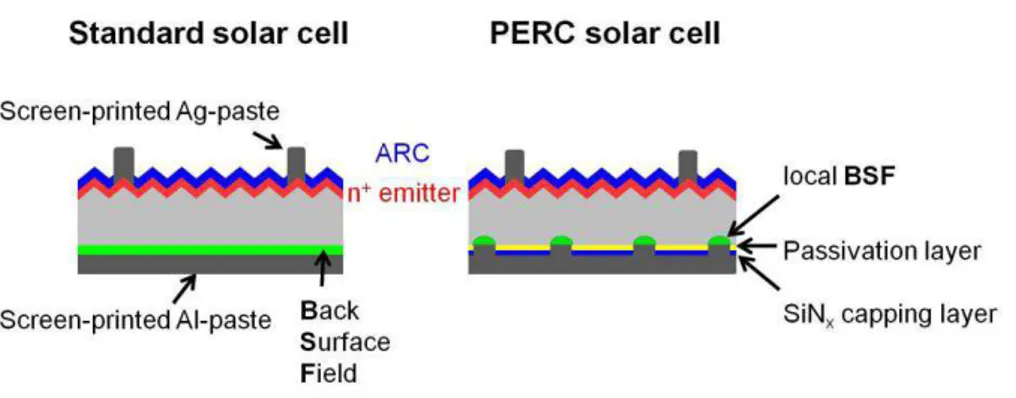
In PERC solar cells, based of the concept of passivated emitter and rear cells, surface passivation is used to enhance the efficiency of solar cells. In fact recombination losses at the cell surface are reduced. In contrast to standard solar cells, here passivation is applied at the front as well at the rear surface. In addition to the ARC, Anti-Refletion Coating, in these solar cells additional technolo-gies such as laser fired electrical contacts and local Aluminum BSF (Back surface field) are applied [5].
High-efficiency crystalline solar cells require three basic elements:
· The cell should have low surface reflection with a good light-trapping capability.
· Emitter design should be able to collect all light-generated carriers and good metal con-tacts for low series resistance.
Advanced crystalline cell types such as PERC have been developed to integrate the three basic cell design requirement.
Figure 3-9: Schematic diagram of a typical industrial solar cell with a full-area Al-BSF (left) and a PERC solar cell (right) with a dielectric rear side passivation layer and screen-printed local aluminum contacts on the rear. The emitter on the textured front side is covered with an anti-reflective coating (ARC)
The development of p-type PERC solar cells using mono-crystalline silicon substrates involves an alkaline chemical texturing process: silicon wafers are put in an alkaline solution to create upright pyramids on the surface. Since the wafers are dipped in a chemical bath, ther is pyramid formation at the rear as well as at the front surfaces although ideally texturing process is required only on the front surface of the cells to reduce reflection losses. The texturing step is a high temperature diffusion process to create an emitter above the bulk substrate: in this way we have a p-n junction diode at the semiconductor front interface. During the diffusion process, there is a formation of an emitter layer at the rear surfaces of the c-Si substrate: an undesired process. During the diffusion process we have another undesirable process: the formation of an emitter layer at the rear surfaces of the c-Si substrate. The rear surface is polished in order to remove the emitter layer formed at the
24 Fundamental properties of semiconductors
rear surface and also to increase the effect of surface passivation and the texture. The total rear surface area is reduced after the polishing of the surface: that lowers the probability of defects at the cell surface. Therefore, flat surface results in reduced probability of surface recombination at the rear interface. When the dielectric material is applied, the effect of passivation is further in-creased. The next step is the application of passivation layers at the front surface that acts also as an ARC in order to avoid surface recombination of charge carriers at the interface. The final step is the creation of electrical metal.
Figure 3-10: Complete PERC solar cell
4
Fundamental properties of
semiconductors
We define an intrinsic semiconductor as a material without impurities like foreign atoms within the crystal. An extrinsic semiconductor is defined as a semiconductor in which a certain number of impurities are located. This technic is called doping. Doping has a fundamental influence on the
semiconductor characteristics. For example the thermal-equilibrium of the electron and hole con-centration differs from the intrinsic carrier concon-centration [1, 2].
4.1
Silicon fundamental properties
Silicon is a light chemical element belonging to group 4 in the periodic table. The atom has 14 electrons in its shells. The two inner shells are full (2 and 8 electrons) while the outmost shell con-tains 4 electrons. Silicon is the second most abundant element and comprises over 20 per cent of the earth’s crust. It occurs in nature never as the element, but as silica (SiO_2) and silicates. SiO_2 abounds in massive form as quartzite, agate, jasper, carnelian, opal and flint. The silicates include such minerals as micas and zeolites.
To be used as semiconductor, silicon needs to have high purity. Otherwise it is not capable of reaching high enough efficiency for the solar cell marked.
4.2
Dopant atoms and energy levels
We can consider a silicon lattice in which we add a group V element, such as phosphorous as a substitutional impurity. The group V element, such as phosphorous, has five valence electrons and four of these will contribute to the covalent bonding with the silicon atoms. The fifth Phosphorus open bound provides an additionally electron. The phosphorus atom without the donor electron is positively charged. This donor electron is bound to the phosphorus atom at very low temperatures. If a small amount of energy is added to the donor electron, it can go to the conduction band, leaving behind a positive charged phosphorus ion. Now the electron in the conduction band can move through the crystal and leaving the positive charged ion fixed in the crystal. This type of
26 Fundamental properties of semiconductors
impurity atoms is called “donor impurity atoms”. These atoms add electrons to the conduction band but they don’t create holes in the valence band. The material is at this moment an n-type semicon-ductor.
We can consider now a group 3 element, such as boron. It has three valence electrons, which are all taken up in the covalent bonding. To occupy this empty position, its energy must be greater than that of the valence electrons, since the net charge state of the boron atom would now be negative. This energy however is not sufficient to reach the conduction band. The empty position associated where the boron atom becomes occupied and other valence electron positions become vacated: they are holes in the semiconductor material. The group 3 atom accepts an electron from the valence band and so is referred to as an “acceptor impurity atom”. This type of material is a p-type semiconductor [2].
Figure 4-1: Simplified energy-band diagrams for degenerately doped n-type (left) and p-type (right) semiconduc-tors
4.3
Carrier concentration
The Boltzmann statistic can be used to calculate the carrier concentration for non-degenerate semiconductors in equilibrium:
@? = @2exp :AB+− A2
CD ; (4.1)
E? = E2 exp :A2+− AB
CD ; (4.2)
where @?and E? are the equilibrium electron and hole densities, @2 is the intrinsic carrier density,
A2 and AB are the intrinsic energy level and the Fermi level respectively. The expression of the
thermal voltage is:
CD = ')+* (4.3)
') is the Boltzmann constant, T is the temperature and q in the charge. By definition, in
non-degenerate semiconductors, the doping concentrations are smaller respect to FG, the effective density of states in the conduction band, and the Fermi levels are more than several ')* below
A$, the energy of the conduction band.
In the case of degenerate semiconductors, where n- or p-concentrations are near or beyond the effective density of states, the value of Fermi-Dirac integral has to be used instead of the Boltzmann statistics.
28 Fundamental properties of semiconductors
4.3.1
Intrinsic concentration
For intrinsic semiconductors at finite temperatures, thermal agitation occurs, which results in continuous excitation of electrons from the valence to the conduction band, and leaving an equal number of holes in the valence band. At steady state, the net result is:
@ = E = @2 (4.4)
The Fermi level for an intrinsic semiconductor is:
AB = A2 = (AG + A2 H) +')2 ln :* FFH
G; (4.5)
For non-degenerate semiconductors the product of the majority and minority carrier concentration is fixed to be:
E@ = FGFHexp 9−'AJ
)*< = @2 6
(4.6)
which is known as the mass-action law. For degenerate semiconductors, E@ < @26.
4.3.2
Charge neutrality
In thermal equilibrium, the semiconductor crystal is electrically neutral. The electrons are distributed among the various energy states, creating negative and positive charges, but the net charge
density is zero. This condition of charge-neutrality is used to determine the thermal-equilibrium electron and hole concentrations as a function of the impurity doping concentration.
A compensated semiconductor is one semiconductor that contains both donor and acceptor impurity atoms in the same region. If FL = FM we have a completely compensated semiconduc-tor, that is the characteristics of an intrinsic material. The charge neutrality condition is express by equating the density of negative charges to the density of positive charges.
Figure 4-2: Electron concentration versus temperature showing three regions: partial ionization, extrinsic and intrinsic [1]
4.4
Fermi energy level
The position of the Fermi energy level within the bandgap can be determined for the thermal equilibrium electron and hole concentrations. We assume the Boltzmann approximation to be valid then we have:
@? = FGexp 9−(AG'− AB)
30 Fundamental properties of semiconductors
And we can solve for AG − AB. If we consider an n-type semiconductor in which the concentration of donors, FN is >> @2 we have:
AG − AB = ')*O@ :FFG
N; (4.8)
The distance between the bottom of the conduction band and the Fermi energy is a logarithmic function of the donor concentration: as the donor concentration increases, the Fermi level moves closer to the conduction band. We can derive the same type of equation for a p-type semiconduc-tor, assuming that the concentration of acceptors, FPis >>@2. We have:
AB − AH = ')*O@ :FFH P;
(4.9)
The distance between the Fermi level and the top of the valence-band energy for a p-type semi-conductor is a logarithmic function of the acceptor concentration: as the acceptor concentration increases the Fermi level moves closer to the valence band.
AB is a function of temperature also. As the temperature increases, @2 increases, and AB moves
closer to the intrinsic Fermi level.
Figure 4-3: Fermi level for (a) Si and (b) GaAs as a function of temperature and impurity concentration [1]
4.4.1
Quasi Fermi energy levels
If excess carriers are created in a semiconductor, we are no longer in thermal equilibrium and the Fermi energy is strictly no longer defined. However we can define a quasi-Fermi level for electron and a quasi-Fermi level for holes that apply for non-equilibrium. We can callQ@ and QE the excess electron and hole concentration respectively and we can write:
@?+ Q@ = @2 exp((AB3 − AB2) /')*) (4.10)
And
E?+ QE = @2exp(RAB2 − AB8S /')*) (4.11)
Where AB3 and AB8 are the quasi-Fermi energy levels for electrons and holes respectively. The total electron concentration and the total concentration are function of the quasi-Fermi levels.
4.5
Defects in semiconductors
Crystalline defects are regions where the microscopic arrangement of ions differs from that of a perfect crystal. Defects are called surface, line, or point defects if the imperfect region is bounded on the atomic scale in one, two or three dimension respectively [6].
The most important kinds of defects in a semiconductor material are the following: · Vacancy and interstitial
32 Fundamental properties of semiconductors
These defects are called point defects and they consist of the absence of ions or presence of extra ions. Such defects are entirely responsible for the electrical conductivity of ionic crystal and can alter the optical properties such as their color.
Figure 4-4: Schematic representation of vacancy and interstitial impurity
· Line defects
Linear crystal defects are edge and screw dislocations.
Edge dislocations consist of an extra half plane of atoms “inserted” into the crystal lattice. Due to the edge dislocations metals possess high plasticity characteristics: ductility and malleability. Screw dislocation forms when one part of crystal lattice is shifted relative to the other crystal part. It is called screw as atomic planes form a spiral surface around the dislocation line.
Figure 4-5: a) edge dislocation b) screw dislocation
· Two dimensional defects
Stacking faults (SF), Twin Boundaries (TB), Grain Boundaries (GB) Subboundaries (SB) and Sur-faces are the typical examples of two dimensional defects in crystal. They have significant influence
on the electrical and oprical properties of semiconductors. Most of these influenced is caused by the defct levels at the boundaries of the semiconductors which are charged and attract compensat-ing charges in the adjacent space charge of the crystal.
· Shallow- and Deep Level Defects
In a semiconductor there may exist following two types of electronically active defects: Shallow Level Defects and Deep Level Defects. This distinction is related to their different position in the energy band gap with respect to the conduction or valence band. Deep levels have highly locali-zed wave function.
4.5.1
Silicon Dangling Bonds
The silicon atoms possess four valence electrons and therefore require four bonds to saturate the valence shell. In the crystalline structure each silicon atom establishes bonds to its four neighboring atoms, leaving no unsaturated bond behind. At the surface of the silicon crystal atoms are missing and traps are formed.
Figure 4-6: Traps formation at the silicon surface
34 Recombination mechanisms
5
Recombination mechanisms
When the thermal-equilibrium condition of a semiconductor system is disturbed the mass-action law is no more valid:
E@ ≠ @ 26 (5.1)
Processes exist to restore the system in equilibrium.
These processes are recombination processes when E@ > @ 26 and thermal generation process-es when E@ < @ 26.
There are three fundamental recombination mechanisms in semiconductors: radiative, Auger and
multi-phonon recombination. These three processes differ in the way the excess carrier energy is
dispersed, being mediated by phonons, electrons and phonons respectively All three mechanisms can occur either from band-edge to band-edge, or via an intermediate level in the band-gap. However, when recombination occurs from band to band, it occurs principally through the radiative and Auger processes. In contrast, recombination through intermediate levels is almost exclusively dominated by multi-phonon emission.
Multi-phonon recombination through intermediate levels is known as Shockley-Read-Hall (SRH) recombination. This defect-mediated process is not intrinsic: it requires the presence of localized levels within the band-gap. SRH recombination can occur either as a result of surface states, which are typically caused by dangling bonds, or through bulk defects or impurities [4].
5.1
Radiative recombination
Radiative recombination is the process of optical absorption: it involves the emission of a photon with energy approximately equal to that of the band gap. These emitted photons may be absorbed again before they escape from the crystal. However these low-energy photons are weakly ab-sorbed. The radiative recombination rate VWPN depends on both the electron and hole concentra-tions, since one of each is required for the process to occur. In p-type material we have the follo-wing expression:
VWPN = X∆@(FP + ∆@) (5.2)
where B is a constant and the equilibrium electron concentration has been neglected. The radiative recombination lifetime 5Z\\ is given by:
5Z\\ =X(F 1
L+ ∆@) (5.3)
because the recombination lifetime is expressed in this form:
5 = ∆@V (5.4)
Radiative recombination is the dominant recombination process in direct semiconductors such as GaAs. In indirect semiconductors such as Silicon such processes are less probable because of the requirement for simultaneous photon and phonon emission. Figure (5.1) shows the radiative lifetime
36 Recombination mechanisms
as a function of excess carrier concentration ∆@ in comparison to Auger and Shockley-Reed Hall, SRH recombination lifetime for a 1Ȑcm p-type silicon, a typical resistivity for solar cells.
Figure 5-1: Radiative lifetime as a function of excess carrier concentration ∆@ in comparison to Auger and Shockley-Reed Hall, SRH recombination lifetime for a 1Ȑcm p-type silicon [1]
The figure shows that SRH recombination tends to dominate at low carrier concentrations. For more lightly doped samples, radiative recombination can overtake the Auger process in low-injection, but in these cases SRH recombination is usually completely dominant.
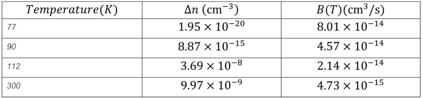
The radiative recombination coefficient is temperature dependent and it decreases with increasing temperature. Its temperature dependence is shown in table:
Table 5-1: Temperature dependence oft he radiative recombination coefficient
*^_E^`abd`^(f) ∆@ (cmgh) X(*)(cmh/s)
77 1.95 × 10g6? 8.01 × 10g>r
90 8.87 × 10g>u 4.57 × 10g>r
112 3.69 × 10gz 2.14 × 10g>r
5.2
Auger recombination
Auger recombination occurs when the energy released by the recombination of an electron-hole pair is carried off by a third free carrier. In lowly-injected p-type silicon, the third carrier is most likely to be a hole, and the corresponding recombination rate:
VL|JZW = }8∆@FP6 (5.5)
where } = 9.9 × 10ms is the low-injection Auger coefficient for p-type silicon. A similar expression holds for n-type silicon where !" = 2.8 × 10 cms .
The low-injection Auger lifetime then for p-type silicon is:
#$%&'( =!1
)* (5.6)
For low injection and:
#$%&'( =! 1
*∆, (5.7)
For high injection; where !* = 1.66 × 10/cms is the ambipolar Auger coefficient. Non interacting free particles should result in !* being equal to the sum of !" and !.
Like radiative recombination, Auger processes are intrinsic, in the sense that their presence does not depend on the specific techniques used for silicon crystal growth.
38 Recombination mechanisms
Figure 5-2: Example of Auger recombination
5.3
Recombination mediated by defects
Recombination center can act also as traps, in which a carrier is captured and subsequently injected back into the band from which it came. Trapping changes the free carrier concentration and can impact strongly on the overall carrier dynamics. We can write the first order differential equations in ∆, e∆3: 4'−7∆,7: =∆,# " = 1 #"/; (,/+ , + ∆,)(∆, − ∆3) ) +,∆,,/+ , @ (5.8) 4'−7∆37: =∆3# = 1 #/; (3/+ 3 + ∆3)(∆3 − ∆,) ) +3∆33/+ 3 @ (5.9)
Here 4' is the generation rate arising from external illumination and ,/ and 3/ are the electron and hole concentration in thermal equilibrium. #"/ and #/ are the fundamental electron and hole lifetimes and are related to the carrier thermal velocity ABC, the recombination center density N and the capture cross-sections D" andD of the center.
#/ = 1/)ABCD (5.10)
#"/ = 1/)ABCD" (5.11)
The factors , and 3 are the electron and hole densities when the Fermi level corresponds to the recombination center energy FG :
, = )H exp IFGJK L− FH (5.12)
3 = )Mexp IFH − FJKN − FGL (5.13)
where )H and )M are the effective densities of states at the conduction and valence band edges, and FH and FN are the conduction band energy and the band-gap energy.
The equations on the left of equation (5.8) and equation (5.9) define the carrier lifetimes in terms of the carrier densities and generation rate, which may be a function of time. The lifetime defined in this way is valid for arbitrary illumination conditions. If we consider the full equations, the aim is to solve them for #" and # in terms of ∆, or ∆3. Under steady-state conditions, when the derivative terms are zero, there exist general analytic solutions for #" and #.
In samples where the recombination center density N is relatively large, these full expressions should be used. If N is small compared to ∆, and ∆3 and the dopant density, the long expres-sions reduce to the expresexpres-sions of the Shockley-Read-Hall model. We can write this expression with the use of the following identities:
40 Recombination mechanisms ,/ ,/+ , = 3/ 3/+ 3 (5.14) And 3 , = 3/,/ (5.15) 4' =∆,# " = ∆3 # = ∆,3/+ ∆3,/+ ∆,∆3 #"/(3/+ 3 + ∆3) + #/(,/+ , + ∆,) (5.16)
In the SRH model, N is small: the trapping of the carriers by the centers is negligible in comparison to the excess densities and we can consider ∆, = ∆3. We can now write the equation for the recombination lifetime #OPQ = #" = # :
#OPQ = #"/(3/ + 3 + ∆,) + #, /(,/+ , + ∆,)
/+ 3/+ ∆, (5.17)
This equation reduces for p-type silicon to:
#OPQ =#"/()$+ 3 + ∆,) + #) /(, + ∆,)
This equation shows that the SRH lifetime is in general function of the excess carrier concentration. This equation could also be simplified in the case of very low and high injection.
In the case of deep centers, , and 3 are much smaller than )$ and ∆,, the expression be-comes:
#OPQ = #"/; 7SS3 S,:ST, VWX − Y,ZS:YW, (5.19)
#OPQ = #"/ + #/; 7SS3 S,:ST, ℎY4ℎ − Y,ZS:YW, (5.20)
Figure 5-3: SRH recombination lifetimes for two different resistivities and different values of #/
5.4
Surface recombination
Surface recombination is a special case of SRH recombination in which the localized states occur at the surface. These states, unlike bulk SRH centers, do not usually occupy a single energy level but form a set of states distributed across the band-gap. Analysis of the surface recombination is made in terms of surface recombination velocity.
42 Recombination mechanisms
In the simpler case, we can consider a sample with a constant bulk lifetime, #\, and a small con-stant SRV. The effective lifetime is:
1 #']] = 1 #\ + 2^ _ (5.21)
In the extreme case of infinite surface recombination velocity, the effective lifetime will be dominat-ed by the transit time of carriers to the surfaces, providdominat-ed the bulk lifetime is not very small. Under steady state conditions, the effective lifetime in this case is given by:
1 #']] = 1 #\ + 12` _ (5.22)
D is the carrier diffusivity. In low injection conditions should be used the value D for the minority
carriers while in high injection conditions an ambipolar diffusivity is more appropriate. This equation is used to estimate bulk lifetimes in samples with very high surface recombination velocities and low bulk lifetimes. In the transient decay mode, we have this equation:
1 #']] = 1 #\ + a` _ (5.23)
This amounts to a 22% higher effective lifetime measured in decay mode for a sample with a long bulk lifetime. For low bulk lifetime the difference is reduced.
5.5
Emitter recombination
Recombination within the heavily doped emitter region is another import source of carrier loss in silicon solar cells. Essentially, the high recombination rate in this region is due to Auger processes. It is possible to characterize total emitter recombination in terms of a single parameter: the emitter saturation current density, b/'. This parameter contains recombination at the emitter surface as well as within the emitter bulk.
The effective recombination lifetime due to the emitter can be written as:
#'dfBB'( = g, _
b/'()$ + ∆,) (5.24)
In conditions of low injection, the lifetime is injection-level independent but in high-injection condi-tions, it decreases linearly with excess carrier density. Values for b/' vary depending on the diffu-sion profile and the passivation quality.
5.6
Effective lifetime
For independent processes, the net recombination rate is the sum of all the single contributes, resulting in an effective lifetime #']]:
1 #']] = 1 #OPQ + 1 #$%&'( + 1 #'dfBB'( (5.25)
44 Surface passivation
Figure 5-4: Lifetime in function of excess carrier density for a substrate with )$ = 1 × 10 h cm and a deep SRH center with #"/ = 1 ms and #i = 1 s
In low injection, the sample is dominated by SRH recombination, at highest injection levels Auger recombination is the most important process.
6
Surface passivation
In order to minimize surface recombination, thin films of dielectric materials are used on crystalline solar cells as passivating layers. Surface passivation can be achieved mainly in two ways:
· reducing the recombination of charge carriers at the interface (chemical passivation)
· electrostatically, shielding the charge carriers from the interface by an internal electric field (field-effect passivation)
6.1
Chemical passivation
The chemical passivation mechanism reduces the surface recombination of charge carriers reducing the interface defect density.
We can write the equation for the surface recombination rate:[7]
jO = k,O3O − ,fl = n [, oBC`fB(FB)7FB O + , (FG)]D (FG) + [3O + 3 (FG)]D" (FG) tu tv (6.1) where:
jO= surface recombination rate per unit area
,O= electron density per unit volume at the cell surface
3O= hole density per unit volume at the cell surface
,f= intrinsic charge carrier density
D"= capture cross section of electron
D= capture cross section of hole
oBC= thermal velocity of charge
FG= Defect energy carrier level
`fB= Interface defect concentration
46 Surface passivation
From equation (6.1) we can see that the surface recombination rate is directly proportional to the Dit: a lower Dit value results in fact in a lower SRV.
The recombination is mainly due to the presence of dangling bonds and impurities at the surface. One way to reduce the recombination and thus lower the recombination velocity is by chemically saturating these dangling bonds with the application of a passivation layer (dielectric layer as Al2O3). Elements such hydrogen and oxygen atoms that are present in the passivation layer bind with the dangling bonds in order to make these trapping centers electrically inactive: lifetime of charge carriers will increase. Chemical passivation has the advantages that it is simple and low cost to apply and can be performed at room temperature.
6.2
Field effect passivation
Passivation can also be achieved electrostatically, shielding the charge carriers from the interface by an internal electric field. Due to the inclusion of additional charges into the semiconducting material, the minority charge carriers can be repelled from the cell surface to avoid recombination. This is called field effect passivation.
The first experimental attempts to reduce surface recombination losses in solar cells by means of the field effect passivation method were performed in the late 70s by Schartz et al.
Field effect passivation can be achieved in two ways: • Passivation through diffused surface
Through the additional doping of donor and acceptor atoms in the semiconductor, an additional electric field such as n+/p+ or n-/p- layer is formed near the cell surface and that repeals the minority charge carriers
• Passivation through fixed charges in the dielectric layer
Some passivation materials contain fixed positive or negative charges in the dielectric layers. These charges influence the movement of charge carriers. When a dielectric material containing negative charges such as Al2O3 is applied to p-type silicon, the high negative charge density in the pas-sivation layer acts as a shield and causes the repulsion of minority charge carriers, reducing the rate of charge carrier recombination at the interface. This results in a lower surface recombination velocity, SRV.
At the same way, when a dielectric material containing inherent positive charges such a SiNx is applied to p-type silicon, the high positive charge density at the interface attracts minority charge carriers. This causes the formation of an inversion layer at the interface between p-type silicon and the dielectric layers. We have a depletion of majority charge carriers, in this case holes, at the active recombination sites. Recombination rate at the surface is reduced.
6.3
A short review of surface passivation materials
Three of the most important surface passivation materials used for photovoltaic technologies are silicon dioxide, SiO2, hydrogenated amorphous silicon nitride, a-SiNx:H, and hydrogenated amor-phous Si, a-Si:H.
· Silicon dioxide,SiO2
The high quality of interface between thermally grown SiO2 and Si is responsible for high solar cell efficiencies . [8]Silicon thermal oxide layers allow for a surface recombination velocity of below 10 cm/s on p-type surfaces .[9] The passivation mechanism of these films is based on chemical passivation and that leads to a low interface trap density at the Si/SiO2 interface (Dyz ≈
48 Surface passivation
10 /cm ∙ eV ). Typical values for the positive fixed charge density are in the range of
1 to 5 × 10 cm [9].This high level of chemical passivation can be achieved for both n- and
p-type surfaces. Forming gas annealing for example introduces hydrogen that passivates the electronically active defects such as Pb-type defect that is a Si-dangling bond [2].
· Hydrogenated amorphous silicon nitride, a-SiNx:H
The optical properties of this material can be varied in a wide range; SiNx is in fact the standard material for antireflection coatings in solar cells. Films containing nitrogen exhibit refractive indices around 2: for this reason they are applied at the front of a solar cell. In addiction SiNx releases hydrogen during firing und this plays an important role in the bulk passivation of multicrystalline Si [10]. The passivation mechanisms of a-SiNx:H films depends on the content of nitrogen. For exam-ple, when the nitrogen content is low, the high level of passivation is mainly due to chemical pas-sivation. When the concentration of N is high, on the other hand, the films induce a significant amount of field effect passivation [2, 10].
· Hydrogenated amorphous Si, a-Si:H
The deposition of hydrogenated amorphous silicon (a-Si:H) is another way to obtain excellent passivation. In contrast to hydrogenated amorphous silicon nitride (a-SiNx: H), the amorphous silicon (a-Si: H) does not contain inherent positive charges in the dielectric layer. This avoids shunting at the rear surface and the recombination in the interface [11]. Limitation of the application of a-Si:H surface passivation films are parasitic absorption effects and the lack of thermal stability during firing [2].