CHAPTER 2
Optical Quality-Assessment of High-Order One-Dimensional Silicon
Photonic Crystals With a Reflectivity Notch at ~
ʎ 1:55 µm
Abstract
In this paper, high-order silicon/air vertical 1-D photonic crystals (PhCs) featuring a deep reflectivity notch (Q of about 3000) within the third telecommunication transmission window are fabricated by electrochemical micromachining of silicon and optically characterized. Although, from scanning electron microscope (SEM) investigations, the microfabricated structures appear to be of high quality in terms of in-plane and out-of-plane uniformity as well as of low surface roughness, optical measurements highlight variability of the spectral position of reflectivity notches, which turns out to be affected by fine variations of structural features induced by fabrication. A nondestructive optical method is used to recover the distribution of typical fabrication features, which is not easily quantifiable with other techniques in these high aspect-ratio vertical structures, from the experimentally detected distribution of the optical features. Optical distribution is obtained by scanning the device with high spatial resolution and recording spectral reflectivity at normal incidence (in the wavelength range 1.0–1.7 µm) on different locations of the 1-D PhC surface (X–Y plane).
Distribution of silicon thickness variation on the X–Y plane is then inferred by best fitting the experimental spectral reflectivity data with theoretical spectra that are calculated by taking into account nonidealities of both PhC structure and measuring setup. On-sample fabricationinduced variation of the average silicon thickness, as a function of the X–Y position, is estimated to be limited to ±80 nm (percentage error of ±1%) within a range of ±100 µm from a reference location. As a consequence of such thickness variation, a maximum shift of the reflectivity spectrum of 40 nm occurs as a function of the X–Y position in the range of ±100 µm. Sample-to-sample average silicon thickness variation among nominally equivalent structures is also tested in similar X–Y positions and found to be lower than ±1.5% (absolute variation of "±120 nm), within a range of ±15 µm, with respect to the average value on the investigated samples.
© 2010 IEEE. Reprinted, with permission, from G. Barillaro, S. Merlo, S. Surdo, L. M. Strambini, F. Carpignano, Optical Quality-Assessment of High-Order One-Dimensional Silicon Photonic Crystals With a Reflectivity Notch at ~1:55 µmʎ , Vol 2, Number 6,
1. Introduction
During the past 10 years, photonic crystal (PhC) structures have represented an important part of the silicon photonics [1]–[3]. An extensive PhC literature has been published on both theory and experiments, and 1-D, 2-D, and 3-D PhCs have been engineered to obtain devices with unique properties, such as high quality-factor resonators, sharp-bend waveguides, negative-refraction lenses, etc.
The principal motivation of the emergence of PhCs is the possibility of controlling light propagation at the wavelength scale. Periodical modulation of the PhC lattice constant (of the order of the operation wavelength) and exploitation of high-contrast refractive index materials are required to open up an optical bandgap in the dispersion relationship of the structure in a specific range around the operation wavelength. Structures based on air-void formation into silicon substrates by established (i.e., Potassium Hydroxide- KOH, Deep Reactive Ion Etching- DRIE) or emerging (i.e., Electrochemical MicromachiningV ECM) micromachining technologies are, thus, intrinsically good candidates for PhC realization due to the high contrast between the refractive index of silicon (nSi = 3.48 at 1.55 µm) and air (nAir = 1). Throughout the last decade, silicon-based 1-D [4]–[7], 2-D [8]–[10], and 3-D [11]–[13] PhCs have been actually fabricated by using different technologies. However, as optical phenomena in PhCs are based on their perfect periodicity and shape, structural disorder significantly affects their optical properties [14]–[18]. Among the different technologies proposed for PhC fabrication, silicon ECM has shown great potential thanks to its high flexibility that allows fabrication of 1-D [6], [15], [19], 2-D [8], [20], and 3-D [12], [21] PhC structures with high aspect-ratio and high uniformity to be performed at low cost. ECM is based on the electrochemical etching of silicon in a HF-based electrolyte under back-side illumination of the silicon substrate [22] and combines the advantages of dry and wet standard silicon etchings. ECM represents, thus far, a unique case of straightforward, low-cost wet etching with the microfabrication features that are typical of complex, very expensive dry-etching processes [23], [24].
In past years, we have successfully employed ECM for the fabrication of 1-D PhCs exploiting highorder bandgaps in the near-infrared spectral region, with high extinction-ratio between adjacent highand low-reflectivity bands, which are characterized by a reflectivity spectrumthat is highly sensitive to small changes in the materials assembling the photonic structures [6], [15], [25], [26]. In our previous papers, we reported the design, fabrication, and characterization of vertical silicon/air high-order 1-D PhCs featuring a high-order bandgap around a wavelength ʎ in the third transmission window of telecommunications. According to the so-called hybrid quarter-wavelength stack, they consist of periodic arrays of silicon layers with thickness dSi and air gaps of width dAir satisfying the conditions
dSi = M /4nʎ Si and dAir = N /4, where M and N are odd integer, independentʎ parameters, nSi is the silicon refractive index at (whereas air refractive index isʎ
1), and n=(M+ N)/ 2 is the order of the bandgap that is centered at ʎ [6]. However, when dealing with biosensing and optofluidic applications, high-order PhC structures having a high Q reflectivity minimum (notch), instead of a reflectivity maximum (bandgap), at the operation wavelength ~1ʎ .55 µm would be more appealing as they would allow better exploitation of high-sensitivity of the optical properties of the photonic structure to small changes (thickness and/or refractive index) of the structure materials [27], [28].
In this paper, we demonstrate that, by choosing even integer values for M and N, 1-D PhCs can be designed and fabricated featuring a narrow notch within the third telecommunication window, corresponding to a reflectivity minimum between two consecutive high-order bandgaps, which can be envisioned as a resonance peak with high quality-factor (Q) at the selected wavelength . Despite the high qualityʎ of the microfabricated structures, in terms of in-plane and out-of-plane uniformity as well as surface roughness, which is demonstrated by scanning electron microscope (SEM) investigations, we have observed that spectral position and quality factor of reflectivity notches may be affected by tiny variations of the structural features induced by fabrication, although they are not easily quantifiable by SEM observation. The existence of such reflectivity notches is related to the presence of transmissivity peaks originating from the superposition of the transmission transfer function of a cascade (along the Z-direction) of well-matched and tuned filters. Slight detuning of the filter cascade due to fabrication errors along the Z-direction and/or in the X–Y plane can affect the notch wavelength position and lead to a reduction of the quality factor value.
In this paper, quality assessment of electrochemical micromachined 1-D PhCs featuring a reflectivity notch in the third telecommunication transmission window is performed by an optical non destructive method. Optical feature distribution of 1-D PhCs is investigated by measuring spectral reflectivity variation on the X–Y plane around a reference location, through 1-D PhC surface high-resolution scanning ensured by a fiber-optic setup incorporating single-mode fibers, with a tapered lensed termination. Distribution of fabrication features on the X–Y plane, in particular silicon thickness and roughness variation, is inferred by best-fitting the experimental spectral reflectivity in the wavelength range 1.0–1.7 µm with the expected theoretical behaviour, which is obtained by numerical calculations based on the characteristic matrix method that is modified to take into account nonidealities of device structure and measuring setup. On-sample feature distribution is evaluated by applying the proposed method on different locations of the same sample. Finally, sample-to-sample feature variations are also investigated by application of the proposed method on equivalent locations of different samples that are fabricated by using the same nominal process parameters.
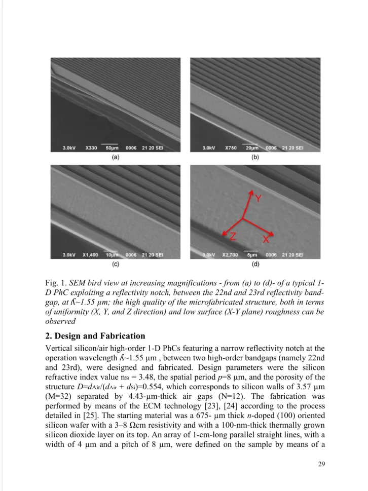
Fig. 1. SEM bird view at increasing magnifications - from (a) to (d)- of a typical
1-D PhC exploiting a reflectivity notch, between the 22nd and 23rd reflectivity band-gap, at ~1ʎ .55 µm; the high quality of the microfabricated structure, both in terms of uniformity (X, Y, and Z direction) and low surface (X-Y plane) roughness can be observed
2. Design and Fabrication
Vertical silicon/air high-order 1-D PhCs featuring a narrow reflectivity notch at the operation wavelength ~1ʎ .55 µm , between two high-order bandgaps (namely 22nd and 23rd), were designed and fabricated. Design parameters were the silicon refractive index value nSi = 3.48, the spatial period p=8 µm, and the porosity of the
structure D=dAir/(dAir + dSi)=0.554, which corresponds to silicon walls of 3.57 µm
(M=32) separated by 4.43-µm-thick air gaps (N=12). The fabrication was performed by means of the ECM technology [23], [24] according to the process detailed in [25]. The starting material was a 675- µm thick n-doped (100) oriented silicon wafer with a 3–8 Ωcm resistivity and with a 100-nm-thick thermally grown silicon dioxide layer on its top. An array of 1-cm-long parallel straight lines, with a width of 4 µm and a pitch of 8 µm, were defined on the sample by means of a
standard lithographic step. A buffered hydrofluoric acid (BHF) etch and a KOH etch were used to transfer the pattern in the silicon dioxide layer and in the silicon substrate, respectively. The KOH etch formed full V-grooves as initial seeds for the following electrochemical etching step.
Electrochemical etching in an HF- based solution (HF : H2O = 5%:95% by volume, with the addition of 1000 ppm of Sodium Lauryl Sulfate (SLS) used as surfactant) was then used to fabricate deep regular trenches in the patterned substrate. The etching voltage Vetch was set to a constant value of 3 V for the entire etching
process, while the etching current Ietch was set to an initial value Ietch0 = 23. 41 mA
over a circular etching area of 0.66 cm2 and properly reduced during the etching in
order to obtain a constant (nominal) porosity value of 55.4% through the entire etching depth [25]. The etching time tetch = 2400 s was chosen to fully etch
55-µm-deep trenches. After the electrochemical etching, a drying step aimed to the removal of the surfactant from the silicon surface and to the evaporation of the liquid filling the trenches was performed. Samples were cut along the X-direction to perform optical measurements of the reflectivity spectrum on the X–Y plane and, in some cases, along the Z-direction to accomplish SEM investigation of their cross-section.
A SEM bird-view at different magnifications of a typical 1-D PhC fabricated according to the technological process here described is reported in Fig. 1. The high quality of the microfabricated structure, in terms of uniformity (X, Y, and Z direction) and low surface (X–Y plane) roughness, is clearly reported.
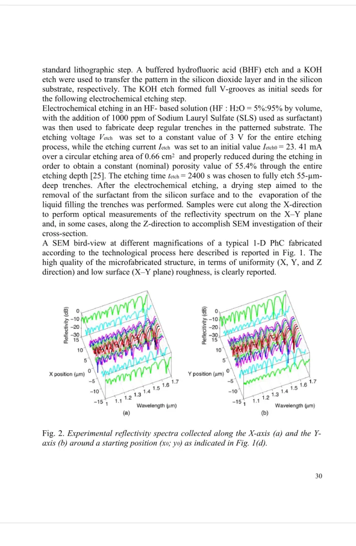
Fig. 2. Experimental reflectivity spectra collected along the X-axis (a) and the
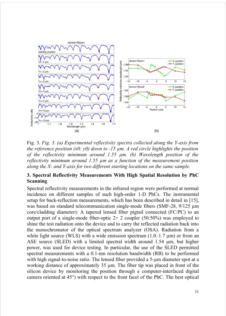
Fig. 3. Fig. 3. (a) Experimental reflectivity spectra collected along the Y-axis from
the reference position (x0; y0) down to -15 µm. A red circle highlights the position of the reflectivity minimum around 1.55 µm. (b) Wavelength position of the reflectivity minimum around 1.55 µm as a function of the measurement position along the X- and Y-axis for two different starting locations on the same sample. 3. Spectral Reflectivity Measurements With High Spatial Resolution by PhC Scanning
Spectral reflectivity measurements in the infrared region were performed at normal incidence on different samples of such high-order 1-D PhCs. The instrumental setup for back-reflection measurements, which has been described in detail in [15], was based on standard telecommunication single-mode fibers (SMF-28, 9/125 µm core/cladding diameter): A tapered lensed fiber pigtail connected (FC/PC) to an output port of a single-mode fiber-optic 2× 2 coupler (50:50%) was employed to shine the test radiation onto the device and to carry the reflected radiation back into the monochromator of the optical spectrum analyzer (OSA). Radiation from a white light source (WLS) with a wide emission spectrum (1.0–1.7 µm) or from an ASE source (SLED) with a limited spectral width around 1.54 µm, but higher power, was used for device testing. In particular, the use of the SLED permitted spectral measurements with a 0.1-nm resolution bandwidth (RB) to be performed with high signal-to-noise ratio. The lensed fiber provided a 5-µm diameter spot at a working distance of approximately 35 µm. The fiber tip was placed in front of the silicon device by monitoring the position through a computer-interfaced digital camera oriented at 45°) with respect to the front facet of the PhC. The best optical
fiber working distance was found by maximizing the back-reflected optical power in the wavelength regions corresponding to PhC bandgaps, using a manual translation stage to displace the fiber along the Z-axis. A two-axis, computer-controlled motorized translating holder was used to move the silicon device in the X–Y vertical plane. A high-resolution micro-translation stage (PI M-110.1 DG) performed vertical displacements of the silicon device along the Y-axis, whereas a precision linear translation stage (PI M-405 DG) was employed for displacements along the X-axis.
Optical feature distribution of 1-D PhCs was investigated around different locations (x0; y0) on the X–Y plane, with y0 always located in the middle with
respect to the silicon wall height (about 25 µm from top), as shown in Fig. 1(d). Reflected power spectra were acquired, starting from the reference position (x0;
y0), at increasing distances by performing controlled scans in the X–Y plane with
micrometer-size resolution steps (1 µm–50 µm). As starting points for the scans, position 1 was selected approximately at the center of the sample, and position 2 was taken on the side of the sample. In selecting a precise starting point for the scan, we just verified the absence of major visible defects such as, for example, a silicon wall breakage. On-sample feature distribution, as well as sample-to-sample optical feature variation, was investigated on devices that were fabricated by using the same nominal process parameters. Data processing was performed after all the measurements were terminated.
Power spectra were initially elaborated with the procedure described in [15], which allowed for a good estimation of the absolute spectral reflectivity of the device (though still including coupling losses between fiber and PhC) through normalization of the measured spectrum with respect to the calculated spectrum of an ideal reflector. Fig. 2(a) and (b) report a typical sequence of reflectivity spectra attained by scanning the X-axis and the Y-axis, respectively. The scanning steps were 1 µm in the range of ±5 µm around the reference position, whereas 5- µm steps were used outside this range.
Fig. 3(a) shows the normalized reflectivity spectra, after neglecting optical losses, collected by means of Y-scans from the reference position (x0; y0) down to -15
µm. As designed, the reflectivity notch around 1.55 µm between two high-order bandgaps characterizes all the collected reflectivity spectra. Good reproducibility of the line shape of the reflectivity spectrum at the different Y positions is evident, although a small red or blue shift of the whole spectrum as function of the Y position is also visible. A quantitative estimation of the optical feature distribution could be obtained by extracting the position of the reflectivity notch [highlighted with red circles in Fig. 3(a)] around the designed operation wavelength ~1ʎ .55 µm. Fig. 3(b) shows the variation, in terms of wavelength position, of the reflectivity notch along the X- and Y-axis for two reference locations on the same sample. A
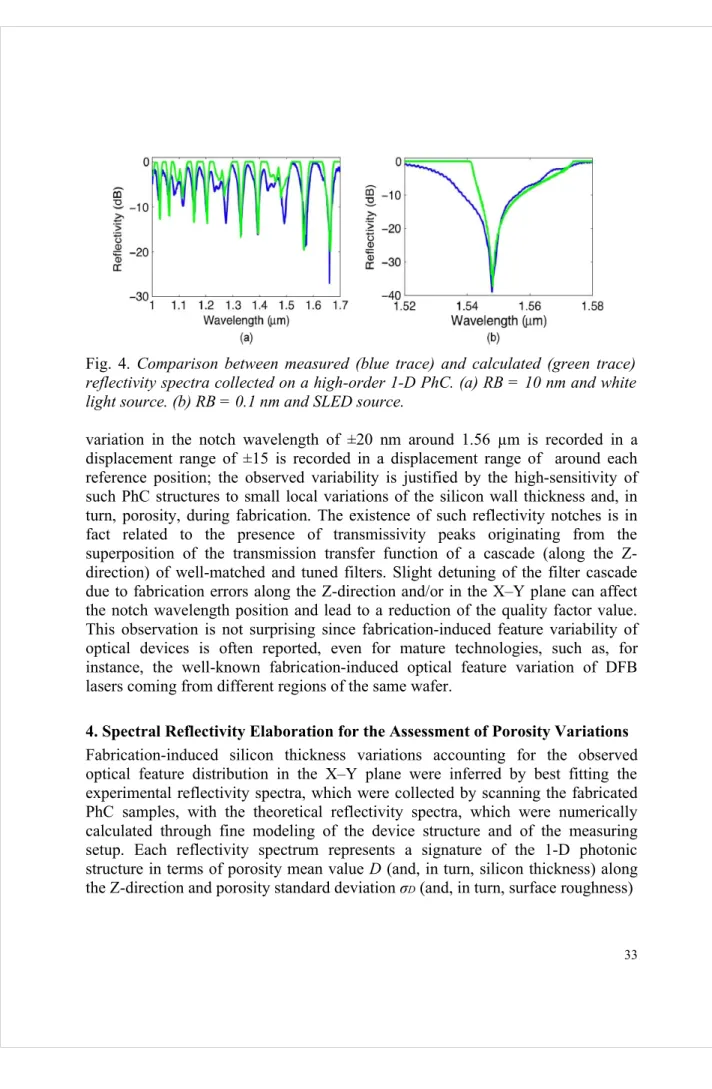
Fig. 4. Comparison between measured (blue trace) and calculated (green trace)
reflectivity spectra collected on a high-order 1-D PhC. (a) RB = 10 nm and white light source. (b) RB = 0.1 nm and SLED source.
variation in the notch wavelength of ±20 nm around 1.56 µm is recorded in a displacement range of ±15 is recorded in a displacement range of around each reference position; the observed variability is justified by the high-sensitivity of such PhC structures to small local variations of the silicon wall thickness and, in turn, porosity, during fabrication. The existence of such reflectivity notches is in fact related to the presence of transmissivity peaks originating from the superposition of the transmission transfer function of a cascade (along the Z-direction) of well-matched and tuned filters. Slight detuning of the filter cascade due to fabrication errors along the Z-direction and/or in the X–Y plane can affect the notch wavelength position and lead to a reduction of the quality factor value. This observation is not surprising since fabrication-induced feature variability of optical devices is often reported, even for mature technologies, such as, for instance, the well-known fabrication-induced optical feature variation of DFB lasers coming from different regions of the same wafer.
4. Spectral Reflectivity Elaboration for the Assessment of Porosity Variations
Fabrication-induced silicon thickness variations accounting for the observed optical feature distribution in the X–Y plane were inferred by best fitting the experimental reflectivity spectra, which were collected by scanning the fabricated PhC samples, with the theoretical reflectivity spectra, which were numerically calculated through fine modeling of the device structure and of the measuring setup. Each reflectivity spectrum represents a signature of the 1-D photonic structure in terms of porosity mean value D (and, in turn, silicon thickness) along the Z-direction and porosity standard deviation σD (and, in turn, surface roughness)
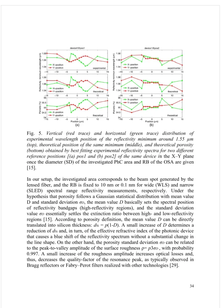
Fig. 5. Vertical (red trace) and horizontal (green trace) distribution of
experimental wavelength position of the reflectivity minimum around 1.55 µm (top), theoretical position of the same minimum (middle), and theoretical porosity (bottom) obtained by best fitting experimental reflectivity spectra for two different reference positions [(a) pos1 and (b) pos2] of the same device in the X–Y plane
once the diameter (SD) of the investigated PhC area and RB of the OSA are given [15].
In our setup, the investigated area corresponds to the beam spot generated by the lensed fiber, and the RB is fixed to 10 nm or 0.1 nm for wide (WLS) and narrow (SLED) spectral range reflectivity measurements, respectively. Under the hypothesis that porosity follows a Gaussian statistical distribution with mean value D and standard deviation σD, the mean value D basically sets the spectral position
of reflectivity bandgaps (high-reflectivity regions), and the standard deviation value σD essentially settles the extinction ratio between high- and low-reflectivity
regions [15]. According to porosity definition, the mean value D can be directly translated into silicon thickness: dSi = p(1-D). A small increase of D determines a
reduction of dSi and, in turn, of the effective refractive index of the photonic device
that causes a blue shift of the reflectivity spectrum without a substantial change in the line shape. On the other hand, the porosity standard deviation σD can be related
to the peak-to-valley amplitude of the surface roughness ρ= p3σD , with probability
0.997. A small increase of the roughness amplitude increases optical losses and, thus, decreases the quality-factor of the resonance peak, as typically observed in Bragg reflectors or Fabry–Perot filters realized with other technologies [29].
For every position interrogated during the scans, numerical simulations were performed to obtain the specific porosity mean value and standard deviation, yielding the best fit between theoretical and experimental reflectivity spectra, in order to quantify fabrication-induced silicon thickness variation on different locations of the X–Y plane accounting for optical feature distribution. As an example of the results of the fitting procedure, Fig. 4(a) shows an experimentally detected reflectivity spectrum (after normalization and neglecting optical losses) compared with the theoretically expected spectrum, calculated through best-fitting of the experimental data, using porosity mean value D and standard deviation σD as
fitting parameters, also taking into account the limited RB (RB = 10 nm) employed for the measurement and the beam spot-size (SD = 5 µm). The fitting procedure yielded D = 0:55 and σD = 1·10-4 for the experimental reflectivity spectrum of Fig.
4(a). Despite the complex line shape of the reflectivity spectrum of such high-order PhC structures, the agreement between measured and calculated spectra is rather good. In the reflectivity spectrum of Fig. 4(a), the extinction ratio between high- and low-reflectivity regions and the quality factor of the reflectivity notches are mainly limited by the low spectral resolution used in the measurement, as discussed in detail in [15]. In order to obtain a better estimation of the effective quality factor of the reflectivity notch, a SLED source was used to acquire the reflectivity spectrum on a narrow band around the chosen minimum with a RB = 0.1 nm, still ensuring a sufficiently high signal-to-noise ratio. Fig. 4(b) shows the experimental reflectivity spectrum collected using a SLED source, i.e., RB = 0.1 nm and SD = 5 µm, around the minimum at 1.548 µm and the theoretical reflectivity spectrum that is best fitted to the experimental one with D = 0.555 and
σD = 1·10-4. The quality factor of the reflectivity minimum was estimated to be
about 3000, which is rather high for 1-D PhCs that do not yet exploit specific resonant cavity structures.
5. On-Sample and Sample-to-Sample Optical Feature Distribution
Porosity mean values (and the corresponding theoretical wavelength positions of the reflectivity notch around 1.55 µm) obtained by best fitting all the reflectivity spectra of Fig. 2 are summarized in Fig. 5(a) as a function of the scanning position and are directly compared with the experimental wavelength positions of the same reflectivity notch. Fig. 5(b) reports similar results relative to an optical scanning performed around position 2 on the same sample. The porosity standard deviation values, which have been estimated with the fitting procedure, were in the range 1·10-4–1·10-3 and corresponded to roughness values ρ between 2.4–24 nm. The calculated spatial porosity distribution quantitatively matches and explains optical feature distribution, as indicated by the good agreement between the experimental shift of the notch wavelength and the theoretical shift resulting from the fitting procedure. As anticipated, and clearly visible in Fig. 5(a) and (b), higher porosity
values, corresponding to wider air gaps, lead to a lower effective refractive index of the photonic structure and, in turn, to a blue shift of the reflectivity spectrum and of the central wavelength of the minima; on the other hand, lower porosity values, corresponding to thicker silicon walls, lead to an effective refractive index increase and, in turn, to a red shift. The proposed approach offers a powerful, nondestructive method for quantifying fabrication-induced nonideality distribution of such PhCs, starting from and in addition to optical feature distribution. In fact, since the elevated optical quality of the surfaces of such high-order 1-D PhCs guarantees a sufficiently high quality factor to reliably detect the wavelength position of a reflectivity minimum, its distribution can actually be used to infer fine details in the optical feature distribution of the fabricated structures. On the other hand, by best fitting the experimental whole reflectivity spectrum with the theoretical reflectivity spectrum through fine modeling of both the photonic device and the measuring setup, the porosity distribution, i.e., silicon thickness (in terms of mean value and standard deviation) accounting for optical feature distribution can be obtained with higher resolution and reliability. Moreover, the proposed method could be further exploited to estimate other parameters such as, for example, the responsivity of PhC structures when used as a refractive index optical transducer.
Fig. 5 shows that variations of the optical features of electrochemically fabricated 1-D PhCs are strongly related, as expected, to local porosity variations, although these are limited to ±1% in a range of ±15 µm from the reference position. It is worth noting that a porosity mean value of 55% ±1%, as reported for the sample of Fig. 5, corresponds to average silicon wall thickness of 3.6 µm ± 0.08 µm, that is, a maximum average thickness variability on the X–Y plane of 80 nm on each side of the silicon walls. Local porosity variation of a few percentage points can be explained by supposing fluctuations, at the microscale, of the etching current density distribution in the X–Z plane of the sample during the etching process, which leads to the removal of slightly different silicon mass per unit time. For instance, for devices with porosity of 55% (etching current of 23.41 mA), a 1% absolute variation means a fluctuation in the etching current of about 400 µA throughout the etching areas. Although etching current fluctuation (in space and time) is actually an intrinsic characteristic of anodic dissolution of silicon in HF-based solutions (current burst- CB - model [30]) and is easily accountable for surface roughness of etched structures, porosity variation of a few percentage points cannot be easily explained in terms of the CB model. It is more likely that small lithographic errors (of the order of tens nanometers) due to the limited resolution (1 µm) of the lithography tool used in this work are slightly enhanced during the KOH etching step (for seed point formation) and are responsible for significant local variations of the etching current and, in turn, for porosity
lithographic tools with limited resolution, ECM of silicon is able to control silicon dissolution at the nanometric scale.
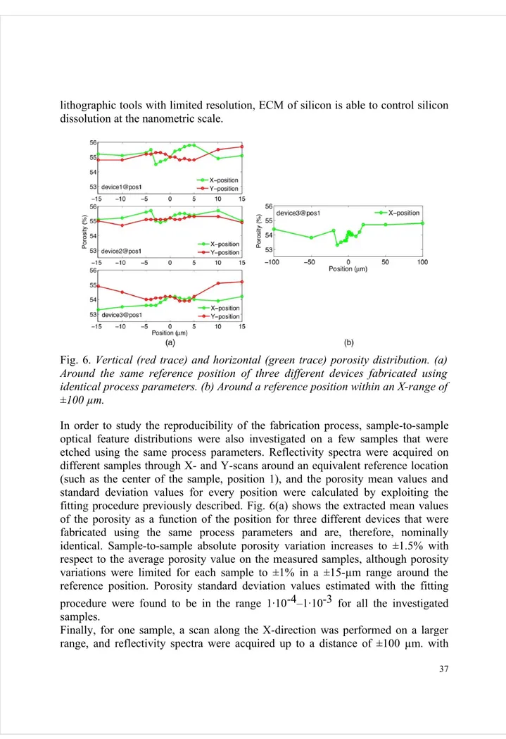
Fig. 6. Vertical (red trace) and horizontal (green trace) porosity distribution. (a)
Around the same reference position of three different devices fabricated using identical process parameters. (b) Around a reference position within an X-range of ±100 µm.
In order to study the reproducibility of the fabrication process, sample-to-sample optical feature distributions were also investigated on a few samples that were etched using the same process parameters. Reflectivity spectra were acquired on different samples through X- and Y-scans around an equivalent reference location (such as the center of the sample, position 1), and the porosity mean values and standard deviation values for every position were calculated by exploiting the fitting procedure previously described. Fig. 6(a) shows the extracted mean values of the porosity as a function of the position for three different devices that were fabricated using the same process parameters and are, therefore, nominally identical. Sample-to-sample absolute porosity variation increases to ±1.5% with respect to the average porosity value on the measured samples, although porosity variations were limited for each sample to ±1% in a ±15-µm range around the reference position. Porosity standard deviation values estimated with the fitting procedure were found to be in the range 1·10-4–1·10-3 for all the investigated samples.
Finally, for one sample, a scan along the X-direction was performed on a larger range, and reflectivity spectra were acquired up to a distance of ±100 µm. with
respect to the reference position. Porosity mean values, which were obtained by best fitting the measured reflectivity spectra, are reported as a function of the X-position in Fig. 6(b). A maximum absolute porosity variation of ±1% with respect to the reference location was found over the full-investigated range, thus providing a further assessment of the optical and fabrication feature distribution of 1-D PhCs produced by ECM. Porosity standard deviation values over the whole ±100 µm. interval were still found to be in the range 1·10-4–1·10-3
6. Conclusion
In this paper, fabrication and quality assessment of ECM-fabricated 1-D PhCs featuring a high quality-factor reflectivity notch in the near infrared region at ~ʎ 1:55 µm was performed. A 40-nm maximum experimental shift of the near infrared reflectivity depending on the measurement position on the X–Y plane (over a range of ±100 µm around a reference location) was found as a consequence of 80-nm-maximum fabrication-induced silicon thickness variation with respect to the average value. A peak-to-valley surface roughness in the range 2.4–24 nm depending on the X–Y plane position was also found superposed to thickness variation. On one hand, small lithographic errors (of the order of tens nanometers) due to the limited resolution (1 µm) of the lithography tool used in this work is hypothesized to be mostly responsible for local variations of the etching current in the range of hundreds of microamperes accounting for average thickness variations. On the other hand, ECM intrinsic etching current fluctuation is likely to be associated with surface roughness. A nondestructive optical method was successfully employed based on numerical fitting of experimental reflectivity spectra, which were acquired at normal incidence in the wavelength range 1.0–1.7 µm by scanning the X and Y-axis with micrometer-size steps, through fine modeling of the device structure and of the measuring setup. The proposed method allows estimation of silicon thickness variations (mean value and standard deviation) with good accuracy and reliability from reflectivity measurements performed over a large spectral range and will be exploited in the near future to estimate other parameters such as, for example, the responsivity of PhC structures when used as a refractive index sensor.
References
_________________________________________________________________ [1] R. Soref, “Silicon photonics: A review of recent literature”, Silicon, vol. 2, no. 1, pp. 1– 6, Jan. 2010.
[2] R. Soref, “The past, present, and future of silicon photonics”, IEEE J. Sel. Topics
Quantum Electron., vol. 12, no. 6, pp. 1678–1687, Nov./Dec. 2006.
[3] R. Soref, “The achievements and challenges of silicon photonics”, Adv. Opt. Technol., vol. 2008, pp. 1–7, 2008.
[4] A. Tolmachev, L. S. Granitsyna, E. N. Vlasova, B. Z. Volchek, A. V. Nashchekin, A. D. Remenyuk, and E. V. Astrova, “One-dimensional photonic crystal obtained by vertical anisotropic etching of silicon”, Semiconductors, vol. 36, no. 8, pp. 932–935, Aug. 2002. [5] B. Saadany, M. Malak, M. Kubota, F. Marty, Y. Mita, D. Khalil, and T. Bourouina, “Free-space tunable and drop optical filters using vertical Bragg mirrors on silicon”, IEEE
J. Sel. Topics Quantum Electron., vol. 12, no. 6, pp. 1480–1488, Nov./Dec. 2006.
[6] G. Barillaro, A. Diligenti, M. Benedetti, and S. Merlo, “Silicon micromachined periodic structures for optical applications at λ = 1:55 µm”, Appl. Phys. Lett., vol. 89, no. 15, pp. 151110-1–151110-3, Oct. 2006.
[7] A. Lipson and E. M. Yeatman, “A 1-D photonic band gap tunable optical filter in (110) silicon”, J. Microelectromech. Syst., vol. 16, no. 3, pp. 521–527, Jun. 2007.
[8] U. Grü ning and V. Lehmann, “Two-dimensional infrared photonic crystal based on macroporous silicon”, Thin Solid Films, vol. 276, no. 1/2, pp. 151–154, Apr. 1996.
[9] A. Chelnokov, S. David, K. Wang, F. Marty, and J.-M. Lourtioz, “Fabrication of 2-D and 3-D silicon photonic crystals by deep etching”, IEEE J. Sel. Topics Quantum Electron., vol. 8, no. 4, pp. 919–927, Jul./Aug. 2002.
[10] Y. Akahane, T. Asano, B.-S. Song, and S. Noda, “High-Q photonic nanocavity in a two-dimensional photonic crystal”, Nature, vol. 425, no. 6961, pp. 944–947, Oct. 2003. [11] S. Y. Lin, J. G. Fleming, D. L. Hetherington, B. K. Smith, R. Biswas, K. M. Ho, M. M. Sigalas, W. Zubrzycki, S. R. Kurtz, and J. Bur, “A three-dimensional photonic crystal operating at infrared wavelengths”, Nature, vol. 394, no. 6690, pp. 251–253, Jul. 1998.
[12] S. Matthias, F. Mu¨ ller, C. Jamois, R. B. Wehrspohn, and U. Go¨ sele, “Large-area three-dimensional structuring by electrochemical etching and lithography”, Adv. Mater., vol. 16, no. 23/24, pp. 2166–2170, Dec. 2004.
[13] A. Ledermann, L. Cademartiri, M. Hermatschweiler, C. Toninelli, G. A. Ozin, D. S. Wiersma, M. Wegener, and G. Von Freymann, “Three-dimensional silicon inverse photonic quasicrystals for infrared wavelengths”, Nat. Mater., vol. 5, no. 12, pp. 942–945, Dec. 2006.
[14] X. Lu, P. Han, Y. Quan, Q. Ran, L. Gao, F. Zeng, C. Zhao, and J. Yu, “Optical response of high-order band gap in onedimensional photonic crystal applying in-plane integration”, Opt. Commun., vol. 277, no. 2, pp. 315–321, Sep. 2007.
[15] G. Barillaro, L. M. Strambini, V. Annovazzi-Lodi, and S. Merlo, “Optical characterization of high-order 1-D silicon photonic crystals”, IEEE J. Sel. Topics Quantum
Electron., vol. 15, no. 5, pp. 1359–1367, Sep./Oct. 2009.
[16] D. Gerace and L. C. Andreani, “Effects of disorder on propagation losses and cavity Q-factors in photonic crystal slabs”, Photon. Nanostruct.-Fundam. Appl., vol. 3, no. 2/3, pp. 120–128, Dec. 2005.
[17] A. Femius Koenderink, A. Lagewndijk, and W. L. Vos, “Optical extinction due to intrinsic structural variations of photonic crystals”, Phys. Rev. B, Condens. Matter, vol. 72, no. 15, p. 153 102, Oct. 2005.
[18] S. Matthias, R. Hillebrand, F. Müller, and U. Gösele, “Macroporous silicon: Homogeneity investigations and fabrication tolerances of a simple cubic three-dimensional photonic crystal”, J. Appl. Phys., vol. 99, no. 11, pp. 113102-1–113102-5, Jun. 2006. [19] E. V. Astrova, V. A. Tolmachev, G. V. Fedulova, V. A. Melnikov, A. V. Ankudinov, and T. S. Perova, “Optical properties of one-dimensional photonic crystals fabricated by photo-electrochemical etching of silicon”, Appl. Phys. A, vol. 98, no. 3, pp. 571–581, Mar. 2010.
[20] Z. Kral, J. Ferre` -Borrull, J. Pallares, T. Trifonov, A. Rodriguez, R. Alcubilla, and L. F. Marsala, “Characterization of 2D macroporous silicon photonic crystals: Improving the photonic band identification in angular-dependent reflection spectroscopy in the mid-IR”,
[21] M. Garín, T. Trifonov, A. Rodrı´guez, L. F. Marsal, and R. Alcubilla, “Optical properties of 3D macroporous silicon structures”, Mater. Sci. Eng. B, vol. 149, no. 3, pp. 275–280, Apr. 2008.
[22] V. Lehmann and H. Föll, “Formation mechanism and properties of electrochemically etched trenches in n-type silicon”, J. Electrochem. Soc., vol. 137, no. 2, pp. 653–659, 1990. [23] G. Barillaro, A. Nannini, and M. Piotto, “Electrochemical etching in HF solution for silicon micromachining”, Sens. Actuators A, Phys., vol. 102, no. 1/2, pp. 195–201, Dec. 2002.
[24] G. Barillaro, P. Bruschi, A. Diligenti, and A. Nannini, “Fabrication of regular silicon microstructures by photoelectrochemical etching of silicon”, Phys. Stat. Sol. (C), vol. 2, no. 9, pp. 3198–3202, Jun. 2005.
[25] G. Barillaro, L. M. Strambini, and S. Merlo, “Band gap tuning of silicon micromachined 1D photonic crystals by thermal oxidation”, IEEE J. Sel. Topics Quantum
Electron., vol. 14, no. 4, pp. 1074–1081, Jul./Aug. 2008.
[26] G. Barillaro, S. Merlo, and L. M. Strambini, “Optical characterization of alcohol-infiltrated one-dimensional silicon photonic crystals”, Opt. Lett., vol. 34, no. 12, pp. 1912– 1914, Jun. 2009.
[27] S. M. Weiss, G. Rong, and J. L. Lawrie, “Current status and outlook for silicon-based optical biosensors”, Phys. E, vol. 41, no. 6, pp. 1071–1075, May 2009.
[28] K. B. Mogensen and J. P. Kutter, “Optical detection in microfluidic systems”,
Electrophoresis, vol. 30, no. S1, pp. S92–S100, Jun. 2009.
[29] T. Asano, B.-S. Song, and S. Noda, “Analysis of the experimental Q factors (~1 million) of photonic crystal nanocavities”, Opt. Express, vol. 14, no. 5, pp. 1996–2002, Mar. 2006.
[30] H. Föll, M. Christophersen, J. Carstensen, and G. Hasse, “Formation and application of porous silicon”, Mater. Sci. Eng. R, vol. 39, no. 4, pp. 93–141, Nov. 2002.