Micro-structural modifications of
semiconductor systems under
irradiation: experiment, modeling
and simulation analysis.
Giuseppe Fisicaro
PhD in Physics XXIV Cycle
Department of Physics and Astronomy
Supervisor: Dr. Antonino La Magna PhD Coordinator: Prof. Francesco Riggi
Keywords: laser annealing, silicon, defects, dopant activation, dopant pile-up, simulation, modeling, Kinetic Monte Carlo.
An electronic version of this thesis, including color figures, is available at: http://dspace.unict.it/jspui/
a.a. 2008/2011
Copyright©2011 by Giuseppe Fisicaro
All rights reserved. No part of the material protected by this copyright notice may be reproduced or utilized in any form or by any means, electronic or mechanical, including photocopying, recording or by any information storage and retrieval system, without permission from the author.
Contents
Abstract 1
Introduction 3
1. Laser annealing of semiconductors: a general overview 11
1.1. Overview . . . 11
1.2. Laser processing of semiconductors: historical survey . 12 1.3. The thermal problem for non-melting laser processes . 16 1.3.1. Cristallization of amorphus silicon by scanning millisecond laser annealing . . . 19
1.3.2. Irradiation of multi-layer structures . . . 26
1.4. The melting problem . . . 28
1.4.1. Front tracking model . . . 29
1.4.2. Enthalpy model . . . 30
1.4.3. Phase field methodology . . . 31
1.5. The challenge to activate implanted dopant atoms by laser annealing . . . 36
1.5.1. Dopant evolution in the millisecond scale . . . 37
1.5.2. Melting and non-melting dopant evolution for pulsed nanosecond irradiation . . . 40
1.6. Modeling challenges . . . 43
2. Continuum modeling of submicrosecond defect kinetics in silicon under laser irradiation 45 2.1. Overview . . . 45
2.2. Introduction . . . 45
2.3. Defects in silicon . . . 47
2.4. Continuum model . . . 51
2.4.1. Thermal problem . . . 51
2.4.2. Defect system model . . . 52
2.5. Experiment . . . 56
2.6. Results and discussion . . . 61
2.6.1. The initialization problem . . . 61
2.6.2. Single implanted silicon structure . . . 65
2.6.3. Double implanted silicon structure . . . 68
2.7. Conclusion . . . 71
3. Continuum modeling of dopant-defects system evolution in silicon 73 3.1. Overview . . . 73
3.2. Introduction . . . 74
3.3. Dopant evolution in solid phase . . . 77
3.3.1. Dopant-defect interaction in silicon: the case of phosphorus . . . 77
3.3.2. Experimental approach . . . 81
3.3.3. Simulation modeling . . . 85
3.3.4. Results and discussion . . . 87
3.4. Dopant evolution in melting phase . . . 95
3.4.1. Experimental approach . . . 96
3.4.2. Continuum model . . . 97
3.4.3. Results and discussion . . . 99
3.5. Future prospects . . . 105
4. Kinetic Monte Carlo simulations of laser irradiation pro-cesses 107 4.1. Overview . . . 107
4.2. Introduction . . . 107
4.3. Kinetic Monte Carlo approach . . . 109
4.3.1. KMC code for the defect system in silicon . . . 113
4.3.2. Coupling between KMC and continuum field . 115 4.4. Comparison and links between PDE and KMC approaches116 4.4.1. Constant temperature process . . . 117
4.4.2. Laser annealing process . . . 120
Contents
5. Laser annealing of SiGe and Ge based devices 129 5.1. Overview . . . 129 5.2. Introduction . . . 130 5.3. LTA simulation approach for Si-Ge structures . . . 131 5.4. Simulation results in non-patterned and patterned
sam-ples . . . 133 5.5. Discussion . . . 137 A. Finite element method and Comsol code 139 B. Binar Collision Approximation (BCA) 143 C. Wheeler phase-field formulation 147
Acknowledgments 157
Curriculum Vitae 159
List of Publications 161
Abstract
Research on the micro-structural modifications of semiconductor sys-tems has played a central role in the last decades. In particular, Laser Thermal Annealing receives a great interest in the formation of ultra-shallow junctions essential in nanoscale metal-oxide-semiconductor technology. An intriguing poorly understood issue is the post-implant kinetics of the defects-dopant system in the extremely far-from-the equilibrium conditions caused by the laser irradiation both in the non-melting and melting regime. For this purpose, the activation mechanism in the solid phase of phosphorus implanted silicon under excimer laser irradiation has been investigated by means of experi-mental analysis and modeling. The models have been originally for-mulated and implemented in numerical codes, which belong to the class of the continuum (based on Partial Differential Equations) and atomistic (Kinetic Monte Carlo) approaches for kinetic simulation of the dopant-defect system under laser irradiation. Continuum mod-els will be also presented which clarified the boron non-equilibrium segregation during the fast solidification, i.e. the dopant pile-up phe-nomenon at the maximum melt depth. We will elucidate the dopant evolution mechanism in the melting phase considering the possibility of two different states governing the dopant diffusion in a tight tem-perature range around the melting temtem-perature. Finally, an accurate study of the feasibility of laser irradiation as a heat source for real patterned substrates has been carried out for the case of SiGe and Ge based MOS devices. We developed a continuum simulation code which simulates the interaction between the laser light and the tran-sistor periodic structure in order to estimate the heat source as well as the heat diffusion, phase changes and material redistribution under irradiation.
Introduction
Research on the micro-structural modifications of semiconductor sys-tems started at the beginning of the 50’s and the 60’s. Researchers were looking to replace the electrical components of that time, namely electron tubes, turning them to semiconductor devices. This class of materials were highly valued because they could be used as diodes due to their gap on the conduction band, allowing electron- or hole-type conduction if doped with different impurities. The first semiconductor-based device was produced by Russell Ohl of the Bell Telephone Lab-oratories and his group. This prototype acted like an electron tube diode exploiting the conductance properties of a junction formed by two oppositely doped samples of germanium. Subsequently, John Bardeen and Walter Brattain developed a device that worked not only as a diode valve but also as an amplifier. This ”point-contact transistor” was made-up by a slice of germanium with a few carefully placed wires touching it. Development and engineering of germanium transistors was unfeasible due to a series of technological problems and researchers focused their attention on other semiconductor materials. They found the answers to the majority of these problems in silicon and its oxide SiO2.
Silicon gained a central role in the microelectronics area thanks to its appropriate gap on the conduction band (a middle way between pure insulators and conductors), which allowed the fabrication of electronic devices on the micrometer and, nowadays, nanometer scale. On the other hand, advantages came also from the well controlled manipula-tion of its conducmanipula-tion properties by the addimanipula-tion of impurities. Differently from a metal, in a semiconductor the current conduction can occur via mobile or ”free” electrons and holes, collectively known as charge carriers. An intrinsic semiconductor, not being quite an
insulator, contains a small concentration of free electrons at room temperature. Since this concentration has been created by freeing electrons from bonds, an equal number of holes must also be present. The possibility of both carriers co-existing is vital to the operation of devices.
Doping a semiconductor such as silicon with a small amount of impu-rity atoms, such as phosphorus or boron, greatly increases the number of free electrons or holes within the semiconductor. The semiconduc-tor material used in devices is doped under highly controlled con-ditions in a fabrication facility to precisely control the location and concentration of p- and n-type dopants.
Generally dopant atoms are introduced in a semiconductor substrate by means of ion implantation, being this technique the most feasible and scalable for large-scale device fabrication. The interaction be-tween penetrating ions and the material atoms cause undesired defect cascades, just inside the implanted region. Subsequently, in order to restore the crystalline order and displace impurity atoms in substitu-tional positions (where they become electrically active), heat treat-ments become necessary. This process significantly affects the initial impurity density profile due to the thermal activated diffusion which can be modeled by means of the Fick-law. The solutions of the related diffusion equation has contributed to the predictions of the thermal process results and, as a consequence, to the accurate process control in the early generations of microelectronic devices.
However, the further developments posed new fundamental questions which did not find the correct understanding in the framework of the thermal equilibrium diffusion. Indeed, for thermal process in the time scale of few tens of seconds and below, non-equilibrium kinetics of the coupled system point defects-impurities dominate the impurity redis-tribution. From this point of view, an increasing interest raised on the investigation of the non-equilibrium caused by a point defect excess and in the role played by this excess in the dopant transient enhanced diffusion (TED) phenomena in Si. As a consequence, being the defect super-saturation the only relevant driving force of the non-equilibrium kinetics, the different stages (diffusion, aggregate nucleation, forma-tion and annihilaforma-tion of extended defects) of the defect evoluforma-tion in
Introduction
Si at quasi-constant temperature are now well known. Moreover, a consistent modeling approach has been derived and validated by ex-perimental works [30, 71, 91].
In order to fabricate smaller and smaller microelectronic devices, the current trend of the dopant activation process in Si is characterized by an extreme reduction of the annealing time (from the ms to ns regime for the ultra-fast thermal processes) and a correspondent increase of the peak temperature, eventually using the laser irradiation (LI) as a heat source [49, 50, 70, 105]. These processes should complement or substitute the actual rapid thermal annealing in the activation module of future nanoelectronic devices.
The extreme consequences of these concepts find their realization in the laser melting processes. The advantages offered by the Laser Ther-mal Annealing (LTA) process in the melting regime, compared to con-ventional Rapid Thermal Anneal (RTA) procedures, are represented by a better control of the junction depth and a higher dopant activa-tion efficiency. Indeed, the LTA causes the melting of a well defined region in the Si sample (with the melting depth depending essen-tially on the laser beam energy), where the dopant atoms redistribute themselves uniformly due to their huge diffusivity (∼ 10−4cm2/s in
the liquid phase), orders of magnitude higher than in the solid phase. Moreover, the non-equilibrium segregation during the fast solidifica-tion phenomenon, occurring after irradiasolidifica-tion, enhances dopant trap-ping and favors the incorporation of a high density of dopant atoms in substitutional positions.
Although the junction depth can be easily defined using LTA, the con-trol of the LTA process is far from being satisfactory. In particular, the LTA process integration in the process sequence applied to device manufacturing is critical. The most important problems concern the precise dopant profile definition in the two dimensional (2D) device geometry, the optimization of the LTA conditions (substrate temper-ature, pulse energy, number of pulses) on the basis of the required profile depth and shape, the effect of LTA on pre-formed structures (e.g. dielectric and polysilicon films), and the role of defects remaining after the LTA process.
As a consequence the predictions of the process results are funda-mental, and we have dedicated chapter 1 to the presentation of the state-of-the-art modeling approaches of the LTA simulation, consid-ering also particular applications to a series of experimental works which we have supported with simulations during the PhD period. Conventional modelling [105, 106] of the dopant distribution during LTA is based on the numerical solution of the heat diffusion equa-tion, that allows to simulate the liquid-solid interface evolution. Fur-thermore, the dopant diffusion is based on a sharp-interface model of the alloy solidification and a step-like change of the mass transport properties across the interface. The matching between the solutions in the liquid and solid zones at the solid-liquid interface is obtained from the mass conservation and from a segregation model ruling the jump in concentration across the interface itself. The sharp-interface model, which decouples thermal and mass evolution and does not con-sider the physical properties of the interface layer itself, allows only a phenomenological approach of the segregation problem. Indeed, the dependence of the segregation coefficient on the interface speed can be included by fitting the experimental results. However, an obvious computational drawback of this methodology is that the instantaneous interface position and speed should be tracked down. This introduces some limitations, in particular for the applications of 2D calculations or the cases where the whole device structure must be considered. The phase-field methodology [3, 15] improves the physical description of the moving phase boundary problem by considering a finite dimen-sion of the transition region between the two phases. The boundary lo-cation can be, in principle, tracked as a level set of the phase function. However, such tracking is not needed for the problem solution since phase, temperature and dopant density evolve concurrently according to three coupled differential equations. Therefore, the dopant redis-tribution is automatically evaluated solving the complete evolution problem. In this thesis work the phase-field method is our preferred approach to simulate thermal field and dopant density evolution dur-ing the LTA process. In spite to its rather complicated formulation, we can consider the phase-field as the ”zero order” model for the LTA simulation, i.e the analogous of the Fick diffusion law in the
simula-Introduction
tion of the conventional thermal process. It is the starting point of the model that we have originally formulated, implemented and applied during the PhD period.
Indeed, the post-implant kinetics of the defects–dopant system in the extremely far-from-the equilibrium conditions caused by the laser ir-radiation both in the non-melting and the melting regime is almost totally unknown and cannot be modeled with the standard phase field equations. From the theoretical point of view some relevant questions have to be addressed: the formalization of a reliable kinetic formalism for the evolving defect-impurity system in a non-uniform fast-varying thermal field [25, 26, 37, 53], the generalization of the kinetic parame-ters (e.g. diffusivity, clustering rate constants, etc.) in this regime, the inclusion in the formalism of eventual phase transitions [49], the inter-action between the defects generated by the implant and the defects generated by the process [52].
We will present our investigation and the achieved results concerning the evolution of the dopant-defect system in implanted silicon un-der LTA in the chapter 2 and chapter 3 of the present thesis. The case of phosphorus doping will be dealt in detail, focusing the at-tention on the activation mechanism under excimer laser irradiation. For this purpose, the activation efficiency in the solid phase has been measured in a wide range of irradiation conditions, varying the laser fluence and the number of shots. The total active fraction varies in a range spanning several orders of magnitude and shows a com-plex trend depending on the process conditions. We investigated this system developing a continuum models, formed by a set of coupled Partial Differential Equations (PDE model), which allow for an accu-rate determination of thermal fields and melting evolution by means of the phase-field methodology [41, 49, 50]. This last equations have been coupled with a diffusion-reaction model which can simulate the evolution of the dopant-defects system during the annealing process [25, 26, 37, 53]. Our continuum model will be able to explain the whole scenario[25, 26].
In the second part of chapter 3, we will discuss widely our investigation on the dopant evolution mechanism in the melting phase of boron implanted silicon under laser irradiation. In particular, laser processes
where the maximum melt depth is much larger than the implanted B ion projected range are considered (i.e. the implantation defects are fully annihilated by the melting). Experimental analysis suggests that the dopant evolution and its redistribution in the molten regions can be divided in three different regimes as a function of the laser fluence (or the maximum melt depth): against-gradient, pile-up and no-pile-up regimes. We will elucidate the dopant evolution mechanism in the melting phase considering the possibility of two different states governing the dopant diffusion in a tight temperature range around the melting temperature.
We will try to demonstrate that simulations of laser processes are crucial in order to understand the effects of irradiation on material modification both in the melting and solid phase. It is due to the in-trinsic features of the laser annealing processes (evolution of bulk and surface material properties on a scale less than micro and nanosec-onds). Within continuum models the entire physics of the system is formulated as a set of differential equations ruling the density field kinetics of each particle considered to be relevant in the process. This technique has the advantages to be easily implemented in commercial simulation tools with a quick setting of the problem. Moreover, in gen-eral, the simulation time is short and large systems can be studied by adjusting the grid used for the spatial discretization of the equations. Most of these limitations can be overcome tackling the problem with a Kinetic Monte Carlo (KMC) approach. In this way, there are no limitations in the number of interactions between dopant atoms and defects. A detailed dopant clustering can be considered as well as dopant-defect cluster complexes (in a explicit way than done until now). At the same time, great part of the parameters will be di-rectly extracted from atomistic calculations. We have developed an innovative KMC code, which rules the post-implant kinetics of the defects-dopant system in the extremely far-from-the equilibrium con-ditions caused by the laser irradiation both in the non-melting, melt-ing and partial meltmelt-ing regimes. In chapter 4 the KMC approach will be described in detail and its results will be compared with a similar simulation analysis carried out by means of the continuum model. The previous research issues have been conducted from a fundamental
Introduction
point of view in non-patterned structures. However, for application purposes, due to the comparable dimensions of the nano-device pe-riodic structure and the laser wave length, an accurate study of the feasibility of laser irradiation as a heat source for real patterned sub-strates is needed. This study reveals some crucial drawbacks when applied to conventional Si based devices. In this sense, laser irradia-tion brings the technology back to the beginning of microelectronics. Indeed, the application of this process seems more effective in the case of Ge and Ge-based devices.
Therefore a deeper analysis of the integration of laser annealing in SiGe and Ge-based MOS devices is needed. We developed a simula-tion code based on two modules: the former simulates the interacsimula-tion between the laser light and the transistor structure in order to es-timate the heat source. The latter simulates heat diffusion, phase changes and material redistribution under irradiation and it corre-sponds to the two-dimensional case of the approach described in the first chapter. The model is calibrated in the case of different atomic species (namely Si, Ge and common dopant impurities), considering the thermal properties of the materials and the impurity-dependent diffusivity in the solid, liquid and interface region. In chapter 5, we present several simulation results obtained by varying materials, im-planted impurity profiles and geometry of the Complementary Metal Oxide Semiconductor (CMOS)-like structures. With the support of the simulation results we discuss the possible perspectives of excimer laser annealing applications for the fabrication of post-Si CMOS de-vices [27].
1. Laser annealing of
semiconductors: a general
overview
1.1. Overview
The introduction and the subsequent investigation of laser irradia-tion in order to modify material properties has a parallel origin to the laser development. At the beginning of the 50’s and the 60’s, several research groups started to investigate the feasibility to pro-duce coherent micro- and nanometer electromagnetic waves, both in pulsed and continuous emission. Early Maser (Microwave Amplifi-cation by Stimulated Emission of Radiation) equipments, exploiting Einstein theory on the stimulated light emission of excited systems, were based on the dis-excitation of a gas (ammonia) or solid state materials (chrome-ruby). Subsequently, the need to produce visible electromagnetic waves led to Laser (Light Amplification by Stimu-lated Emission of Radiation) devices. As maser systems, they were based on the dis-excitation of a gas system (helium-neon) or solid state materials (ruby, gallium arsenide).
The introduction of semiconductor-based laser allowed researchers to use stimulated light in continuous emission. In order to improve the device performances and their application, the effects of laser irra-diation on the irradiated materials started to stimulate the interest of several scientists. From this point to the present days, important results have been achieved. Due to the intrinsic features of the laser annealing processes (evolution of bulk and surface material proper-ties on a scale less than micro and nanosecond), an intensive use of
computer simulation supported the whole investigation journey. Con-cerning the chapter content, after a brief historical survey, we will deal with some interesting cases where material modifications are provoked by millisecond (continuous scanning) and nanosecond (pulsed) laser annealing. Starting from experimental observations, the investigation will be carried out mainly by means of simulations and the proper theoretical models will be presented.
1.2. Laser processing of semiconductors:
historical survey
The history of the investigation of the physical properties of semi-conductors starts at the beginning of the 60’s with several groups of research in the Soviet Union and the USA [7, 8, 9, 65].
In this first phase, the optical properties and recombination in strongly excited silicon was experimentally studied. Blinov investigated an unusual behavior of reflectivity increase from the surface of a strongly excited semiconductor and suggested that it was due to the melting of a thin surface layer, which exhibits metal properties.
Laser annealing of implanted layer was investigated for the first time by the Philipovich group in 1974 [74]. In the same year, using a heavy dose Phosphorus implant annealed by laser, another research grop directed by Prof. Khaibullin (University of Kazan) studied the effects of laser annealing in implanted layers [43]. Examples of their data are shown in Figure 1.1.
In 1977, papers started to be submitted by Russian research groups on these issues. A. V. Dvurechensky of the Institute of Semiconductor Physics of Academy of Science of the USSR in Novosibirsk and his co-workers found that both millisecond and nanosecond laser pulses affect dopant distribution. Their works suggested that excess of va-cancies or the regrowth of the molten region play a central role on the dopant redistribution at high power densities. Concurrently, Prof. I. B. Khaibullin’s group (Kazan Physical Institute of Academy of Sci-ences of the USSR) investigated the reordering of damaged implanted
1.2 Laser processing of semiconductors: historical survey
Figure 1.1.: Dopant redistribution after laser annealing [43].
Si layers by means of laser pulse irradiation. These Russian pioneering works raised an incredible interest in the scientific community. Bell Laboratories started to investigate laser annealing of an implanted layer, developing a thermal melting model of laser annealing of im-planted layers in 1978. This model clarified many experimental results provoked by pulsed excitations. In 1979 the Naval Research Labora-tory started to explore laser radiation effects on semiconductor mate-rials.
J. Meyer, F. Bartoli, and other scientists in 1980 developed the theo-retical formalism of laser beam interaction with semiconductors. The formalism was able to account for some previously unexplained trends in the InSb data, and was confident enough of its generality that it made sense to go ahead and apply it to other semiconductors and
other wavelength regimes as well [58].
Richard Wood, C. W. White, R. T. Young, and G. Jellison, Jr. (Solid State Division of Oak Ridge National Laboratory) in the early 80’s investigated laser effect on semiconductors. The measurement of the complex dielectric function of Si at elevated temperatures performed by Jellison was especially important in determining how laser radia-tion couples to the electronic and vibraradia-tional states of the system. White from the Bell Labs as well as other research groups focused their attention on the application of pulse laser annealing. Stanford Uni-versity focused primarily on the use of scanned CW laser for annealing of implanted layers. In 1979 Prof. J. Gibbons studied the application of scanning CW laser and electron beams in Si technology. The main point of his work may be summarized at the following:
• For thin amorphous layers of Si, the annealing process is a solid phase epitaxial regrowth
• No diffusion of implanted impurities occurs during annealing, irrespective of whether the amorphous layer is created by ion implantation
• The electrical activation can be ∼ 100 % even for the impurity concentrations that exceed the solid solubility limit.
Within 1978 and 1983, various works were published by Van Vechten based on an unconventional interpretation of laser annealing processes. He and his colleagues proposed a thermal component of laser annealing and presented a Plasma Annealing Model [99, and references therein]. New proposals appeared for light absorption on semiconductor mate-rials, where electron-hole pair formation and excitation of free carriers play the main role.
Currently the investigation of laser annealing effects on semiconductor materials has made great strides on forward. We know more about the interaction of the light with the irradiated substrate. At the same time, the melting evolution during a laser annealing, the epitaxial regrowth process, the defect generation at the solid-liquid interface, and the dopant evolution in the molten regions have been deeply in-vestigated both from an experimental and a theoretical point of view.
1.2 Laser processing of semiconductors: historical survey
The laser community grew enormously in the past decades. The re-quest of smaller and smaller microelectronic devices and the transition from micro to nano-sized structures, opened new possibility for laser processes.
New investigations regard: direct laser printing, laser assisted fabrica-tion for sensors, laser processing in liquids, pulsed laser deposifabrica-tion of thin films, interface phenomena in thin film deposition, laser process-ing of polymers and bio-materials, ultrashort laser pulse interaction with materials, nano-scale processing by near field techniques, laser-based spectroscopy and plasma diagnostics, laser and photons for the synthesis, structuring and manipulation of new materials (nanotubes, clusters, thin films, and nanoparticles), 3D micro/nano-structuring for Micro Electro-Mechanical Systems (MEMS), Micro-Opto-Electro-Mechanical Systems (MOEMS), photonic crystals and photonic ap-plications, multiphoton effects and materials processing. Therefore, today laser processes are used to modify both the material properties and the 3-D structure of the micro-devices.
Looking to the bulk properties modification of semiconductor sub-strate by laser irradiation, many phenomena are today still unclear. For instance, returning to the ever-green problem of laser irradiation of implanted silicon substrates, the activation mechanism of implanted dopant atoms under nanosecond laser annealing is poorly understood. At the same time, the anomalous behavior of some dopant atoms (As or B “pileup” at the melt depth region) in liquid phase during a laser annealing process is still a subject of investigation. A deep under-standing of these issues due to the time and space nano-features of the processes can arise only by a strong interaction between exper-imental and theoretical analysis. Our work goes on this direction. Dopant-defect system evolution in implanted silicon under laser an-nealing both in liquid and solid phase will be widely discussed in the present thesis.
In the present chapter, a complete description of issues which arise when a laser irradiation process has to be simulated will be given. The simulation approaches for non-melting and melting annealing will be treated, focusing the attention on systems subjected to state of the art investigations.
1.3. The thermal problem for non-melting laser
processes
Generally, when we deal with the simulation of a laser annealing pro-cess, we have to put the attention to different fundamental questions which characterize the simulation approach. These are the duration of the irradiation and the structure of the irradiated sample. The first point concerns the photon-material interaction at the atomic and sub-atomic scale, whilst the second is related to the interaction of the laser light with the irradiated structure at the laser wavelength scale. Both issues affect the light absorption on the irradiated sample and, as a consequence, the heat source determination. In the following we deal in detail with the problem of the heat source determination for a laser annealing process in non-melting conditions.
Laser heating is characterized by three important time scales : τe =
Ce/λ, the electron cooling time, τi = Ci/λ, the lattice heating time,
and τl, the duration of the laser pulse. Here Ce and Ci are the heat
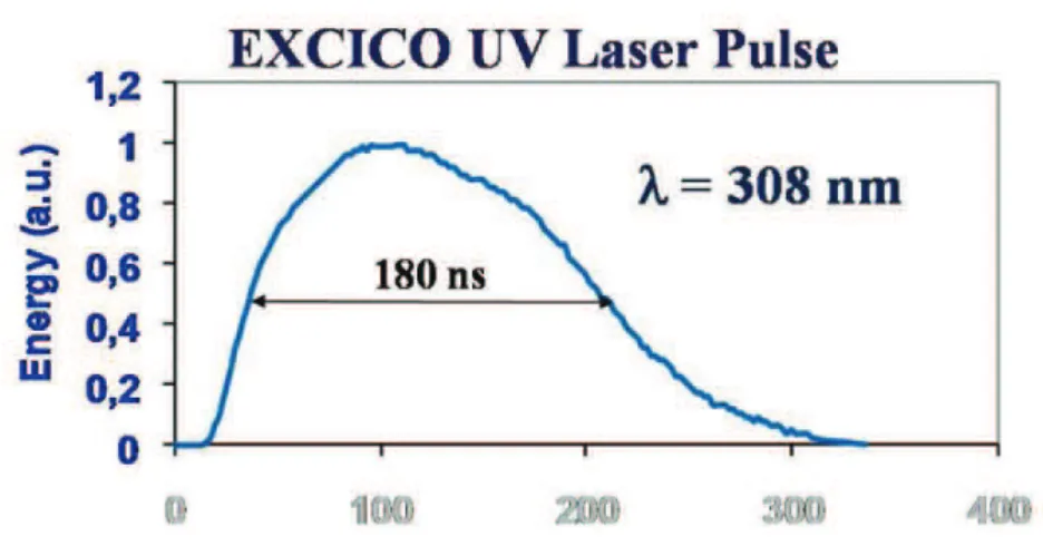
capacities of the electron and lattice subsystems, respectively, and λ a parameter characterizing the electron-lattice coupling in the target. Figure 1.2 shows the typical times for the scattering and recombina-tion processes in silicon as a funcrecombina-tion of electron density (left hand scale). The distances of the thermal diffusion at room temperature and the melting point are also reported (right hand scale). Being the atom mass too large to interact with the high frequency photons, a laser light interacting with an absorber releases its energy by means of the (valence) electron and phonon systems. This energy can be re-irradiated or transformed in heat. The conversion occurs by means of electron-phonon interactions or Auger recombination. If τeis of the
order of 1 ps and τl is of the order of ns or less (see blue and red line
of Figure 1.2), the electron absorbed energy has enough time to be transferred to the lattice.
Consequently, the electrons and the lattice reach thermal equilib-rium and heat conduction in the target can be described by means of Fourier’s law, provided that the heat flux is constant over several mean free paths of the electrons that carry the heat. In these
condi-1.3 The thermal problem for non-melting laser processes
Figure 1.2.: Time for scattering and recombination processes in sil-icon as a function of electron density (left). Distances of thermal diffusion at room temperature and the melting point (right). As ref-erence, the blue and red line indicate respectively, the typical time scale of an 180 ns excimer laser process and a millisecond continuous laser scanning.
tions, approximations can be done for the heat source. In turn, for irradiation pulses with duration less than one nanosecond, a model which considers explicitly the electron and lattice system has to be taken into account. The celebrated two-temperature model (TTM), developed by Anisimov et al. in 1974 [4], belongs to this model class. The second point to be considered is the interaction of the laser light with the irradiated structure at the laser wavelength scale. The lim-iting case, where these interactions do not play any role in the irra-diation, is that of a unique substrate with a thickness greater than its absorption length at the considered light frequency. In this case
we can implement the source in the heat equation in a easy way by means of the following equation
S(t, z) = I(1 − R) αe−αz (1.1) where I is the incident laser energy, R and α are the phase and tem-perature dependent surface reflectivity and the material absorption at the laser wavelength, respectively. In this form it gives the heat quantity absorbed by the irradiated sample at the time t and position
z in depth. If our simulation is 2 or 3 dimensional, than the laser
shape in the normal directions with respect to the laser beam has to be introduced by means of proper normalized functions. This kind of laser processes play a role only in the investigation of the direct or indirect effects of laser irradiation on particular materials.
Today laser processes involve very complex structures with a charac-teristic scale of the order of the laser wavelength. In particular we could refer to multilayer structures and patterned samples. In the first case a source like Equation 1.1 can be considered in the heat equation only if the component that rules the absorption in the bulk material (i.e. (1 − R) αe−αz) becomes negligible in the first irradiated
layer. If this condition it not verified we must consider multiple inter-nal reflections that occur in such structures, based on the assumption that light combines coherently (or incoherently in the case of a dis-ordered material) at each point in the layer under consideration. As a consequence the heat equation must be coupled with a proper code which calculates the real source, determining the optical absorption spectrum and optical absorption profile for any layer in the irradiated thin-film multilayer.
Concerning the laser irradiation of patterned structures, generally the problem lies on the interface where the interaction between the light and the periodic geometry of the integrated electronic devices has to be taken into account. In these conditions, a direct determination of the source starting from the numerical solution of the Maxwell equations is needed. They have to be solved in a box which mimics the real periodic structure.
1.3 The thermal problem for non-melting laser processes
In the following we will give the implementation details, presenting particular examples where the laser process simulations have sup-ported the process design. This work has been carried forward in collaboration with experimental teams during the Ph. D. activity. In this research, the support of the experimental analysis with com-puter simulation of the annealing process has been fundamental both in predicting the melting phenomenon and the temperature evolution with the aim to determine convenient process windows and, in gen-eral, bulk effects of the laser light. In particular, focusing on the heat problem and the simulation details, the case of the crystallization of implanted amorphous silicon during millisecond annealing by infrared laser irradiation will be described [57]. Moreover, irradiation effects on multi-layer structures with the related issues and solutions will be also discussed. Concerning laser irradiation of patterned structures in the melting regime, we remand the reader to the chapter 5, which deals in detail with the problem in 2 dimensions.
1.3.1. Cristallization of amorphus silicon by scanning millisecond laser annealing
One of the main advantages of amorphous Si (α-Si) compared to crys-talline Si (c-Si) is its production technique, as α-Si can be easily de-posited at very low cost. This advantage is paid in terms of worse electronic properties which are not sufficiently good in order to sat-isfy the increased performance requirements of fast electronic device. However, starting from a low cost α-Si substrate, polycrystalline sil-icon layer can be generated by means of solid phase epitaxy SPE [67], spontaneous crystallization [89], or excimer laser annealing [28]. Most of the studies concerning crystal grain nucleation and growth are based on the Avrami–Johnson–Mehl description under the hypothesis that the nucleation rate, abruptly approaches a constant steady state value after a given incubation time. The characteristic crystallization time, depends on the steady-state nucleation rate and grain growth velocity, and it is about 20 s at 780 °C. Higher temperature cannot be easily investigated, by rapid thermal annealing, because the nu-cleation rate and the growth velocity are so high that the sample is
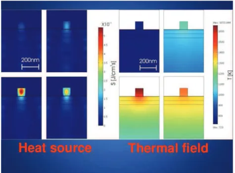
Figure 1.3.: Snapshots of the heat source (left side panels) and tem-perature (right side panels) during a 2 dimensional laser irradiation simulation of a real device structure.
crystalline already during the heating up. Hence, it arises the need of smaller annealing time scale.
In the work [57], Mannino et al. extended the description of the spontaneous crystallization up to 1323 K, i.e. 250 K above the tem-perature investigated by conventional annealing. In particular, we described the time evolution of the crystallized fraction during the infrared (IR) laser irradiation process of amorphous Si. A CW GaAs solid-state laser emitting at the wavelength of 808nm in the scanning configuration was used. The experimental equipment, by means of a fine tuning of the laser fluence and the scanning velocity, allows us to set the overall thermal budget supplied to the irradiated substrate. In order to reliably simulate the process, we have solved the time evo-lution of the nucleation rate following the theoretical model proposed
1.3 The thermal problem for non-melting laser processes
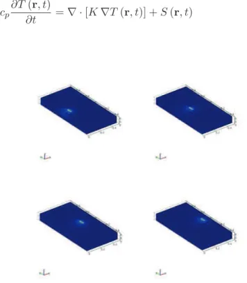
by Kelton et al. [42], based on the numerical solution of the system of coupled differential equations governing the time dependence of the Si cluster concentration. After a check and a calibration of the model for several conventional thermal processes given in ref. [89], we have coupled the nucleation model with the time-dependent thermal field solver developed by our theoretical group for the particular laser pro-cess considered. We have calculated the temperature profile induced by laser irradiation simulating the thermal field T( r,t) evolution dur-ing the laser scanndur-ing process. The heat equation
ρcp∂T (r, t)
∂t = ∇ · [K ∇T (r, t)] + S (r, t) (1.2)
Figure 1.4.: Snapshot sequence taken from the numerical simulation of heat diffusion equation, corresponding to four different times be-longing to the same process of continuous laser scanning. The sim-ulation refers to a laser scan with a velocity v = 7 cm/s and a power equal to P = 114.45 W.
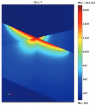
Figure 1.5.: Temperature field in the two perpendicular planes to the surface (xz and yx) of the crystal, which both pass through the spot center. The temperature is given in a color scale. The simulation refers to a laser scan with a velocity v = 7 cm/s and a power equal to P = 114.45 W.
has been solved in a three-dimensional computational box simulat-ing the sample with the proper temperature and space dependent thermal and optical properties [53]. We would like to stress that in Equation 1.2 the material density ρ, the heat capacity at constant pressure cp and the thermal conductivity K are temperature
depen-dent. The implemented values are listed on Table C.1 of Appendix C. The irradiation has been considered by means of a volume heat source, reproducing the spot characteristics in terms of power and space distri-bution, thus mimicking the relative motion between spot and sample. We have implemented the present and future PDE based continuum models and determined the corresponding numerical solutions in
dif-1.3 The thermal problem for non-melting laser processes
ferent conditions using the finite element COMSOL solver of differ-ential equations (Appendix A). Here, the main simulation difficulty (common with other irradiation processes discussed in this thesis) is related to the implicit dependence of the source on T. Indeed, apart from the usual variations with time and space, the heat source depends also self-consistently on the thermal field itself due to the dependence of the optical properties on T. As an example, we can observe in Figure 1.3 how the heat source changes during a laser irradiation pro-cess for a 2 dimensional simulation case. The four graphs are snap-shots of the heat source (left side panels) and temperature (right side panels) during the laser irradiation of a real device structure. In this case near field solutions of the Maxwell equations are necessary to quantitatively determine the heat source.
In the case of the crystallization experiment we can apply the simula-tion setting for the continuous wave irradiasimula-tion of plane samples which are homogeneous in depth in the light absorption region. Therefore, if we choose x as the scan direction and z the laser beam direction,
Figure 1.6.: Thermal field associated to a laser process with a scan-ning speed v = 7 cm/s and a power of P = 114.5 W. The plot shown is the temperature variation seen by a generic point on the surface as a function of time.
then the source term S (x, t) can be written as following:
S (x, t) = Φ (z) · F (x, y, t) , (1.3) where Φ (z)is the absorbed power density in the z direction, approxi-mated with the functional relation of Equation 1.1 where reflectivity and absorption length are T dependent expressions, and F (x, y, t) is a normalized function which describes the laser shape on the orthog-onal plane to the z direction of laser propagation. The experimental equipment allow to visualize and extract the x and y spatial distri-bution of the laser intensity. In our case, F (x, y, t) = G (x, t) · R (y) where G (x, t) and R (y) are, respectively, a gaussian and rectangular function.
Figure 1.4 shows the snapshot sequence taken from the numerical sim-ulation of heat diffusion equation, corresponding to four different times belonging to the same process of continuous laser scanning on a crys-talline silicon substrate. The simulation refers to a laser scan with a velocity v = 7 cm/s and a power equal to P = 114.45 W. Referring to the same laser process, Figure 1.5 and Figure 1.6 show, respectively, the space and temporal distributions of the temperature taken at the laser spot center (in a generic point on the surface during the constant velocity laser scan).
In the amorphous silicon case, the peak temperature estimated in one of the central points along the scanning direction [Figure 1.7(a)] is of 1323 K. Note that apart from two regions at the borders of the annealed samples the temperature pulse is similar for all these points. The results of Figure 1.7(b) have been obtained solving the coupling models for thermal field and nucleation evolution. Nucleation rate (full line) is significantly different from zero only after 12.5 ms when temperature reaches its maximum value (1323 K), then rapidly in-creases to a peak value of 3.5×1017 cm−3 s−1, and finally decreases
to zero in a time interval as short as 7 ms. In the meanwhile, the crystalline volume fraction χc [dashed line in Figure 1.7(b)]
1.3 The thermal problem for non-melting laser processes
Figure 1.7.: (a) Temperature profile reached by α-Si in the middle of the laser scan by thermal field evolution simulation, and (b) nu-cleation rate of crystalline grains in α-Si (full line) and crystalline volume fraction (dashed line) during the temperature profile in (a).
constant because grain growth velocity strongly reduces decreasing the temperature.
The results have demonstrated that a general model, not necessarily based on the assumption of a steady state, can be used to draw a consistent scenario of α-c phase transition occurring up to tempera-tures as high as 1323 K, i.e. about 250 K higher than that reachable by conventional annealing, for few milliseconds. This investigation has been made accessible thanks to the use of process simulation: the knowledge of the transient variation of the temperature during the laser irradiation, namely during the crystallization process has been fundamental in order to predict the correct nucleation rate. On the other hand, due to the time and space dependence of the heat source,
the access to this bulk thermal properties during the millisecond an-nealing process is only possible by means of the simulations, making them fundamental for the analysis and the investigation of the laser effects on the material modifications.
1.3.2. Irradiation of multi-layer structures
Electronic devices based on thin-film multi-layer structures have re-ceived a great interest in the last years. They find application in many areas as solar cells, data storage, light emission, light trapping devices and involve various materials like metals, semiconductors, ox-ide, chalcogenides or organics. Laser irradiation of these multi-layered structures can be used as a heat source achieving high process temper-ature in a short annealing time, which goes from millisecond (contin-uous scanning configuration) to nanosecond (pulsed laser irradiation). Generally the knowledge of the temperature as a time and space func-tion during the heating process as well as the determinafunc-tion of the process window for melting, partial melting or no-melting irradiation is vital. All these requests can be supplied by means of a simulation support as seen in the previous paragraph.
On the other hand, multi-layer structures introduce new difficulties on the heat source estimation. In fact, multi-layer systems are usu-ally composed by few nanometers thick films, i.e. critical dimensions of the order of the wave length of the used laser equipment. There-fore, simplified implementations of laser source on the heat equation which do not consider coherent (or incoherent) interference between light waves in the structure are totally wrong. Heat equation has to be coupled with a proper code which can calculate the real source, determining the optical absorption spectrum and optical absorption profile for any layer in the irradiated thin-film multilayer structure. In order to achieve this goal, we have developed a one-dimensional model which takes into account the multiple internal reflections that occur in such structures, based on the assumption that light combines coherently at each point of the layer under consideration. Without entering in the implementation details [76], considering an incident
1.3 The thermal problem for non-melting laser processes
Figure 1.8.: Absorption profile on the GST layer obtained with the matrix method for a wave length of 1064 nm (multilayer composed by: 50 nm GST, 550 nm SiO2, 690 μm c-Si).
wave monochromatic and incident normal to the front layer, the code calculates the reflected, transmitted and absorbed fractions of the elec-tromagnetic radiation intensity. Furthermore, the absorption profile on each single layer is determined as a function of the depth orthog-onal to the multilayer system. The data needed for the calculations are the complex index of refraction and the dimension of each layer of the system. The model is based on the solutions, derived by means of the matrix method, of the equations relating the four electromagnetic field amplitudes on either side of an interface.
As an example, we consider a multi-layer substrate formed by 50 nm of GST, 550 nm of SiO2 and 690 µm of c-Si. We have calibrated the code
with the known refractive index dependence of the different substances on the laser frequency. Considering that we irradiate the sample with a pulsed 12ns Nd:YAG monochromatic laser having a wave length of 1064 nm, the absorption profile can be calculated. Results suggest that only the GST layer absorbs the light, being the c-Si substrate almost transparent for the photon energy here considered (E1064=
1.16 eV). Figure 1.8 shows the results for the first 60 nm from the irradiated surface. As we can see, the coherent interference between light waves in the structure produces an absorption profile totally different from the simple exponential one
A(x) = α exp(−α · x) (1.4)
adopted for irradiation of single substrate with a thickness greater than the light absorption length. For the wave length of 1064 nm, the inverse of the absorption coefficient of GST is 1/αGST= 38 nm [46].
1.4. The melting problem
In the investigations of the material modifications due to the laser irradiation of a processed substrate it is fundamental to know the temperature distribution as well as the melting and solidification de-tails in the annealed regions. Since all these quantities are difficult to measure directly, a theoretical analysis of the problem by means of process simulations is a key point for the process control. In the last section we treated a laser irradiation process in a non-melting regime. Many experimental investigations lie on these conditions where mate-rial modifications due to laser irradiation play a role only in the solid phase and phase transitions do not occur.
However, interesting phenomena appear when the heat due to the ir-radiation melts the processed sample. Heat transfer in laser-induced melting and solidification is a transient, non-linear phenomenon with a moving solid/liquid interface corresponding to the release or ab-sorption of latent heat during phase change. In order to deal with phase change problems, many numerical methods such as front track-ing methods and fixed domain methods have been and are still be-ing developed. The main advantage of fixed domain methods [78] is that no explicit tracking of the phase front is needed. A number of fixed grid methods have been proposed including effective specific heat methods [36], enthalpy methods [20, 44], source term methods
1.4 The melting problem
[101] and phase field models [41, 104]. In the following, we will deal with the laser melting problem from the simulation point of view, giv-ing a description of the most common methods used. Firstly, a front tracking model for the resolution of the Stefan problem will be pre-sented. Afterwards, we will give details of two fixed domain methods, i.e. the enthalpy and the phase field methods. The latter two can be implemented in order to solve the thermal problem for laser irradiated substrates.
1.4.1. Front tracking model
Many relevant heat conduction or diffusion problems involve phase transformations. A common example of such a problem is the ice-melting one that was firstly treated by Stefan [90]. Thereon, these kind of problems are widely referred to as Stefan problems. During melting or solidification, the moving boundary (interface) separating the liquid and the solid phases of the material changes with time. In both sides of this interface, the classical heat equation is satisfied. On the solid/liquid interface, the released or absorbed latent heat is balanced with the heat fluxes from both phases.
In order to give an idea of how the front tracking model deals with Stefan problems, in the following we present a particular model for the case of melting evolution, i.e. solid liquid phase transformation. It is important to note that front tracking methods consider explicitly the solid-liquid interface as a variable of the problem to be determined. Let us consider a fixed domain [0, l], where we have a material that is in its liquid state in a certain region [0, s(t)] and in its solid state in the rest of the domain. The point separating the liquid and the solid phases determines the position of the interface s(t). We denote the temperature in the point x at time t by u(x, t). The governing equations for this problem are the heat equations in both the liquid and the solid phases
∂u ∂t(x, t) = ∂ ∂x 3 Kliq ∂u ∂x 4 , x ∈ Ωliq (1.5)
∂u ∂t(x, t) = ∂ ∂x 3 Ksol ∂u ∂x 4 , x ∈ Ωsol, (1.6)
where Ksol and Kliq denote the thermal diffusivities in the solid and
the liquid phase respectively, which involve the heat capacity, density and the heat conduction coefficient of the materials. The velocity v of the interface is given by the jump condition
Lv = Ksol
∂u
∂x(x, t) |x↓s(t)−Kliq ∂u
∂x(x, t) |x↑s(t), (1.7)
where L denotes the latent heat of solidification. This last equation is frequently called the Stefan condition. At the interface we have the melting temperature. Generally here it is chosen to be zero without loss of generality: u(s(t ), t) = 0. If the position of the interface s is a differentiable function, the velocity of the interface v can be replaced by L∂s ∂t(t) = Ksol ∂u ∂x(x, t) |x↓s(t) −Kliq ∂u ∂x(x, t) |x↑s(t). (1.8)
Subsequently boundary and initial conditions have to be fixed in order to have a unique solution.
1.4.2. Enthalpy model
Implicit or fixed domain methods are the natural alternative to front tracking methods. Within them the most used are the enthalpy method, the level set method and the phase field method. In the enthalpy method (ref. [18]) the enthalpy function is introduced. This function measures the total heat of the system, and it has a jump discontinuity at the interface given by the heat released (or absorbed) during the phase change. This discontinuity is helpful to determine
1.4 The melting problem
the interface position. In the following we will present an enthalpy formulation for the heating-melting problem in the case of laser irra-diation.
Heat conduction and phase changes in the target are ruled by the energy conservation law in terms of the (volumetric) enthalpy H
∂tH + ∇ · þQ = S . (1.9)
where þQ is the heat flux and S a possible heat source.
The energy conservation law directly updates the enthalpy H (per unit volume) to new times, from which we need to find the new phase, temperature and phase fractions. Therefore, in order to determine the temperature evolution, it has to be coupled with an appropriate equation for T. The Equations of State H = H(T, P, phase), con-sistent with the thermo-chemistry of the material, can support our request:
dHi= CpidT + [−αiT + 1]dP i = S, L, (1.10)
where Ci
p and αi are the heat capacity (per unit volume) and thermal
expansion coefficient of phase i, respectively. The enthalpy within each phase (Solid, Liquid) can be expressed in terms of the pair (T, P ) by integration along constant T and constant P paths on the (T, P )-phase diagram relative to a consistent reference state. Integration of Equation 1.10 for constant P paths can be coupled with Equation 1.9 for H evolution.
H denotes volumetric enthalpy (per unit of volume), lower case h
denotes specific enthalpy (per unit of mass). Clearly, H = ρh in each phase. The value href (and thus also Href = ρShref) of the enthalpy at
the reference state can be arbitrary. Since the heat capacity is strictly positive and ∆Hf us and ∆Hvap are also positive (by our choice of
href), the dependence of H on T is monotonic. Thus T can be found
from H.
1.4.3. Phase field methodology
The phase field approach has its roots in statistical physics. In par-ticular, a new thermodynamic variable is introduced, the phase field
φ(x,t), which is associated with the phase of the system as a function of the time and space and varies smoothly from one value in the liquid to another value in the solid across a spatially diffusive interface region of thickness W. The advantages of applying the phase-field methodol-ogy on phase transition problems are twofold: a) it provides a simple, elegant description that appears to embody a rich variety of realistic physical growth phenomena; b) from a computational point of view, it is in principle simple to obtain solutions since it is not necessary to distinguish between the different phases. These issues are important when solid or liquid regions change with time.
As for all the other thermodynamic variables, the Helmholtz free en-ergy F (ϕ, ...) is also a functional of the phase field and its gradient is in the following form:
F (ϕ, ...) = ˆ Ω 5 f (ϕ, ...) + 1 2ǫ 2(∇ϕ)2+ ...6dΩ, (1.11)
where Ω is the system domain, f(φ,...) the Helmholtz free energy density for a phase with no gradients (usually a “double-well” function of φ is chosen). The problem presented can be then formulated in terms of partial differential equations. The phase field is then assumed to evolve as · ϕ∝ L 3δF δϕ 4 , (1.12)
where L is some partial differential operator satisfying L (0) =0. This equation is then supplemented by partial differential equations for the other thermodynamic variables. We adopt the following phenomeno-logical free energy
F = ˆ Ω C f (ϕ) + [W (n)] 2 2 | → ∇ϕ |2 +bλu 2 2 D dΩ, (1.13)
1.4 The melting problem
where W is the interface thickness and n the normal direction to the interface n= → ∇ϕ |∇ϕ |→ . (1.14)
λ is a dimensionless parameter that controls the strength of the
cou-pling between the phase and diffusion fields (typically of order unity),
b a constant and u denotes the dimensionless temperature field
u = cp· (T − TM)
L . (1.15)
Here TM is the melting temperature, L the latent heat of melting and
cpthe specific heat at constant pressure. Applying a single Lyapounov
functional (expressed in the variational form), the basic equations of the phase-field model can be obtained:
τ (n)∂ϕ ∂t = − δF δϕ (1.16) ∂U ∂t = D bλ∇ 2δF δU, (1.17)
for the independent variables phase field φ and the dimensionless en-thalpy U defined by
U = u −h (ϕ)
2 . (1.18)
In the last equations, τ is the characteristic time of attachment of atoms at the interface (∼ 10-13 s for metallic systems), D the thermal
diffusivity and h(φ) is a function that describes the generation of latent heat. Equation 1.16 and Equation 1.17 imply that
dF
dt ≤ 0, (1.19)
if there are no fluxes across the boundaries of the volume where F is defined, i.e., the dynamics drives the system towards a minimum of free energy. To obtain a phase-field model that reduces to the desired free-boundary problem, it is generally sufficient to require that f(φ) has the shape of a double-well potential. The simplest choice for f(φ) that has been traditionally used is
f (ϕ) = −ϕ
2
2 +
ϕ4
4 . (1.20)
This last function has two local minima at ϕ = ±1, which correspond to the solid phase (φ = +1) and the liquid one (φ = -1). In order to ensure that a unit amount of latent heat is produced at the interface with the temperature field normalized by L / cp and for f(φ) defined
before, h(φ) has to satisfy the additional condition
h (+1) − h (−1)
2 = 1. (1.21)
Choosing g(φ) and h(φ) in a way that they satisfy the condition
g (ϕ) = b
2h (ϕ) , (1.22)
Equation 1.16 and Equation 1.17 reduce to the form
τ∂ϕ ∂t = W
2∇2ϕ − ∂F (ϕ, λu)
1.4 The melting problem ∂u ∂t = D∇ 2u +1 2 · ∂h (ϕ) ∂t , (1.24)
where F (ϕ, λu) = f (ϕ) + λg (ϕ) u is a function that has the form of a double-well potential where the relative height of the two minima is temperature dependent. However, it is important to stress that the constraint imposed by Equation 1.22 is not necessary to obtain phase-field equations that reduce to the desired free-boundary problem in the limit of a thin interface.
The following functional forms have been adopted for g(φ) and h(φ):
g (ϕ) = ϕ − 2ϕ 3 3 + ϕ5 5 (1.25) h (ϕ) = 15 8 A ϕ −2ϕ 3 3 + ϕ5 5 B , (1.26)
which satisfy Equation 1.22 with b = 16/15. Putting all the defined functions on Equation 1.16 and Equation 1.17 (or Equation 1.23 and Equation 1.24), we obtain the final phase field for the independent variables φ and T τ∂ϕ ∂t = W 2∇2ϕ − ϕ1 ϕ2− 12− λ cp Lf us (T − TM) 1 ϕ2− 122 (1.27) ρcp ∂T ∂t − ∇ 2(KT ) = ρLf us 2 15 8 1 ϕ2− 12∂ϕ ∂t + S (x, t) . (1.28)
where Lfus is the latent heat of the crystalline substrate, respectively.
The laser source term S, at time t and position z, is given by
where Elas is the incident laser energy, P(t) is the normalized laser
pulse shape, and R and α are the phase and temperature dependent surface reflectivity and the material absorption at the laser wave-length, respectively.
Since the melt thickness is very small, convective effects do not arise in the melt. Thus the heat flux in the solid and liquid is due to heat conduction only, þQ = −k∇T , with k = thermal conductivity, T =
temperature. On the contrary, the presence of strong advection in the plume domain requires solution of the continuity and momentum equations as well.
All the material properties (heat capacity cp, heat conductivity K,
and density ρ) are phase and temperature dependent. The phase field parameters (τ, W, and λ) are chosen in order to correctly achieve the thin interface limit [41]. The phase field model calibration of parameters used in this work is equivalent to that reported in Ref. [49].
1.5. The challenge to activate implanted dopant
atoms by laser annealing
Laser Thermal Annealing (LTA) receives a great interest in the for-mation of ultrashallow junctions essential in nanoscale metal-oxide-semiconductor technology [2, 35, 70, and references therein]. A se-quence of ion implantation and thermal processing is commonly used to modify the electronic properties of semiconductors, in particular to create a space dependent work function in the material. Samples can be processed with laser irradiation for two reasons (sometimes concurrent): a) melt the near surface irradiated regions causing a re-distribution of the dopant atoms, an annihilation of the implant damage in the molten regions and a crystal regrowth; b) recovering implantation damage, activating and redistributing by diffusion the doping impurities in the solid phase.
As an example, we would like to report two experimental investiga-tions which consider dopant evolution in crystalline silicon substrate.
1.5 The challenge to activate implanted dopant atoms by laser annealing
Following the organization of the present chapter, first the evolution of a dopant B-delta layers under a millisecond laser annealing in a scanning configuration is described. Subsequently we will deal with dopant evolution in a double implanted silicon sample under pulsed nanosecond laser irradiation, where melting and non-melting condi-tions occur.
1.5.1. Dopant evolution in the millisecond scale
The non-equilibrium kinetics of a coupled system of point defects and impurities in Si has attracted a broad interest in the last decades. The past interest essentially focused in the non-equilibrium caused by a point defect excess and in the role played by this excess in the transient enhanced diffusion (TED) phenomena in Si. As a conse-quence, being the defect super-saturation the only relevant driving force of the non-equilibrium kinetics, the different stages (diffusion, aggregate nucleation, formation and annihilation of extended defects) of the defect evolution in Si at quasi-constant temperature are now well known. Moreover, a consistent modeling approach has been de-rived and validated by experimental works [30, 71, 91]. The current trend of the dopant activation process in Si is characterized by an extreme reduction of the annealing time (from the ms to ns regime for the ultra-fast thermal processes) and a correspondent increase of the peak temperature, eventually using the laser irradiation (LI) as a heat source [49, 50, 70, 105]. These processes should complement or substitute the actual rapid thermal annealing in the activation module of future nanoelectronics devices.
However, the post-implant kinetics of the defects–dopant system in the extremely far-from-the equilibrium conditions caused by the laser ir-radiation both in the non-melting and melting regime is almost totally unknown. From the theoretical point of view some relevant questions have to be addressed: the formalization of a reliable kinetic formalism for the evolving defect-impurity system in a non-uniform fast-varying thermal field, the generalization of the kinetic parameters (e.g. diffu-sivity, clustering rate constants, etc.) in this regime, the inclusion in the formalism of eventual phase transitions [49], the interaction
be-tween the defects generated by the implant and the defects generated by the process [52].
In order to clarify all these issues, different experimental and theoret-ical studies have been carried out. In particular, we have investigated dopant-defect system evolution on the millisecon scale [53].
The experiments have been performed on silicon samples containing chemical vapor deposition grown B-delta layers. The samples were implanted with Si ions to a dose of 5×10¹³ atoms/cm2 at an energy of 40 keV. Subsequent laser irradiations were performed using the GaAs solid-state laser which emitted a continuous radiation at the wavelength of 808 nm in the scanning configuration (same laser of subsection 1.3.1). Different annealing conditions have been investi-gated varying the velocity and the power of the laser beam. Experi-mental chemical profile before and after irradiation was performed by means of Secondary Ion Mass Spectroscopy (SIMS, see Appendix B for details).
Our investigation is focused on the effect of the Si interstitial super-saturation due to the Si ions implant on the substitutional dopant atoms of the B-delta layers. We arrange this particular experiment instead of a common dopant implant, in order to decouple Si inter-stitials with respect to the dopant atoms, preventing the formation of immobile dopant aggregates. In order to better understand the role of the silicon interstitial supersaturation on the dopant evolution, a substrate containing a B-delta layer has been annealed without a Si ion implant.
Solving the heat equation (simulation details are given in subsection 1.3.1), the temperature evolution in the whole irradiated substrate can be de-termined. Figure 1.4, Figure 1.5 and Figure 1.6 refer to the thermal problem of the laser annealing process here discussed. Concurrently a proper model for the dopant-defect system has been implemented. It is derived from the kinetic Boltzmann’s formalism. The model will be described accurately in subsection 2.4.2 and subsection 3.3.3. One of the results of our investigation is reported in Figure 1.9, where we compare the experimental (blue line) and simulated chemical boron profiles after an irradiation process carried out with laser scanning
1.5 The challenge to activate implanted dopant atoms by laser annealing
Figure 1.9.: Comparing the experimental (blue line) and simulated chemical boron profiles after an irradiation process carried out with laser scanning speed v = 7 cm/s and power P = 114.45 W. Th dark line refers to the as-grown B-delta layer.
speed v = 7 cm/s and power P = 114.45 W. The dark line refers to the as-grown B-delta layer. The temperature distribution associ-ated to this laser process seen by a generic point on the surface as a function of time is shown in Figure 1.6. An almost perfect agreement can be found between the experimental and simulated data. On the other hand, samples annealed without the Si implant do not show any substantial dopant diffusion. These results allow us to conclude that the defect system rules dopant evolution also at the millisecond scale. An application of the kinetic theory to the analysis of scanning laser processes seems to indicate that the relaxation time of the energy is much smaller than the thermal pulses (lasting fewtens of millisecond). Therefore, a unique local temperature can be used in the case of such thermal process. A noteworthy result of the analysis presented here is the confirmation of the reliability, in the case the laser scanning pro-cesses, of the energetic calibration for the I-type defects [30, 71, 91], derived with the aid of experiments based on standard thermal
an-nealing. This fact indicates that the energetic related to the stability of the complexes is (as we should expect) an intrinsic property of the system.
Millisecond laser irradiation causes non-equilibrium dopant diffusion. The scenario is totally different in the nanosecond scale, where dopant diffusion does not take place even for the high defect supersatura-tion here considered. Therefore dopant activasupersatura-tion remains the unique physical observable quantity (i.e. a quantity showing a kinetic trend) which allows a possible investigation of damage evolution in the sub-microsecond regime.
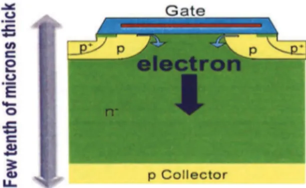
Figure 1.10.: Current IGBT Structure. Electrons move from the device top side to the collector.
1.5.2. Melting and non-melting dopant evolution for pulsed nanosecond irradiation
In order to report a real case where LTA can help the development of ultrashallow junctions, we would like to present in this sub-section a possible technological application. Power devices and particularly In-sulated Gate Bipolar Transistors (IGBT) are today a major part of the semiconductor market breakdown with a large range of device types in both consumer and industrial applications. Basically, IGBTs work as

![Table 2.2.: Cluster parameters implemented in the PDE model and KMC code (see chapter 4) for the dopant-defect system evolution [30, 37].](https://thumb-eu.123doks.com/thumbv2/123dokorg/4518183.34813/64.892.293.621.204.440/table-cluster-parameters-implemented-chapter-dopant-defect-evolution.webp)