PhD Thesis in Energy, Eng. A. Calabrese 1
T
ABLE OF CONTENTS TABLE OF CONTENTS... 1 LIST OF TABLES... 5 LIST OF FIGURES... 6 INTRODUCTION... 12 OUTLINE... 12 REFENENCES... 13 1 ORGANIC SEMICONDUCTORS... 14 1.1 INTRODUCTION... 14 1.2 CONJUGATED POLYMERS... 15 1.2.1 CHEMICAL STRUCTURE... 16 1.2.2 OPTICAL PROPERTIES... 19 1.2.3 ELECTRICAL PROPERTIES... 211.2.4 CHARGE CARRIERS TRANSPORT... 24
1.3 REFERENCES... 25
2 ORGANIC SOLAR CELLS... 28
2.1 INTRODUCTION... 28
2.2 BRIEF HISTORY... 29
2.3 OPERATING PRINCIPLES... 31
2.4 DEVICE PHYSICS... 34
2.4.1 PHOTON ABSORPTION AND EXCITON GENERATION... 34
2.4.2 EXCITON DIFFUSION... 35
2.4.3 EXCITON SEPARATION AND CHARGE CARRIER GENERATION... 36
2.4.4 CARRIER DIFFUSION TO THE ELECTRODES... 37
2.4.5 CHARGE-CARRIERS COLLECTION AT THE ELECTRODES... 38
PhD Thesis in Energy, Eng. A. Calabrese
2
2.5.1 SINGLE LAYER DEVICES... 39
2.5.2 BILAYER HETEROJUNCTION DEVICES... 40
2.5.3 BULK HETEROJUNCTION DEVICES... 41
2.6 CHARACTERIZATION OF A SOLAR CELL DEVICE... 43
2.7 CRITICAL PARAMETERS FOR SOLAR CELL EFFICIENCY... 45
2.7.1 OPEN CIRCUIT VOLTAGE... 45
2.7.2 SHORT CIRCUIT CURRENT... 46
2.7.3 FILL FACTOR... 47
2.8 REFERENCES... 49
3 MOTIVATION AND AIM... 52
3.1 INTRODUCTION... 52
3.2 LIMITS OF STATE OF THE ART ORGANIC SOLAR CELLS... 52
3.2.1 LIGHT ABSORPTION... 52
3.2.2 ENERGY LEVELS ALIGNMENT... 54
3.2.3 CHARGE TRANSPORT AND RECOMBINATION... 55
3.2.4 CHARGE EXTRACTION... 55 3.3 NEW MATERIALS... 56 3.4 AIM OF RESEARCH... 58 3.5 REFERENCES... 59 4 CHARACTERIZATION METHODS... 63 4.1 INTRODUCTION... 63
4.2 PHOTOPHYSICAL, CHEMICAL AND STRUCTURAL ANALYSIS... 64
4.2.1 NUCLEAR MAGNETIC RESONANCE SPECTROSCOPY... 64
4.3 UV-VIS SPECTROSCOPY... 65
4.3.1 THE IMPORTANCE OF CONJUGATION... 68
4.4 CYCLIC VOLTAMMETRY... 70
4.5 RAMAN AND FT-IR SPECTROSCOPY... 71
4.5.1 VIBRATIONAL SPECTROSCOPY ON CONJUGATED POLYMER... 72
4.6 MOLECULAR WEIGHT DETERMINATION... 74
4.6.1 GEL PERMEATION CHROMATOGRAPHY... 75
PhD Thesis in Energy, Eng. A. Calabrese
3
4.8 MORPHOLOGICAL STUDY... 77
4.9 TRANSPORT PROPERTIES INVESTIGATION... 80
4.10 DEVICE CHARACTERIZATION... 82
4.11 REFERENCES... 83
5 RESULTS AND DISCUSSION... 85
5.1 SYNTHESIS OF POLYMERS... 85
5.2 STRUCTURAL PROPERTIES... 88
5.3 VIBRATIONAL PROPERTIES... 89
5.4 OPTICAL PROPERTIES... 91
5.5 DETECTION OF CHARGE TRANSFER BY PHOTOLUMINESCENCE QUENCHING... 103
5.6 ELECTROCHEMICAL PROPERTIES... 106
5.7 INVESTIGATION OF CHARGE TRANSFER BY EPR SPECTROSCOPY... 108
5.7.1 TR-EPR SPECTRA ANALYSIS PERFORMED ON PRISTINE POLYMERS... 108
5.7.2 TR-EPR SPECTRA ANALYSIS ON POLYMERS BLENDED WITH FULLERENE... 113
5.7.3 LEPR SPECTRA ANALYSIS ON SOLID MIXTURES OF POLYMERS/PCBM ... 120
5.8 MODELLING... 128
5.8.1 COMPUTATION METHOD... 128
5.8.2 MODEL OPTIMIZATION... 129
5.8.3 TERMINAL SEQUENCES... 134
5.8.4 SPECULATIONS ON THE THEORETICAL RESULTS... 135
5.9 MOBILITY... 140 5.10 PHOTOVOLTAIC APPLICATIONS... 143 5.11 REFERENCES... 148 6 CONCLUSIONS... 150 7 EXPERIMENTAL... 155 7.1 MATERIALS... 155 7.2 SYNTHESIS... 155
7.2.1 LOW WEIGHT POLYMERS... 155
7.2.2 HIGH WEIGHT POLYMERS... 157
PhD Thesis in Energy, Eng. A. Calabrese 4 7.2.4 REFERENCE COPOLYMERS... 158 7.3 MEASUREMENTS... 159 7.4 REFERENCES... 162 APPEND A ... 163
PhD Thesis in Energy, Eng. A. Calabrese
5
L
IST OFT
ABLESTABLE 4.1TERMINOLOGY FOR ABSORPTION SHIFTS. ... 69
TABLE 5.1WEIGHT-AVERAGE MOLECULAR WEIGHT (MW), AND POLYDISPERSITY INDICES (PDIS) OF ALL COPOLYMERS... 87
TABLE 5.2ELEMENTAL ANALYSIS OF COPOLYMERS AT DIFFERENT STAGES OF PURIFICATION... 88
TABLE 5.3UV-VIS DATA OF P1-P4 COPOLYMERS WITH HIGH MOLECULAR WEIGHT, IN CHCL3 SOLUTION AND IN THIN FILM... 102
TABLE 5.4ELECTROCHEMICAL DATA OF P1-P4 COPOLYMERS. ... 106
TABLE 5.5ZFS VALUES AND POPULATIONS OF THE TRIPLET OF THE ALTERNATING COPOLYMER P4... 110
TABLE 5.6ZFS VALUES AND POPULATIONS OF THE TRIPLET OF THE RANDOM COPOLYMER P1. ... 110
TABLE 5.7ZFS VALUES AND POPULATIONS OF THE TRIPLET OF THE RANDOM COPOLYMER P2. ... 111
TABLE 5.8ZFS VALUES AND POPULATIONS OF THE TRIPLET OF THE RANDOM COPOLYMER P3. ... 112
TABLE 5.9CALCULATED ENERGY LEVELS OF SUBSTITUTED FLUORENE... 130
TABLE 5.10CALCULATED ENERGY LEVELS OF B, T AND F MONOMER UNIT... 130
TABLE 5.11CALCULATED STRUCTURAL DATA AND ENERGY LEVELS OF DIMERS. ... 131
TABLE 5.12CALCULATED ENERGY LEVELS OF TETRAMERS... 131
TABLE 5.13CALCULATED ENERGY LEVELS OF OCTAMERS... 132
TABLE 5.14CALCULATED ENERGY LEVELS OF THE ESADECAMERS... 134
TABLE 5.15OPTICAL ENERGY GAP VERSUS CALCULATED ENERGY GAP... 137
TABLE 5.16CALCULATED ENERGY GAP FROM THE MORE REPRESENTATIVE SET OF OCTAMERS AND COMPARISON WITH THE ELECTROCHEMICAL DATA. ... 138
TABLE 5.17CALCULATED ENERGY GAP FROM THE MORE REPRESENTATIVE SET OF TETRAMERS AND COMPARISON WITH THE ELECTROCHEMICAL DATA. ... 139
PhD Thesis in Energy, Eng. A. Calabrese
6
L
IST OFF
IGURESFIGURE 1.1OVERLAP OF HYDROGEN ATOM ORBITALS TO FROM BONDING AND ANTIBONDING ORBITALS. ... 16
FIGURE 1.2CONDUCTING CONJUGATED POLYMERS: ETHYLENE (C2H4). (A) TOP (B) FRONT (C) BONDING. THE SP2 HYBRID ORBITALS ARE SHOWN IN PURPLE, AND THE UNHYBRIDIZED PZ ORBITALS IN BLUE. ELECTRONS ARE REPRESENTED BY THE DOTS... 17
FIGURE 1.3ENERGY LEVEL IN ORGANIC SEMICONDUCTORS. ... 18
FIGURE 1.4MOLECULAR STRUCTURES OF SEVERAL COMMON CONJUGATED POLYMERS: POLY(ACETYLENE) (PA), POLY(THIOPHENE) (PT), POLY(PYRROLE) (PPY), POLY(PPHENYLENE) (PPP), POLY(P-PHENYLENEVINYLENE) (PPV) AND POLY(FLUORENE) (PF). ... 18
FIGURE 1.5SCHEMATIC DRAWING OF COMMON PHOTOPHYSICAL PROCESSES FOR A CONJUGATED MOLECULE OR POLYMER... 21
FIGURE 1.6CHANGE OF GEOMETRIC STRUCTURE OF POLYTHIOPHENE UPON DOPING... 22
FIGURE 2.1GENERAL MECHANISM FOR PHOTOENERGY CONVERSION IN ORGANIC SOLAR CELLS... 33
FIGURE 2.2 SCHEMATIC DIAGRAM OF A SINGLE LAYER DEVICE... 39
FIGURE 2.3 SCHEMATIC DIAGRAM OF A BILAYER HETEROJUNCTION AND SUBSEQUENT PHOTOINDUCED ELECTRON TRANSFER AT THE INTERFACE OF THE TWO LAYERS (P3HT/PCBM AS AN EXAMPLE)... 40
FIGURE 2.4 SCHEMATIC OF A BULK HETEROJUNCTION DEVICE. THE DONOR (D) IS BLENDED WITH THE ACCEPTOR (A) THROUGHOUT THE WHOLE FILM. ... 42
FIGURE 2.5FROM LIGHT ABSORPTION TO PHOTOCURRENT IN A BHJ SOLAR CELL.UP: SIMPLIFIED ENERGY DIAGRAM (1) SINGLET EXCITON GENERATION FROM AN ABSORBED PHOTON IN THE DONOR MATERIAL, (2) EXCITON DIFFUSION TO THE ACCEPTOR INTERFACE, (3) EXCITON DISSOCIATION BY ELECTRON TRANSFER TO THE ELECTRONEGATIVE ACCEPTOR MOLECULES, (4) CHARGE TRANSPORT OF ELECTRON RESP. HOLE BY HOPPING BETWEEN LOCALIZED STATES, (5) EXTRACTION OF THE CHARGES: PHOTOCURRENT.DOWN: FROM A KINETIC POINT OF VIEW. ... 43
FIGURE 2.6SCHEMATIC DIAGRAM OF I-V CHARACTERISTICS OF A PHOTOVOLTAIC CELL IN THE DARK (DARK) AND UNDER ILLUMINATION (RED) IN WHICH ARE REPRESENTED VOC,JSC, THE MAXIMUM POWER POINT, AND THE FILL FACTOR WHICH CAN BE REGARDED AS THE RATIO OF THE COLORED RECTANGLE AND LARGER UNCOLORED RECTANGLE. ... 45
PhD Thesis in Energy, Eng. A. Calabrese
7
FIGURE 3.1AM1.5 SOLAR SPECTRUM (DIRECT + CIRCUMSOLAR, AFTER ASTMG173). THE ABSORPTION SPECTRUM OF THE COMMONLY USED ABSORBER MATERIAL FOR BULK HETEROJUNCTION SOLAR CELLS, P3HT, IS INCLUDED FOR COMPARISON... 53
FIGURE 3.2CHEMICAL STRUCTURES OF SOME ALTERNATING PFO POLYMERS... 58
FIGURE 4.1 NONEXHAUSTIVE LIST OF INVESTIGATION TECHNIQUES REQUIRED FOR AN EXTENDED
CHARACTERIZATION OF ACTIVE MATERIALS FOR POLYMER (ORGANIC) SOLAR.CELLS. ... 64
FIGURE 4.2SCHEMATIC REPRESENTATION OF ORBITAL ENERGY LEVEL... 66
FIGURE 4.3ENERGY LEVELS DIAGRAM OF ETHANE, BUTA-1,3-DIENE, HEXA-1,3,5-TRIENE... 69 FIGURE 4.4 (A) A TYPICAL SOLAR CELL STRUCTURE CONSISTING OF PEDOT:PSS DEPOSITED ONTO A GLASS/ITO SUBSTRATE. THE PHOTOACTIVE LAYER IS SPUN CAST ATOP THE PEDOT:PSS FILM, FOLLOWED BY THE ALUMINUM CATHODE ELECTRODE EVAPORATION. (B) TOPOGRAPHIC IMAGE OBTAINED USING ATOMIC FORCE MICROSCOPY SHOWING PHASE SEPARATION WHERE YELLOW AND PURPLE AREAS ARE DONOR AND ACCEPTOR PHASES, RESPECTIVELY. A NANOSCALE PHASE SEPARATION OF DONOR AND ACCEPTOR MATERIALS IN THE ACTIVE LAYER IS NEEDED TO ACHIEVE EFFICIENT EXCITON DISSOCIATION AND CHARGE TRANSPORT. ... 78
FIGURE 4.5EXPERIMENTAL TECHNIQUES USED TO DETERMINE CHARGE CARRIER MOBILITY. CELIV: CHARGE
EXTRACTION BY LINEARLY INCREASING VOLTAGE; DI SCLC: DARK INJECTION SPACE CHARGE LIMITED CURRENT; TR-EL: TRANSIENT ELECTROLUMINESCENCE... 80
FIGURE 4.6 THE PULSE SEQUENCE AND SCHEMATIC RESPONSE OF THE TOF, CELIV AND PHOTO-CELIV
TECHNIQUE. THE CALCULATION OF MOBILITY AND THE TYPICAL THICKNESS OF THE DEVICE ARE ALSO DISPLAYED FOR COMPARISON... 81
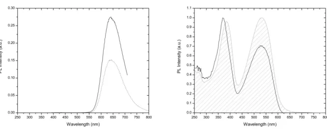
FIGURE 5.2NORMALIZED UV-VIS ABSORPTION SPECTRA OF P4 COPOLYMER IN CHCL3 SOLUTION (SOLID)
AND IN THIN FILM (DOT). ... 92
FIGURE 5.3LEFT: NORMALIZED PL SPECTRA OF P4 WITH EXC=384 NM (SOLID LINE) AND EXC=532 NM
(DOT LINE). RIGHT: NORMALIZED PL SPECTRUM OF P4 MEASURED AT MAXIMUM PHOTOLUMINESCENCE YIELD (MAX=640 NM). GREY PATTERNED AREA REPRESENTS THE ABSORPTION SPECTRUM IN ARBITRARY
UNITS. ... 94
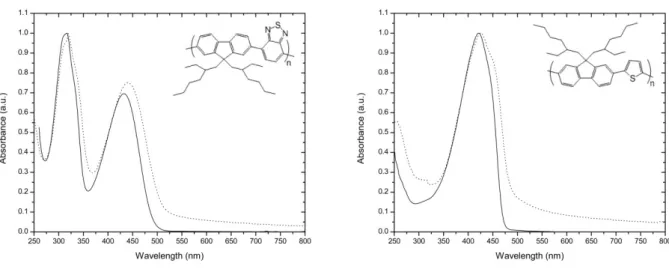
FIGURE 5.4NORMALIZED UV-VIS ABSORPTION SPECTRA OF (F-B)N (LEFT) AND (F-T)N (RIGHT) COPOLYMERS
PhD Thesis in Energy, Eng. A. Calabrese
8
FIGURE 5.5LEFT:NORMALIZED PL SPECTRUM OF F-B COPOLYMER IN THIN FILM WITH EXC=440 NM.RIGHT:
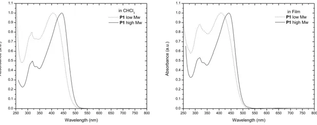
NORMALIZED PL SPECTRUM OF F-T COPOLYMER IN THIN FILM WITH EXC=425 NM. ... 95 FIGURE 5.6NORMALIZED UV-VIS ABSORPTION SPECTRA OF COPOLYMER P1 IN CHCL3 SOLUTION (LEFT) AND
IN THIN FILM (RIGHT)... 96 FIGURE 5.7NORMALIZED UV-VIS SPECTRUM OF RANDOM COPOLYMER P1(SOLID LINE)COMPARED TO THE SPECTRUM OF THE LINEAR COMBINATION OF ALTERNATING POLYMER F-B AND F-T SPECTRA (DOT LINE), BOTH REGISTERED IN CHCL3 SOLUTION. ... 97 FIGURE 5.8NORMALIZED PL SPECTRA OF LOW MW P1 IN THIN FILM WITH EXC=415 NM (DOT LINE) AND
HIGH MW P1 IN THIN FILM WITH EXC=450 NM (SOLID LINE). ... 98 FIGURE 5.9NORMALIZED UV-VIS ABSORPTION SPECTRA OF COPOLYMER P2 IN CHCL3 SOLUTION (LEFT) AND
IN THIN FILM (RIGHT)... 99 FIGURE 5.10NORMALIZED UV-VIS SPECTRUM OF HIGH MW P2 COMPARED TO THE UV-VIS SPECTRUM OF P4, BOTH ACQUIRED ON THIN FILM. ... 100
FIGURE 5.11NORMALIZED PL SPECTRUM OF HIGH MW P2 WITH EXC=550 NM (SOLID LINE) COMPARED TO
THE PL SPECTRUM OF P4 EXC=532 NM (DOT LINE), BOTH ACQUIRED ON THIN FILM. ... 101 FIGURE 5.12 NORMALIZED UV-VIS SPECTRA OF P3 IN THIN FILM FROM CHLOROFROM (SOLID LINE), O-DICHLOROBENZENE (DASH LINE), CYCLOHESANE (DOT LINE)... 102
FIGURE 5.13PL SPECTRA OF PRISTINE FILM P4 (SOLID LINE) AND OF P4 BLENDS WITH PCBM (1:0.1 W/W)
(DASH LINE), (1:0.5 W/W) (DOT LINE), (1:1 W/W) (DASH DOT LINE) WITH EXC=460 NM. FOR
CONVENIENT, THE INTENSITY OF BLENDS IS AMPLIFIED OF A FACTOR 5. ... 104
FIGURE 5.14PL SPECTRA OF PRISTINE FILM P1 (SOLID LINE) AND OF P1 BLENDS WITH PCBM (1:0.1 W/W)
(DASH LINE), (1:0.5 W/W) (DOT LINE), (1:1 W/W) (DASH DOT LINE) WITH EXC=460 NM. FOR
CONVENIENT, THE INTENSITY OF BLENDS IS AMPLIFIED OF A FACTOR 5. ... 105
FIGURE 5.15PL SPECTRA OF PRISTINE FILM P2 (SOLID LINE) AND OF P2 BLENDS WITH PCBM (1:0.1 W/W)
(DASH LINE), (1:0.5 W/W) (DOT LINE), (1:1 W/W) (DASH DOT LINE) WITH EXC=460 NM. FOR
CONVENIENT, THE INTENSITY OF BLENDS IS AMPLIFIED OF A FACTOR 5. ... 105
FIGURE 5.16VOLTAMMOGRAMS OF P1-P4 COPOLYMERS WITH HIGH MW AFTER PURIFICATION PROCESS.
PhD Thesis in Energy, Eng. A. Calabrese
9
FIGURE 5.17LEFT:TR-EPR DATASET (INTENSITY VS.FIELD / TIME) OF P4 IN O-DCB SOLUTION.RIGHT: TR-EPR SPECTRUM EXTRACTED AT TIME T = 0.5 MICROSECONDS (RED CURVE) AND ITS SPECTRAL SIMULATION (BLACK CURVE). ... 109
FIGURE 5.18TR-EPR SPECTRUM OF P1 EXTRACTED AT TIME T =0.5 MICROSECONDS (RED CURVE) AND ITS SPECTRAL SIMULATION (BLACK CURVE). ... 110
FIGURE 5.19LEFT:TR-EPR DATASET (INTENSITY VS.FIELD / TIME) OF P2 IN O-DCB SOLUTION.RIGHT: TR-EPR SPECTRUM EXTRACTED AT TIME T = 0.5 MICROSECONDS (RED CURVE) AND ITS SPECTRAL SIMULATION (BLACK CURVE). ... 111
FIGURE 5.20LEFT:TR-EPR DATASET (INTENSITY VS.FIELD / TIME) OF P3 IN O-DCB SOLUTION.RIGHT: TR-EPR SPECTRUM EXTRACTED AT TIME T = 0.5 MICROSECONDS (RED CURVE) AND ITS SPECTRAL SIMULATION (BLACK CURVE). ... 112
FIGURE 5.21JABLONSKY DIAGRAM DESCRIBING THE EXCITED STATE OBSERVED BY TR-EPR. ... 113 FIGURE 5.22LEFT TR-EPR DATASET (INTENSITY VS. FIELD / TIME) OF THE BLEND P4/PCBM (1:1 W/W) ON FILM FROM O-DCB. RIGHT :TR-EPR SPECTRUM EXTRACTED AT TIME T = 0.5 MICROSECONDS OF PCBM (BLACK CURVE), P4 (RED CURVE) AND P4/PCBM (RED CURVE)... 114
FIGURE 5.23TR-EPR SPECTRUM EXTRACTED AT TIME T = 10 MICROSECONDS OF PCBM (BLACK CURVE) AND P4 (RED CURVE) IN FROZEN MATRIX AND P4/PCBM (RED CURVE) ON FILM (RIGHT)... 115 FIGURE 5.24JABLONSKI DIAGRAM DESCRIBING THE BLEND P4/PCBM PHOTOPHYSICS. ... 115 FIGURE 5.25LEFT: TR-EPR DATASET (INTENSITY VS. FIELD / TIME) OF THE BLEND P1/PCBM (1:1 W/W) ON FILM FROM O-DCB. RIGHT:TR-EPR SPECTRUM EXTRACTED AT TIME T = 0.5 MICROSECONDS OF PCBM (BLACK CURVE), P4 (RED CURVE) AND P4/PCBM (RED CURVE)... 116
FIGURE 5.26EPR SPECTRUM EXTRACTED AT TIME T = 0.5 MICROSECONDS OF THE BLEND P1/PCBM (1:1
W/W) ON FILM FROM O-DCB AT DIFFERENT TEMPERATURES. ... 116
FIGURE 5.27JABLONSKI DIAGRAM DESCRIBING THE BLEND P1/PCBM PHOTOPHYSICS. ... 117
FIGURE 5.28LEFT: TR-EPR DATASET (INTENSITY VS. FIELD / TIME) OF THE BLEND P2/PCBM (1:1 W/W) ON FILM FROM O-DCB. TR-EPR SPECTRUM EXTRACTED AT TIME T = 0.5 MICROSECONDS (RED CURVE), AT TIME T = 10 MICROSECONDS (BLUE CURVE) AND THE SPECTRUM OF P2 IN FROZEN MATRIX (BLACK CURVE). ... 117
PhD Thesis in Energy, Eng. A. Calabrese
10
FIGURE 5.30LEFT:TR-EPR DATASET (INTENSITY VS.FIELD / TIME) OF THE BLEND P3/PCBM(1:1 W/W) ON FILM FROM O-DCB. RIGHT:TR-EPR SPECTRUM EXTRACTED AT TIME T = 0.5 MICROSECONDS (RED CURVE), AT TIME T = 12 MICROSECONDS (BLUE CURVE) AND P3/PCBM (BLACK CURVE)... 118
FIGURE 5.31JABLONSKI DIAGRAM DESCRIBING THE BLEND P3/PCBM PHOTOPHYSICS. ... 119 FIGURE 5.32SCHEMATIC DIAGRAM OF POSSIBLE ARRANGEMENTS OF ENERGY LEVELS OF A POLYMER/PCBM
AND RELATED EFFICIENT PHOTOPHYSICAL PROCESSES (ELECTRON TRANSFER PET AND / OR RECOMBINATION) IN THIS SYSTEM DEPENDING ON THE ENERGY INVOLVED.S1 AND T1 IN THE DIAGRAM REPRESENT THE EXCITED SINGLET AND TRIPLET OF THE POLYMER AND / OR PCBM, CT IS THE TORQUE GENERATED BY ELECTRONIC TRANSFER... 120
FIGURE 5.33LESR SPECTRA OF THE BLEND P4/PCBM (1:1 W/W) ON FILM FROM O-DCB, T=120K, EXC.=
532 NM. ... 121
FIGURE 5.34LESR SPECTRA OF THE BLEND P1/PCBM (1:1 W/W) ON FILM FROM O-DCB, T=120K, EXC.=
532 NM. ... 122
FIGURE 5.35LESR SPECTRA OF THE BLEND P2/PCBM (1:1 W/W) ON FILM FROM O-DCB, T=120K, EXC.=
532 NM. ... 123
FIGURE 5.36LESR SPECTRA OF THE BLEND P3/PCBM (1:1 W/W) ON FILM FROM O-DCB, T=120K, EXC.=
532 NM. ... 124
FIGURE 5.37RISE AND DECAY OF PCBM RADICAL ANION (T= 120 K, ΛEXC= 488 NM). ANNEALING (RED
LINE): AFTER THE MEASUREMENT AT 120 K THE SAMPLE IS WARMED TO ROOM TEMPERATURE AND THEN MEASURED AT 120 K. NO ANNEALING (GREEN LINE): THE MEASUREMENT WAS CARRIED OUT WITHOUT ANNEALING. ... 125
FIGURE 5.38RISE AND DECAY OF PCBM RADICAL ANION (ΛEXC= 488 NM).. ANNEALING (RED LINE): AFTER
THE MEASUREMENT AT 120 K THE SAMPLE IS WARMED TO ROOM TEMPERATURE AND THEN MEASURED AT 140 K. NO ANNEALING (GREEN LINE): THE MEASUREMENT WAS CARRIED OUT WITHOUT ANNEALING . ... 126
FIGURE 5.39 LEFT: LEPR OF PRISTINE COPOLYMERS WITH HIGH MOLECULAR WEIGHT. RIGHT: LEPR OF COPOLYMERS BLENDED WITH PCBM... 126
FIGURE 5.40HOMO/LUMODISTRIBUTION ON THE REPEATING UNIT OF THE COPOLYMERS P1-P3.RED -BLUE: HOMO, ORANGE-CYAN: LUMO... 135
PhD Thesis in Energy, Eng. A. Calabrese
11
FIGURE 5.42EGOPT VERSUS EGADFMIN... 138
FIGURE 5.43TOF SIGNAL FOR THE SAMPLE ITO/PURIFIED P1/CGL/AL IN BI-LOGARITHMIC SCALE; APPLIED VOLTAGE IS 40 V. IN THE FIGURE THE PROCEDURE TO EXTRACT TRANSIT TIME IS SHOWN. POLYMERIC FILM THICKNESS:1.14 M... 140 FIGURE 5.44TOF SIGNALS FOR SAMPLE ITO/PURIFIED P1/CGL/AL IN BI-LOGARITHMIC SCALE, AT SEVERAL VALUES OF APPLIED VOLTAGE (THEY ARE EXPRESSED IN V UNITS IN THE LEGEND). POLYMERIC FILM THICKNESS:1.14 MM. ... 141 FIGURE 5.45 HOLES MOBILITY VALUES (H), CALCULATED FOR SAMPLE ITO/PURIFIED P1/CGL/AL AS
FUNCTION OF THE SQUARE ROOT OF THE ELECTRIC FIELD (E). THE POOL-FRENKEL PARAMETERS, DEDUCED FROM THE LINEAR FITTING PROCEDURE, ARE REPORTED IN THE FIGURE... 142 FIGURE 5.46 COMPARISON BETWEEN TOF MOBILITIES CALCULATED FOR BOTH SAMPLES WITH 1.14 M IN THICK FOR PURIFIED P1 AND 1.50 M IN THICK FOR NOT PURIFIED P1... 142 FIGURE 5.47 TRANSIT TIMES AS DEDUCED FROM TOF AS FUNCTION OF THE ELECTRIC FIELD FOR THE SAMPLE ITO/30207-69P/CGL/AL (POLYMERIC FILM THICKNESS:1.14 M). ... 143
FIGURE 5.48 ENERGY LEVEL DIAGRAM OF P1-P4 BEFORE AND AFTER PURIFICATION PROCESS FROM VOLTAMMETRIC DATA. ... 144
FIGURE 5.49PHOTOVOLTAIC PARAMETERS AS A FUNCTION OF THE D/A RATIO FOR SOLAR CELLS BESED ON P1:PCBM(1:2 W/W) IN MIXTURE OF SOLVENTS (1:1 V/V)(RED),P2:PCBM(1:4 W/W) IN CHLOROBENZENE (BLUE),P4:PCBM(1:4 W/W) IN CHOLOBENZENE (GREEN)...146
FIGURE 5.50 PHOTOVOLTAIC PARAMETERS AS A FUNCTION OF THE ACTIVE LAYER THICKNESS FOR SOLAR CELLS BESED ON
P1:PCBM(1:2 W/W) IN MIXTURE OF SOLVENTS (1:1 V/V)(RED),P2:PCBM(1:4 W/W) IN CHLOROBENZENE (BLUE),
P4:PCBM(1:4 W/W) IN CHOLOBENZENE (GREEN). ...146
FIGURE 5.51J-V CURVE OF THE BEST SOLAR CELLS BASED ON P1(RED LINE),P2(BLUE LINE) AND P4(GREEN LINE) IN THE DARK (LEFT) AND UNDER ILLUMINATION (RIGHT)...147
PhD Thesis in Energy, Eng. A. Calabrese
12
I
NTRODUCTIONCurrently, silicon solar cells cover more than 85% of the market of photovoltaic. However, silicon cells technology is still not cheap enough to allow a wide diffusion of photovoltaic energy conversion in the absence of government incentives. For this reason huge efforts of research and development have been spent in the last years to find alternative and improved solutions in this field [1].
Polymer solar cells (PSCs) represent a new technology that in the mid-long term could lead to affordable energy since they offer low cost, low thermal budget, solution processing, flexible substrates and a very high speed of processing.
In the active layer of a PSC, the conjugated polymer plays the key role of absorbing light, creating excitons for the subsequent charge separation, and transporting holes to the anode. To further improve the device performance, one approach is to adopt materials that harvest more light from the solar spectrum. The solar emission spectrum ranges from 350 to 1500nm, with a maximum flux at 700nm about. Nevertheless, the best PSC material developed to date, poly(3-hexylthiophene) (P3HT), absorbs only a part of the visible light spectrum (in the range from 350 to 650nm) and thus the possibility to harvest up of 22.4% of the available photons giving a maximum theoretical current density of 14.3mA/cm2 [2]. To enhance the absorption of semiconducting polymers, several effective approaches have been reported, including the preparation of low band-gap (LBG) polymers and side chain-conjugated polymers. Using donor-acceptor strategies [2], several new polymers have been developed to better harvest the solar spectrum in the region 1.4-1.9eV. Unfortunately, LBG polymers exhibit often relatively low hole mobility and poor solubility. Thus, the main challenge of conjugated polymer engineering is to prepare materials that simultaneously exhibit high mobility and a better utilization of the solar spectrum.
PhD Thesis in Energy, Eng. A. Calabrese
13 This thesis is organized as follows. In the chapter 1 is reported an brief overview on organic semiconductors with particular reference to conjugated polymers. In the chapter 2, device physics, the working principle of organic solar cells is discussed in detail. Also, the current limitations concerning the power conversion efficiency will be explained. Most of these limitations can be circumvented by applying novel concepts, as outlined in chapter 3: material engineering as well as novel concept for solar cells are covered. In the chapter 4, the characterization methods of polymers and organic solar cells will be briefly described. Finally, in the chapter 5, the results and discussion will lead to the conclusions and to an outlook on the future opportunities, defined in the chapter 6. Experimental part is described in the chapter 7.
R
EFENENCES[1] Po, R.; Maggini, M.; Camaioni, N., J. Phys. Chem. C, (2010) 114, 695. [2] Krebs, F. C.; Bundgaard, E., Sol. Ener. Mat. and Sol. Cells., (2007) 91, 954.
PhD Thesis in Energy, Eng. A. Calabrese
14
1 O
RGANIC SEMICONDUCTORS1.1 INTRODUCTION
With the invention of the transistor around the middle of the last century, inorganic semiconductors such as Si or Ge began to take over the role as the dominant material in electronics from the previously dominant metals. At the same time, the replacement of vacuum tube based electronics by solid state devices initiated a development which by the end of the 20th century has lead to the omnipresence of semiconductor microelectronics in our everyday life. Now, at the beginning of the 21st century, we are facing a new electronics revolution that has become possible due to the development and understanding of a new class of materials, commonly known as organic semiconductors. The atoms, which form the backbone of organic semiconductors, are predominantly carbon atoms, sometimes in combination with oxygen and/or nitrogen. The nature of the chemical bonding in these materials directly influences the electrical properties. The enormous progress in this field has been driven by the variety of novel applications, such as large area, flexible light sources and displays, low-cost printed integrated circuits or plastic solar cells based on these materials. Traditional optoelectronic devices are composed of inorganic semiconductors such as amorphous, polycrystalline or single crystalline silicon that are usually processed under high temperature and high vacuum conditions. Compared to inorganic semiconductors, organic semiconducting materials are characterized by immense structural flexibility such that their optical and electronic properties can be easily tuned. They can also have excellent solubility in various organic solvents, which can potentially enable low-cost solution processing techniques. The field of electronics based on conjugated materials started in 1977 when Heeger, MacDiarmid, and Shirakawa discovered that the conductivity of the conjugated polymer polyacetylene (PA, Figure 1.4) can be increased by seven orders of magnitude upon oxidation with iodine, for which they were awarded the Nobel Prize in Chemistry in 2000 [1-3]. This discovery led,
PhD Thesis in Energy, Eng. A. Calabrese
15 subsequently, to the develop and study of many innovative materials for the use in opto-electronic applications. There are two major classes of organic semiconductors: low
molecular weight materials and polymers. Both have in common a conjugated -electron
system but an important difference between the two classes of materials lies in the way how they are processed to form thin films. Whereas small molecules are usually deposited from the gas phase by sublimation or evaporation, conjugated polymers can only be processed from solution, e. g. by spin-coating or printing techniques. Additional, a number of low molecular weight materials can be grown as single crystal allowing intrinsic electronic properties to be studied on such model systems. The controlled growth of highly ordered thin films either by vacuum deposition or solution processing is still subject of ongoing research, but will be crucial form many applications. Today, organic semiconductors are investigated for a variety of applications including organic light-emitting diodes (OLEDs) [4, 5], organic solar cells [6, 7], organic field-effect transistors (OFETs) [8], biosensors [9], etc. Here a short overview on organic semiconducting materials is given with particular reference to conjugated polymers, object of this work, to clearly understand the priorities and complexity involved in the design and development of organic materials for electro-optical applications.
1.2 CONJUGATED POLYMERS
Among organic semiconductors, conjugated polymers are considered promising materials owing to their potential of providing environmentally safe, flexible, lightweight, inexpensive electronics. They combine the electronic properties known from the traditional semiconductors and conductors with the ease of processing and mechanical flexibility of plastics. The particular bonding arrangement of the carbon atoms in the polymer backbone is the reason for the characteristic electronic properties of tunable conductivity, electrochromism, electroluminescence and electro-activity.
PhD Thesis in Energy, Eng. A. Calabrese
16
1.2.1 CHEMICAL STRUCTURE
The carbon atoms in a polymer are primarily bound together by covalent bonds formed by the interaction of two electrons, one from each of the atoms linked by the bond. This process can be easily explained with the simpler example of bond formation between two hydrogen atoms. As the atoms are brought together their 1s-electron orbitals overlap forming two new -orbitals around the atoms, which are symmetric and have zero angular momentum with respect to the interatomic axis. One orbital, the bonding orbital, is formed by the linear superposition of the two s-orbitals. This gives a high electron density between the hydrogen nuclei which reduces their electrostatic repulsion. Thus the nuclei are drawn together and an electron in the bonding orbital has a lower energy than one in the isolated atom orbital. The other, the antibonding orbital (generally labeled with an asterisk *), is formed by the superposition of s-orbitals with opposite sign, giving a lower electron density between the nuclei. The electrostatic repulsion between the nuclei is not screened and the energy of an electron in this orbital is increased as showed in Figure 1.1. The Pauli exclusion principle allows the two electrons from the hydrogen atoms to pair in the bonding orbital, if they are of opposite spin, to give a stable molecule with total energy less than that of the two isolated hydrogen atoms.
Figure 1.1 Overlap of hydrogen atom orbitals to from bonding and antibonding orbitals.
A neutral carbon atom has six electrons, which occupy the 1s, 2s and 2p orbitals giving an electronic configuration of 1s22s22p2. The electrons in the core orbitals do not contribute to the chemical bonding. Since the 2s shell is filled, this would suggest that carbon would form two bonds with its neighbors, with the unpaired 2p2 electrons, but we know that it
PhD Thesis in Energy, Eng. A. Calabrese
17 forms four. The four valence electrons in the 2s22p2 shells combine to a hybridized structure when forming covalent bonds. The s and p orbitals combine to form hybrid orbitals (sp1, sp2, and sp3, depending upon the number of orbitals that is combined), which
give rise to triple, double, or single bonds. In conjugated polymers, one 2s orbital pairs with the two 2p orbitals to form 3sp2 hybrid orbitals, leaving one p orbital unhybridized.
Two of the sp2 orbitals on each carbon atom form covalent bonds with neighboring
carbons, the third generally forms a covalent bond with a hydrogen or side group. This is called a σ-bond, which is any bond with cylindrical symmetry around the internuclear axis. The unhybridized pz orbital overlaps with the unhybridized pz orbital on the neighboring carbon. This is called a π-bond, as is any bond which arises from electrons approaching side by side, off the internuclear axis. Figure 1.2 summarizes the preceding explanation.
Figure 1.2 Conducting conjugated polymers: ethylene (C2H4). (a) Top (b) Front (c) Bonding. The sp2 hybrid orbitals are
shown in purple, and the unhybridized pz orbitals in blue. Electrons are represented by the dots.
The electrons in the π-bonds are weakly bound thus they are relatively easily delocalized. These delocalized π electrons are the conduction electrons in these materials. In summary, the sp2 hybridization in conducting polymers is important because this leaves one p
electron per atom to form its own band. The resulting -bond formed parallel to the underlying -bond, resulting in a multiple (double) bond. Compounds where orbitals are used in this way to form double bonds between carbon atoms, rather than to form single bonds with other atoms, e.g. hydrogen, are said to be unsaturated. The length of the single and double bonds are not identical and the Peierls instability [10] splits this simple band into two sub-bands. The antibonding orbitals (*), located higher in energy, form a
PhD Thesis in Energy, Eng. A. Calabrese
18 conduction band, with the lowest state named LUMO (Lowest Unoccupied Molecular Orbital). The valence band is formed by the molecular orbitals with lower energy, the bonding orbitals (), with the HOMO (Highest Occupied Molecule Orbital) as an upper energy limit (Figure 1.3).
Figure 1.3 Energy level in organic semiconductors.
When successive carbon atoms in a chain engage in -bonding, the structure is said to be
conjugated, and may be represented as a sequence of alternating single and double bonds.
Some common conjugated polymers are shown in Figure 1.4.
Figure 1.4 Molecular structures of several common conjugated polymers: poly(acetylene) (PA), poly(thiophene) (PT),
poly(pyrrole) (PPy), poly(pphenylene) (PPP), poly(p-phenylenevinylene) (PPV) and poly(fluorene) (PF).
For a non-degenerate ground state conjugated polymer the sense of bond alternation between single and double bonds affects the energy of the organic semiconductor. The two different senses of bond alternation in non-degenerate ground state polymers are often
PhD Thesis in Energy, Eng. A. Calabrese
19 referred to as the aromatic (low-energy) and quinoid (high-energy) structures. This implicates an important property of π-conjugated polymers: the electronic structure and,
hence, the energy are strongly coupled with the geometric structure.
The nature of bonding in organic semiconductors is fundamentally different from their inorganic counterparts. Organic molecular crystals are Van der Waals bonded solids implying a considerably weaker intermolecular bonding as compared to covalently bonded semiconductors like Si or GaAs. The consequences are seen in mechanical and thermodynamic properties such as reduced hardness or lower melting point, but even more importantly in a much weaker delocalization of electronic wavefunctions amongst neighboring molecules, which has direct implications for optical properties and charge carrier transport. The situation in polymers is somewhat different since the morphology of polymer chains can lead to improved mechanical properties. Nevertheless, the electronic interaction between adjacent chains is usually also quite weak in this class of materials.
1.2.2 OPTICAL PROPERTIES
Organic semiconductors have two important peculiarities as compared to their inorganic counterparts. One is the existence of well-defined spin states (singlet and triplet) as in isolated molecules which has important consequences for the photophysics of these materials displayed in Figure 1.5. Usually the ground state of an organic molecule is a singlet state (S0) and absorption of a photon leads to the first excited singlet state (S1).
Typical lifetimes of the S1 state are in the range 1-10 ns [11], thus leading to a rapid
transition back to the S0 ground state via fluorescence or non radiative transitions. In the
excited singlet state there is a small probability for intersystem crossing (ISC) to the triplet state (T1), from which the excitation energy can be released either byphosphorescence or
non-radiatively. However, since intersystem crossing is a weak process, triplet lifetimes are usually in the millisecond range for pure aromatic hydrocarbons, and radiative decay via phosphorescence is usually not observed at room temperature. Triplet lifetimes can be considerably shorter in molecules incorporating heavy atoms, such as Pt or Ir. Therefore metal organic complexes incorporating these elements are becoming more important in devices as light emitting diodes (LEDs). Conjugated polymers generally have broad
PhD Thesis in Energy, Eng. A. Calabrese
20 absorption and emission spectra, which be explained by the polydispersity of the material and the variation in conjugation length, as well as different degrees of polymer inter-chain interactions. Shifts in the absorption and emission spectra are strongly associated with conformational changes in the polymer backbone and/or the degree of inter-chain interactions. Alternations of the torsion angle between the polymer rings, through rotation around the -bonds, in a conjugated polymer will affect the effective conjugation length [12]. An alternation from a non-planar to planar conformation, the torsion angle approaches 180° (trans conformation) or less common 0° (cis conformation), will give a longer conjugation length, seen as a red shift in absorption and emission [13, 14]. A more planar structure increases the propensity of -stacking of the polymer chains, which also will lead to red shifts in the optical spectra, due to the possible inter-chain energy migration. Red shifts associated with aggregation is often seen as a new vibronic structure, a distinct absorption shoulder in the longer wavelengths of the visible spectra . The emission intensity of a conjugated polymer is highly dependent on the degree of aggregation, a consequence of the higher probability of a non-radiative decay in the aggregated phase. A second important difference between organic and inorganic semiconductors, is originate from the fact that optical excitations (excitons) are usually localized on one molecule and therefore have a considerable binding energy. In photovoltaic cells this binding energy has to be overcome before a pair of independent positive and negative charge carriers is generated. The excited states of neutral and charged conjugated polymers and their decay processes strongly affect the performance of polymer (opto)electronic devices such as LEDs and solar cells.
PhD Thesis in Energy, Eng. A. Calabrese
21
Figure 1.5 Schematic drawing of common photophysical processes for a conjugated molecule or polymer.
1.2.3 ELECTRICAL PROPERTIES
Conjugated polymers in the pristine state have, in contrast to crystalline materials, extremely low conductivity and exhibit strong temperature and electric field dependence. In order to overcome the limitations posed by the low intrinsic carrier density, different means can be applied in organic semiconductors such as: (electro-)chemical doping, photogeneration of carriers, carrier injection from contacts, and field-effect doping.
The first method concerns the introduction of charges either by electron-removal (oxidation or p-doping) or electron-injection (reduction or n-doping). The major part of conjugated polymers known today is built up of electron-releasing units, making them p-type semiconductors which can be doped with oxidants like I2, FeCl3, etc. The structural
changes that occur in a conjugated polymer upon oxidation are illustrated in Figure 1.6 for polythiophene.
When this polymer is p-type doped (oxidized), the electron-phonon coupling leads to the formation of self trapped charged species, because the positive charge and unpaired electron cannot move independently as they are bound by a quinoid chain segment. As a result, the positive charge and the unpaired electron can only move with mutual interaction
S0 S1 S2 A bs or pt io n Fl uo re sc en ce Ph os ph or es ce nc e A bs or pt io n In te rn al co nv er si on T1 T2 T3 T-T Absorption E ne rg y Intersystem crossing
PhD Thesis in Energy, Eng. A. Calabrese
22 along the chain thus causing a local, geometric deformation, which is referred to as a positive polaron (see Figure 1.6). Upon further oxidation either, a second electron is removed from a different segment of the polymer creating a new polaron, or the unpaired electron of the previously formed polaron is removed and, hence, a bipolaron is formed. Conduction by (bi)polarons is generally accepted as the mechanism of intrachain charge transport in conjugated polymers. Hence, the intrachain conductivity relies on extension of the conjugation along the chain. In the bulk, charges should also be transported from chain to chain, which can occur via several mechanisms, such as hopping of charges between localized sites or band-like transport.
Figure 1.6 Change of geometric structure of polythiophene upon doping.
Interchain charge transport depends on the overlap of wave functions on different chains and can be increased by improving the macroscopic ordering of the polymer chains (for example via a liquid crystalline phase). When the polymer is doped, the electronic band structure of the polymer is changed and characteristic in-the-gap states are formed, which are associated with the lattice distortion due to the strong electron-phonon interaction (polaron formation). This geometric distortion causes an upward shift of the highest occupied level and a downward shift for the lowest unoccupied level. These new energy
PhD Thesis in Energy, Eng. A. Calabrese
23 levels are associated with the quasi-particles (polarons, bipolarons) that are formed, in proportion to the doping level and the degeneracy of the ground state, (i.e. two equivalent resonance forms) (see Figure 1.6). Owing to the extensive conjugation of -electrons, conjugated polymers can also be easily oxidized (p-doping) or reduced (n-doping) electrochemically with the conjugated polymer acting as either an electron source or an electron sink. In particular, the doping reaction can be accomplished by applying a direct current power source between a polymer-coated positive electrode and a negative electrode immerse in a particular solution. Compared with chemical doping, electrochemical doping has several distinct advantages. Firstly, a precise control of the doping level can be achieved simply by monitoring the amount of current passed. Secondly, doping-undoping is highly reversible with no chemical products requiring removal. Finally, both p- or n-type doping can be achieved even with dopant species that cannot be introduced by conventional chemical means. In both cases, however, counter dopant ions are introduced for stabilizing the charge along the polymer backbone. The incorporation of counter ions can be both a hindrance and an advantage. While the counter ions may cause an undesirable structural distortion and a deteriorated effect on conductivity, they facilitate conjugated conducting polymers for actuation applications. In order to eliminate the incorporation of counter ions, photo-doping and charge-injection doping methods have been exploited to achieve the redox doping effects. In organic solar cells, indeed, the conjugated polymers become charged in a photoinduced electron transfer reaction rather than by chemical doping. The irradiation of a conjugated polymer with a light beam of energy equal or greater than its band gap could promote electrons from the valence band into the conduction band [16]. Although the photogenerated charge carriers may disappear once the irradiation ceases, the application of an appropriate potential during irradiation could separate electrons from holes, leading to photoconductivity. In spite of their high absorption coefficient, typically in the range of 105-107 cm-1 [17]in most organic materials, the application of organic semiconductors in organic photovoltaic cells (OPVCs) faces the problem of the large exciton binding energy which prohibits efficient exciton dissociation. This can be overcome by making use of a photoinduced charge transfer between an electron donor and the fullerene C60 as an acceptor [18]. Due to the short exciton diffusion
length of typically 10 nm [19], efficient OPVCs use the so-called bulk-heterojunction concept of mixing donor and acceptor in one single layer. In spite of the huge progress
PhD Thesis in Energy, Eng. A. Calabrese
24 recently achieved, there are still challenges to achieve sufficient lifetime of OPVCs under ambient conditions or the availability of low-band gap materials to make better use of the solar spectrum [20]. Another method to increase the low intrinsic carrier density of conjugated polymer is the carrier injection from contacts that essentially governs device operation in organic light-emitting devices (OLEDs). This requires low energetic barriers at the metal-organic interfaces for both contacts to inject equally large quantities of electrons and holes, which is necessary for a balanced charge carrier flow. Thus the interface energetic structure plays a very crucial role for achieving efficient OLEDs [21]. Using a field-effect transistor (FET) geometry, charge carriers can be also injected into the band gap of conjugated polymers by applying an appropriate potential on the metal/insulator/polymer multilayer structure [22]. Just like photodoping, the charge-injection doping does not generate counter ions, allowing a systematic study of the electrical properties as a function of the charge carrier density with a minimized distortion of the material structure.
1.2.4 CHARGE CARRIERS TRANSPORT
Charge-transport process in conventional inorganic semiconductors is usually described using a band model, in which the highest energy occupied band is called the valence band (VB) and the lowest energy unoccupied band is called the conduction band (CB). Charge carriers can be produced by removing electrons from the valence band, by adding electrons into the conduction band, or by promoting electrons from the valence band to the conduction band to generate excitons that may then dissociate into free charge carriers under an applied electric field or by contacting with an electrode. Free charge carriers can then move in the highly delocalized states within the bands. The charge-transport process in the band model is mainly limited by phonons (lattice vibrations), which scatter the charge carriers. As the temperature T increases, the frequency of the lattice vibrations and the scattering of charge carriers by phonons are increased and thus the charge carrier mobility is decreased. Generally the band model is no longer applicable for materials with low charge carrier mobilities (usually μ ≤ 1 cm2/Vs), including amorphous silicon and organic semiconductors. For disordered organic materials, intermolecular interactions are
PhD Thesis in Energy, Eng. A. Calabrese
25 weak and are classified as Van der Waals forces. Such weak intermolecular interactions lead to the formation of discrete energy levels instead of energy bands. Thus, charge-transport process is considered as a hopping process of charge carriers between localized states. In such a hopping regime in low mobility materials, the charge carriers can reside on a molecule for a sufficiently long time such that localization of the charge carriers is accompanied by geometry relaxation of the molecules. In contrast to the phonon-limited charge-transport process in the band model, the charge carrier hopping process is a phonon assisted process and thus the charge carrier mobilities are usually increased with increasing temperatures. In addition, the hopping process of charge carriers in organic semiconductors is often complicated by the presence of traps. Traps are usually localized at lattice defects (vacant positions which should be otherwise occupied by molecules as in single crystalline materials), impurities and domain boundaries in the materials.
1.3 REFERENCES
[1] Heeger, A. J.: Semiconducting and Metallic Polymers: The Fourth Generation of Polymeric Materials (Nobel Lecture). Angew. Chem. Int. Ed. 40, 2591-2611 (2001) [2] MacDiarmid, A. G.: Synthetic Metals: A Novel Role for Organic Polymers (Nobel
Lecture). Angew. Chem. Int. Ed. 40, 2581-2590 (2001)
[3] Shirakawa, H.: The Discovery of Polyacetylene Film: The Dawning of an Era of Conducting Polymers (Nobel Lecture). Angew. Chem. Int. Ed. 40, 2574-2580 (2001)
[4] Burroughes, J. H., Bradley, D. D. C., Brown, A. R., Marks, R. N., Mackay, K., Friend, R. H., Burns, P. L., Holmes, A. B.: Light-emitting diodes based on conjugated polymers. Nature. 347, 539-541 (1990)
[5] Tang, C. W., VanSlyke, S. A.: Organic electroluminescent diodes. Appl. Phys. Lett. 51, 913-915 (1987)
[6] Tang, C. W.: Two-layer organic photovoltaic cell. Appl. Phys. Lett. 48, 183-185 (1986)
PhD Thesis in Energy, Eng. A. Calabrese
26 [7] Yu, G., Gao, J., Hummelen, J. C., Wudl, F., Heeger, A. J.: Polymer Photovoltaic Cells: Enhanced Efficiencies via a Network of Internal Donor-Acceptor Heterojunctions. Science. 270, 1789-1791 (1995)
[8] Drury, C. J., Mutsaers, C. M. J., Hart, C. M., Matters, M., Leeuw, D. M. d.: Low-cost all-polymer integrated circuits. Appl. Phys. Lett. 73, 108-110 (1998)
[9] Vidal, J.-C., Garcia-Ruiz, E., Castillo, J.-R.: Recent Advances in Electropolymerized Conducting Polymers in Amperometric Biosensors. Microchimica Acta. 143, 93-111 (2003)
[10] Peierls, R. E.: Quantum Theory of Solids. Oxford University Press, USA (1955) [11] Samuel, I. D. W., Crystall, B., Rumbles, G., Burn, P. L., Holmes, A. B., Friend, R.
H.: Time-resolved luminescence measurements in poly(p-phenylenevinylene). Synthetic Metals. 54, 281-288 (1993)
[12] Bredas, J. L., Street, G. B., Themans, B., Andre, J. M.: Organic polymers based on aromatic rings (polyparaphenylene, polypyrrole, polythiophene): Evolution of the electronic properties as a function of the torsion angle between adjacent rings. The Journal of Chemical Physics. 83, 1323-1329 (1985)
[13] Faïd, K., Leclerc, M.: Responsive Supramolecular Polythiophene Assemblies. Journal of the American Chemical Society. 120, 5274-5278 (1998)
[14] Kim, J., Swager, T. M.: Control of conformational and interpolymer effects in conjugated polymers. Nature. 411, 1030-1034 (2001)
[15] Langeveld-Voss, B. M. W., Janssen, R. A. J., Meijer, E. W.: On the origin of optical activity in polythiophenes. Journal of Molecular Structure. 521, 285-301 (2000)
[16] Heeger, A. J., Kivelson, S., Schrieffer, J. R., Su, W. P.: Solitons in conducting polymers. Rev. Mod. Phys. 60, 781 (1988)
[17] Skotheim, T. A., Reynolds, J. R.: Conjugated Polymers: Processing and Applications CRC Press Taylor & Francis Group, USA (2006)
[18] Sariciftci, N. S., Smilowitz, L., Heeger, A. J., Wudl, F.: Photoinduced Electron Transfer from a Conducting Polymer to Buckminsterfullerene. Science. 258, 1474-1476 (1992)
[19] Nunzi, J. M.: Organic photovoltaic materials and devices. C. R. Physique. 3, 523-542 (2002)
PhD Thesis in Energy, Eng. A. Calabrese
27 [20] Sun, S.-S., Sariciftci, N. S.: Organic photovoltaics: mechanism, materials, and
devices. CRC Press, Boca Raton, Florida (2005)
[21] Salaneck, R. W., Seki, K., Kahn, A., Pireaux, J.-J.: Conjugated polymer and molecular interfaces: science and technology for photonic and optoelectronic applications. Marcel Dekker, Inc., (2002)
[22] Garnier, F., Hajlaoui, R., Yassar, A., Srivastava, P.: All-Polymer Field-Effect Transistor Realized by Printing Techniques. Science. 265, 1684-1686 (1994)
PhD Thesis in Energy, Eng. A. Calabrese
28
2 O
RGANICS
OLARC
ELLS2.1 INTRODUCTION
Solar cell manufacturing based on the technology of crystalline silicon devices is growing by approximately 40 % per year and this growth is increasing. This has been realized mainly by special market implementation programs and government grants encouraging the consumers to install photovoltaic devices at suitable, sunny places. However at the current status, photovoltaics hardly contribute to the energy market, because it is far too expensive. The great manufacturing costs for silicon solar cells originate from the energy intensive production of highly pure silicon are one of the major drawbacks for a large scale distribution. To ensure a sustainable technology path for photovoltaics, efforts to reduce the cost of the current silicon technology are needed while at the same time new solar cell technologies have to be placed in the consumer market. In the field of inorganic photovoltaics, thin-film technologies based on cheaper production processes are currently under investigation. Other approaches to cheaper solar cells are based on dye-sensitized nanocrystalline titanium dioxide which has been discovered by Grätzel et al. in 1990. Another interesting alternative to inorganic cells is given by the semiconducting polymers, which combine the opto-electronic properties of conventional semiconductors with the excellent mechanical and processing properties of polymeric i.e. plastic materials. These can be processed from solution at room-temperature onto e.g. flexible substrates using simple and therefore cheaper deposition methods like spin or blade coating. Compared with the established solar cell technologies, solar cells made of organic semiconductors offer many promising possibilities. The greatest potential of organic solar cells lies in the prognosis of low production costs and mechanical flexibility. Both characteristics open up a fully new range of possible solar cell applications. At present, basic research work is necessary in order to create the prerequisites required for a commercialization of organic
PhD Thesis in Energy, Eng. A. Calabrese
29 solar cells. The most important factors for the implementation and the dissemination of solar cells are manufacturing costs, efficiency and long term stability. Here a brief introduction and overview is given of the field of organic solar cells with particular reference to polymer solar cells.
2.2 BRIEF HISTORY
The first organic solar cells were based on an active layer made of a single material sandwiched between two electrodes of different work functions. By the absorption of light, strongly Coulomb-bound electron-hole pairs are created, so-called singlet excitons, with a binding energy of about 0.4 - 0.5 eV [1]. The excitons need to be separated to finally generate a photocurrent. In order to overcome the exciton binding energy, one has either to rely on the thermal energy, or dissociate the exciton at the contacts. Unfortunately, both processes have a rather low efficiency: under the operating conditions of solar cells, the temperature is not high enough, and the sample thickness is higher than the exciton diffusion length. The consequence is that not all excitons are dissociated, and may hence recombine radiatively by photoluminescence. Consequently, the single layer organic solar cells had power conversion efficiencies far below 1%. A major breakthrough was realized by C. W. Tang in the mid eighties [2], who introduced a double-layer structure of two organic semiconductors with different electron affinity. The introduction of a second organic semiconductor layer was a quantum leap in terms of power conversion efficiency though still on a low level. The light is usually absorbed in the so-called donor material, a hole conducting small molecule such as copper phthalocyanine. In bilayer devices, the photogenerated singlet excitons could diffuse within the donor towards the planar interface to the second material, the acceptor, which is usually chosen to be strongly electronegative. The acceptor material provides the energy needed for the singlet exciton to be separated, as the electron can go to a state of much lower energy within the acceptor. This charge transfer dissociates the exciton, the electron moving to the acceptor material, whereas the hole remains on the donor. A prominent example for an electron acceptor material is the buckminsterfullerene (C60) [3]. The difference between the electron energy on the donor
PhD Thesis in Energy, Eng. A. Calabrese
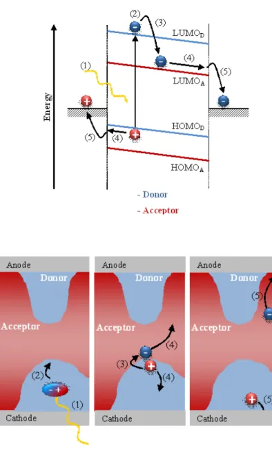
30 and the corresponding acceptor level has to be larger than the exciton binding energy, in order to initiate a charge transfer from donor to acceptor material. If the exciton reaches this donor-acceptor hetero-interface by diffusion, it is energetically favorable for the electron to be transferred to the acceptor molecule. This charge transfer, or electron transfer, is reported to be very fast. Indeed, it was found to be faster than 100 fs in polymer-fullerene systems, and very efficient, as the alternative loss mechanisms are much slower [4]. Thus, the exciton is dissociated and the resulting charge carriers are spatially separated. Even though the electron and the hole now reside on two separate materials, they are still Coulomb bound due to the weak screening of the electric field in organic semiconductors. Therefore, a further step is needed for the final charge pair dissociation, for instance initiated by an electric field or the energetic disorder of the organic semiconductors. Thus, the mutual Coulomb attraction is overcome. This dependence becomes evident in the strongly field and temperature dependent photocurrent of organic solar cells, which also influences fill factor and short circuit current: only if this charge carrier separation is successful, can electron and hole hop towards their respective contacts, in order to generate a photocurrent. The organic bilayer solar cells invented by C. W. Tang were made of two conjugated small molecules, and achieved a power conversion efficiency of about 1 % [2]. The limiting factor in this concept is that for a full absorption of the incident light, a layer thickness of the absorbing material has to be of the order of the absorption length. This is much more than the diffusion length of the excitons [5] so the potential of the bilayer solar cell is difficult to exploit. In the early nineties, a novel concept was introduced, accounting for the low exciton diffusion length in disordered organic semiconductors, as well as the required thickness for a sufficient light absorption: the so-called bulk heterojunction solar cell [6]. This approach features a distributed junction between donor and acceptor material: both components interpenetrate one another, so that the interface between them is not planar any more, but spatially distributed. This concept is implemented by spin coating a polymer-fullerene blend, or by co-evaporation of conjugated small molecules. Bulk heterojunctions have the advantage of being able to dissociate excitons very efficiently over the whole extent of the solar cell, and thus generating electron-hole pairs throughout in the film. The disadvantages are that it is somewhat more difficult to separate these still strongly Coulomb bound charge carrier pairs due to the increased disorder, and that percolation to the contacts is not always given
PhD Thesis in Energy, Eng. A. Calabrese
31 in the disordered material mixtures. Also, it is more likely that trapped charge carriers recombine with mobile ones. However, the positive effects on the device performance exceed the drawbacks. For an efficient bulk heterojunction solar cell, a good control of the morphology is very important. Rather simple methods of optimization have been successfully performed in the last decade. The choice of solvents [7] as well as the annealing of the solution processed polymer-fullerene solar cells [8] both lead to a more favorable inward structure in view of the dissociation of bound electron-hole pairs and the subsequent charge transport. Thus, the power conversion efficiency was increased many fold, in case of the annealing from a bare half percent to above 3 %. Indeed, optimization by novel routes is an ongoing process, and within the last five years, further steps in improving the power conversion efficiency have been made. Co-evaporated copper phthalocyanine/fullerene solar cells have reached 5.0 % efficiency using a concept called planar-mixed heterojunction [9], and solution processed polythiophene-fullerene cells achieved between 6 and 8% efficiency by the use of novel materials as well as additives optimizing the phase separation [10].
2.3 OPERATING PRINCIPLES
Photovoltaic cell configurations based on organic materials differ from those based on inorganic semiconductors due to the fact that the physical properties of inorganic and organic semiconductors are significantly different. Inorganic semiconductors generally have a high dielectric constant and a low exciton binding energy. Hence, the thermal energy at room temperature is sufficient to dissociate the excitons created by absorption of photons into a positive and negative charge carriers. The formed electrons and holes are easily transported as a result of the high mobility of the charge carriers and the internal field of the p-n junction. Organic materials have a lower dielectric constant and the exciton binding energy is larger than for inorganic semiconductors, hence dissociation into free charge carriers does not occur at room temperature. To overcome this problem, organic solar cells commonly utilize two different materials that differ in electron donating and accepting properties. These are called Donor (D) and Acceptor (A) materials respectively.
PhD Thesis in Energy, Eng. A. Calabrese
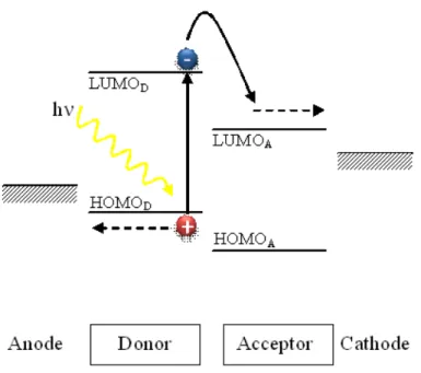
32 Charges are created by photoinduced electron transfer between the two components. This photoinduced electron transfer between donor and acceptor boosts the photogeneration of free charge carriers compared to the individual, pure materials, in which the formation of bound electron-hole pairs, or excitons is generally favored. Various architectures for organic solar cells have been investigated in recent years. The Figure 2.1 illustrates the physic processes involved in transformation of solar energy into electricity in organic photovoltaic device. This scheme, despite its limitations, is generally accepted to explain the mechanism operating in an organic solar cell [11]. In general, for a successful organic photovoltaic cell, five important processes have to be optimized to obtain a high conversion efficiency of solar energy into electrical energy.
1. Photons absorption and generation of excitons: light causes the promotion of electrons from the highest occupied molecular orbital (HOMO), analogous to valence band in the inorganic semiconductors, to the lowest unoccupied molecular orbital (LUMO), analogous to the conduction band in the inorganic semiconductors, of the donor material. The processes can also occur in an analogous manner in the case of an excited acceptor, and the details of these mechanistic steps have been described extensively in the literature but is not object of this work. This results in an excited but neutral state with a limited, finite lifetime; this state is termed exciton and consists of an electron and a hole paired by an energy Eex that is smaller than the energy gap between the limits of the permitted
bands (difference between LUMO and HOMO orbital of donor material). If Eg is
the energy gap, then (Eg− Eex) is the exciton binding energy (around 0.4 - 0.5 eV in
conjugated polymer [1]) indicated with EB. The amount of absorbed photons
depends on the value of the optical absorption coefficient and on the thickness of the donor material.
2. Excitons diffusion: these quasi-particles diffuse within the material as long as recombination processes (of the hole-electron pair that forms/constitutes the excitons) do not take place.
3. Hole-electron separation (excitons dissociation): if the offsets of the energy levels of the Donor and the Acceptor materials are higher than the exciton binding energy, excitons dissociate at the D/A interface. More precisely, the condition that must be fulfilled is Eex > IP − χ, where Eex is the exciton energy, IP is the ionization energy
PhD Thesis in Energy, Eng. A. Calabrese
33 of the acceptor, and χ is the electronic affinity of the acceptor [12]. Excitons photogenerated in the donor side will dissociate by transferring the electron to the LUMO level of the acceptor and retaining the positive charge, while those created in the other phase/component will transfer the hole to the HOMO of the donor while retaining the negative charge. This step leads to the formation of free charge carriers.
4. Carrier transport towards the electrodes: this transport involves the classic
mechanism for hopping processes in organic materials.
5. Charge collection at the respective electrodes: for this to occur most efficiently, the following conditions (opposite to the injection conditions for OLEDs) must be met:
EF cathode < ELUMO acceptor and EF anode > EHOMO donor.
Each of the above listed steps can be affected by several phenomena that decrease the efficiency of the global process, so that only a limited portion of the photons reaching the cell are able to generate useful charge carriers. Thus, the optimization of each step is extremely important to extract as much energy as possible from the device. This optimization encompasses the development of improved approaches in the design of materials and device structures.
PhD Thesis in Energy, Eng. A. Calabrese
34
2.4 DEVICE PHYSICS
In this section, the function of an organic solar cell will be described in more detail as compared to the preview introduction, including loss mechanisms and other limitations. The section is ordered according to the different steps from photon absorption to photocurrent generation, as described above for a bulk heterojunction solar cell.
2.4.1 PHOTON ABSORPTION AND EXCITON GENERATION
A basic requirement in an organic photovoltaic cell is that the materials optical excitation energy gap (optical gap) should be equal or close to the incident photon energy. In most amorphous organic materials where electronic band structures are difficult to form, this gap is the energy gap between the Highest Occupied Molecular Orbital (HOMO) and the Lowest Unoccupied Molecular Orbital (LUMO), both are also called frontier orbitals. In organic conjugated system, HOMO is typically an occupied π bonding orbital, and LUMO is typically an unoccupied π* anti-bonding orbital. Since an organic HOMO/LUMO excitation basically generates a tightly bound exciton instead of a free electron and hole, optical energy gap is therefore used instead of the conventional electronic energy gap that typically refers to the energy gap between the free holes at valence band (VB) and the free electrons at conduction band (CB) in inorganic semiconducting materials. In organics, the relationship between optical gap (Egopt) and electronic gap (Ege) may be approximated as:
e opt B
Eg Eg E (1)
where EB is called exciton binding energy that represents a minimum energy needed to
separate an intra-molecular exciton into an inter-molecular radical ion pair [13]. Egopt
values can be estimated directly from optical absorption band edge, and absolute Ege
values may be estimated by electrochemical Redox analysis. Absolute HOMO/LUMO levels are typically estimated from a referenced half electrochemical analysis in
PhD Thesis in Energy, Eng. A. Calabrese
35 combination with the optical absorption spectroscopy. Solar light radiation span a wide range with largest photo-flux between 600–1000nm (1.3–2.0 eV, on surface of the earth or 1.5 Air Mass) or 400–700 nm (1.8–3.0 eV, in space or Air Mass 0). So, for terrestrial applications, it is desirable that the energy gap of the donor material span a range from 1.3 to 2.0 eV. This may be achieved by incorporating a series of different energy gaped donor/acceptor or organic dyes that absorb light in that radiation range. However, while the solar photon loss can be minimized in this way, due to energy transfer processes where all high energy excitons will eventually become lowest energy excitons, the open circuit voltage (Voc) of the cell will also be reduced accordingly. Indeed, experimental studies have revealed certain correlations of Voc versus the gap of lowest acceptor LUMO and highest donor HOMO levels [14]. Actually, several widely used conjugated semiconducting polymers used in organic solar cell studies have optical gaps higher than 2.0 eV, well above the maximum solar photon flux range. This photon loss problem is in fact very common in almost all currently reported organic photovoltaic materials and devices. However, one advantage of organic materials is the versatility and flexibility of its energy levels being fine tuned via molecular design and synthesis, therefore, ample room exists for improvement.
2.4.2 EXCITON DIFFUSION
Once an organic exciton is photogenerated, it typically diffuses (e.g., via intra-chain or inter-chain energy transfer processes) to a remote site, and at the same time it quickly decays radiatively or non-radiatively to its ground state, having usually pico to nano seconds lifetime. Alternatively, in solid state, some excitons may be trapped in certain defect or impurity sites. Both exciton decay and trap contribute to the exciton loss. For most conjugated organic materials the average distance an organic exciton can travel within its lifetime is typically in the range of 5-10 nm [5, 15]. Since the desired first step of photovoltaic process is that each photogenerated exciton will be able to reach the donor/acceptor interface where charge separation can occur, one way to minimize the exciton loss would be to make a defect-free, a donor/acceptor phase separated and ordered
PhD Thesis in Energy, Eng. A. Calabrese
36 material. This could be obtained by a bulk hetero-junction structure. This type of solar cells are desirable, as they not only minimize the exciton loss by increasing the donor/acceptor interface, they can also offer enough thickness for effective photon harvesting.
2.4.3 EXCITON SEPARATION AND CHARGE CARRIER GENERATION
As discussed, the exciton binding energy is much larger than the thermal energy in organic semiconductors. Thus, in view of photovoltaic current generation, a driving force is needed to dissociate them. As already outlined in the previous section, its lack is the reason why single layer organic solar cells doesn’t work efficiently. A second organic semiconductor, the electronegative acceptor, has to be introduced either in a bilayer or bulk heterojunction device configuration in order to yield an efficient exciton dissociation. The class of materials with the currently best acceptor properties are the (buckminster)fullerenes, C60
and its derivatives. Polymer acceptors and non-fullerene small molecule acceptors have shown a less efficient excitons separation of charges up to now, which seems to be due to the LUMO not being electronegative enough for efficient electron accepting properties and too low electron mobilities [16].