Chapter 1
S
ENSOR
S
YSTEMS IN
I
NDUSTRIAL
A
PPLICATIONS
1.1 Sensor market overview
In the last few years the density of electronic devices has exponentially grown thanks to the recent technological advances. Moreover the new progresses of micro-mechanical technology have featured the miniaturisation of sensing elements achieving complete sensor systems on a common substrate of silicon with the conditioning electronics. The new potentialities of MEMS devices have opened the way for a broad diffusion of sensing and actuating systems in a wide range of application fields. In fact, if in the last decades the diffusion of sensors and complete measurement systems was limited by the costs, the size and the low reliability, the new generations of MEMS sensors achieve high reduction of costs, area and power consumption. These systems have proven to be a key enabling technology of developments in areas such as transportation, telecommunications and health care, but the range of MEMS applications covers nearly every sector. According to latest updated technical market research report (a comprehensive new market research from SEMI and Yole [1] July 18, 2007), the global market for MEMS devices and production equipment reached $40 billion in 2006, and is expected to rise to $56 billion by 2009 and $72 billion by 2011, for a compound annual growth rate (CAGR) of about 12% over the five-year.
The MEMS devices at the heart of these systems overall amounted to $5.9 billion in 2006, and are forecast to grow to $10.8 billion in
2011, with a compound annual growth rate (CAGR) of 13 percent (refer to Figure 1-1), pushed by the emerging employment in consumer electronics. MEMS devices are defined as die-level components of first-level packaging, and comprise pressure sensors, micro-resonators devices, accelerometers, gyroscopes, micro-RF devices, microphones, digital mirror displays, anemometers, etc.
Figure 1-1: Global MEMS market 2005 2010 [2].
MEMS materials market can be partitioned into substrates and chemicals and other materials: together these markets consisted in $433 million in 2006 and are forecast to reach $806 in 2011. All materials are expected to be subject for five-year to a CAGR of 13% up to 2011 pushed by a demand driven by substrates, (representing more than 70% of the market), packaging coatings and emerging employment of chemical mechanical planarization (CMP). The MEMS equipment worldwide market amounted to $646 million in 2006, and is forecasted to achieve $838 million in 2009 and $999 million in 2011 with a five-year CAGR forecast for of 9%. Demand for MEMS equipment and materials also is poised for solid growth thanks to the increasing employment of etching technologies (notably deep reactive ion etch) by MEMS
Markets 2006 2011
Compound Annual Growth Rate
MEMS
Materials $433 million $806 million 13% MEMS
Equipment $646 million $999 million 9% MEMS
Devices $5.9 billion $10.8 billion 13% MEMS
Systems $40 billion $72 billion 12%
Table 1: Global Markets and Forecasts for MEMS Systems, Devices, Materials and Equipment (Yole Development) [2]. The world MEMS sensors market is fuelled by the increasing demand from different application fields, such as automotive and consumer electronics. The outstanding success of electronic stability control (ESC) and electronic safety active assistance systems joined with regulations passed by the worldwide safety authority that impose a growing adoption of security control in automobiles, are pushing the growth of the automotive segment. Furthermore the automotive technology has opened the way for the adoption of inertial sensors for adding functionality and safety in devices such as mobile phones, gaming devices and notebooks, determining a vertical growth in the consumer segment.
MEMS-based systems are also estimated to have a considerable potential in market segments such as life sciences, defence and environmental monitoring and protection, leading to continued commitment by government authorities and governmental agencies for this technology. The US and the European Union are promoting increasing investments in the employment of MEMS technology for a wide range of applications.
Furthermore funding from venture capitalists (VCs) is also expected to play a key role in the growth of the world MEMS sensors market.
Although the MEMS market is currently fragmented, both in terms of the types of devices being produced and the companies producing them (see Figure 1-2) the latest projection [2] states that in the upcoming future over the next ten years, MEMS components trend will follow an increasing integration into single modules that will replace existing electronics systems. Moreover MEMS manufacturing will be absorbed by mainstream semiconductor companies. Nowadays it is a matter of fact that MEMS technology is replacing a growing number of non-silicon devices and the global sensor market is migrating from the
component sensors to integrated devices. For example, several leading companies, (including Bosch, BEI Technologies, Invensense, and Honeywell) are focusing on MEMS-based inertial measurement systems to substitute non-silicon accelerometers and gyroscopes not only for automotive applications but also for a wide range of other fields, and even companies such as Knowles and Akustica are merging silicon microphones into acoustic devices. Furthermore, companies oriented to consumer applications are pushing the demand for integrating MEMS devices into modules aimed at replacing optical auto-focus and zoom functions in mobile phones [3].
Figure 1-2: Global MEMS market 2006 (source WtC) [5]. As a result of this trend a high level of interest has arisen around MEMS technology from twofold directions: business and technical directions. On business side MEMS systems are proved to be increasingly attractive because multiple emerging markets for MEMS devices promise large financial gain and this potential for growth is confirmed by a growing amount of venture capital industry investment into MEMS based companies [2].
On the other hand technical attractiveness is determined by multiple factors:
• The cost of the single sensor device is directly related to its size and, as it does for ICs, it scales down with the upcoming
devices thanks to the removal of mechanical fatigue and hysteresis phenomena. In single crystal form, silicon is an almost perfect Hookean [1] material, thus when it is flexed there is virtually no hysteresis and hence no consequent energy dissipation. Moreover silicon perfectly fits applications in which repeatable motions are required since it suffers very little fatigue thus featuring lifetimes in the range of billions to trillions of cycles without breaking. Its mechanical properties are comparable to steel (see Table 2).
Steel Silicon Units
Yield strength < 4.2 7.0 10 10 dyne/cm2 Young`s Modulus 2.1 1.9 10 12 dyne/cm2 Density 7.9 2.3 Gram/cm3 Thermal conductivity 0.97 1.57 W/cm°C Mechanical hysteresis Yes No Sensitivity to
stress Low High
Fabrication
resolution 10 0.01 µm
Fatigue failures Yes No
Table 2:Mechanical properties of steel versus silicon [1]. • Technology infrastructures for developing MEMS are already
available and quite well established, comprising: batch-wafer processing, cutting-edge IC processing equipment, complicated diagnostic equipment, design and simulation tools, and high-volume IC packaging technologies, even though new technology progresses always require a continuous research for new development and design strategies for facing the growing market demand.
• System on a chip can be created embedding conditioning electronic on the same silicon substrate (system on a chip) or at least on the same package (system on package) for developing low-cost integrated mechanical, optical, and biological systems.
• The pool of educated silicon processing technologists is available even though the market demand requires always new forces.
• MEMS can be used as a packaging vehicle for nano devices, suggesting synergy with nanotechnology.
Furthermore there is now a widely shared vision among chip designers, suppliers, as well as original equipment manufacturers (OEMs) and this promises a clear commitment for improvising the use of the technology in a wide range of market segments. In addition the growing popularity of novel features related to sensing introduction in the final user’s applications is expected to spur the use of sensor system in particular fields such as consumer, automotive (e.g. the increasing demand for advanced safety systems as well as driver infotainment systems on chips in automobiles, see Figure 1-3).
Figure 1-3: Sensor Systems in Automotive (source WtC)[4].
1.2 MEMS applications
Microelectromechanical systems represent the outstanding state of art for a broad range of mechanical, chemical, optical, and biotech products (sensors, microstructures and actuators) fabricated as integrated circuits on silicon wafers in a batch mode. Commercial MEMS products comprise flow sensors, pressure sensors, acceleration sensors, gyros, ink-jet nozzles, head locators in hard drives, and digital light processors (DLPs) in projectors and screen sets.
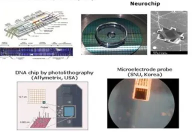
i. Life science applications
A huge number of applications are adopting MEMS inertial sensors, since MEMS-system-based inertial and motion sensors employment in medicine applications is fuelled by the demand for implantable devices that must be highly reliable and very small, as well as by handheld devices for patient monitoring and diagnostics at home (see Figure 1-4). In 2006, medical applications accounted for 12.7 percent of total MEMS revenues; in 2011; they're forecast to account for 11.3 percent of revenues of the total MEMS market [7]. MEMS offer a particular advantage to the medical field; in fact Bio-MEMS leverage chemical functions, mechanical functions, electrical and neural functions of microstructures in ways that mimic or interact with the way that the human body adopts. Some of the specific advantages of BioMEMS are:
• Biocompatibility, since silicon is biocompatible • Greater uniformity and reliability
• Reproducibility
• Miniaturized implants
• Ability to respond on short time scales • Ability to provide electrical stimulus • Low power applications
• Both optical and electrical sensitivity
• Possibility to integrate conditioning electronic and sensor on the same chip
• Capability to interact with fluids and micro-fluidics.
• Precise control, quick response, short time scale operation, response to electrical stimulus (e.g. for drug delivery applications).
• Miniaturization and ability to measure physiological signals as well as the ability to provide electrical impulses, (e.g. for pace maker applications).
Bio-MEMS also feature non invasive/painful procedures and information retrieval (e.g. pressure sensors can be used in cardiovascular monitoring, glaucoma monitoring, and monitoring of intracranial pressure). Moreover MEMS technology is also pushing the development of medical centres of new conceptions with smart surgical instruments that allow the risk and length of surgery to be lowered, decreasing patient recovery time and reducing the overall costs of healthcare delivery [8].
There is a great interest in trying to monitor the activity of people who are at medical risk or who, for simply aging, can find themselves in a situation in which they require immediate assistance. Motion sensors can go in this direction preventing
people from falling or alarming when a plunge is happened, for example STMicroelectronics introduced ultra-compact low-g linear accelerometers in 2007 for use in health monitoring, featuring compact size and low power consuming system with a monitoring unit for remote data transmission (ST's LIS244AL incorporates a dual-axis MEMS sensor and a CMOS interface chip in a single package offering a full-scale output range of ±2.0 g and provides shock survivability).
Another important segment for medical applications of MEMS is the so called Lab-On-a-Chip (LOC) which indicates a term for devices that integrate (multiple) laboratory functions on a single device of reduced size and that are capable of managing extremely small fluid volumes down to less than pico-liters. The main advantages of LOC can be found in their capability for performing a series of delicate analysis in short time and with a constant and low cost monitoring of the patient under examination. Examples of LOC application are in real-time PCR (detect bacteria, viruses and cancers), immunoassay (detect bacteria, viruses and cancers based on antigen-antibody reactions) dielectrophoresis (detecting cancer cells and bacteria), blood sample preparation (can crack cells to extract DNA), cellular lab-on-a-chip for single-cell analysis.
Figure 1-4: An example of MEMS Systems in Bio-medical applications.
ii. Communications: RF MEMS
Microelectromechanical Systems applications in RF and microwave electronics are revolutionizing wireless communications. In particular, RF MEMS promises to provide wireless handsets, base stations and satellites with the key properties of low-power consumption, low area occupation and enhanced re-configurability, which can result in superior functionality and performance. For these potentialities and since they are expected to substitute existing products and enable new applications (especially mobile phones) MEMS market is estimated to reach $390 million in the wireless handset applications in 2011 [2]. Extensive researches have been conducted in the area of wireless front-end circuitry aiming at the implementation of efficient, CMOS-compatible, components such as inductors, tuneable filters, however, these components typically suffers by high loss which translates into poor noise characteristics or low Q factors and represent a major design bottleneck, on the other hand RF devices based on MEMS all feature low loss, high Q factor, high linearity and good power handling [10]. There are various types of RF MEMS such as capacitors, inductors, resonators, varactors (variable capacitors in which the capacitance is controlled by varying the gap between two plates, typically by means of electrostatic force) and switches. RF MEMS switches can be classified by actuation method (electrostatic, magnetic, piezoelectric, thermal), by contact mechanism (capacitive, metal-to-metal), or by anchor mechanism (cantilever, fixed-fixed beam) [9]. Typical MEMS switch types are composed by a thin metal cantilever, a bridge, a diaphragm (or some similar structure) to open an RF transmission line or shunt it to ground. MEMS switches feature excellent RF characteristics, including insertion loss values of approximately 0.1 dB and isolation values of approximately –30 dB in series-configured switches at lower RF frequencies (VHF to ~10 GHz) and in shunt-configured switches at higher frequencies (~10 to 100 GHz). Such devices outperform many traditional RF circuits, such as switchable routing in RF system front-ends, and routing in time-delay phase-shifter networks. Furthermore thanks to the employment of RF MEMS the RF market will face new class of electrically reconfigurable antenna system, even though the replacing of traditional structures by MEMS ones is still critical in cell phones, because of switching speed limitation [2].
Figure 1-5: An example of MEMS electrostatic actuated switch.
iii. Automotive
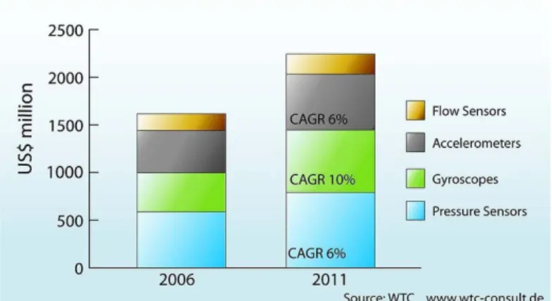
MEMS devices got their start in the automotive industry: starting from the 1960s, the motor vehicle industry has gradually introduced electronic technology to perform many of the control functions previously performed mechanically or by hydraulic actuators and today's high-end vehicles feature up to 100 different sensors among which about 30 these are now MEMS, and the percentage is forecasted to grow. The market is composed by accelerometers, gyroscopes, pressure and flow sensors. Latest applications comprise IR sensors for air quality, micro-mirrors for displays. According to [1] the automotive segment is accounted for $1.6 billion, making this the second biggest opportunity after IT peripherals and inkjet print heads. By 2011 the market will top $2.2 billion, with a CAGR of roughly 7% (see Figure 1-6).
Figure 1-6: Market for Automotive MEMS sensor (source wtc-consult).
Hereafter we depict some of the main sensing applications in the automotive sector:
• Active safety represents the most important requirement in
modern vehicles. The MEMS accelerometers and gyroscopes are both sensors which can perfectly fit active safety requirements in the automotive domain [11]. The well known
ABS (Anti-lock Braking System) prevents the wheels from
locking while braking, Cornering Brake Control (CBC) performs stabilisation during partial braking whilst cornering. Traction
control system (TCS) is designed to prevent loss of traction.
Furthermore sensor systems are employed in the correction of drive trajectory: Electronic (Dynamic) Stability Control (ESC, ESP) compares the driver's intended direction, to the vehicle's response, via lateral acceleration, rotation (yaw) and individual wheel speeds. ESC then brakes individual front or rear wheels and/or reduces engine power as needed to get correct under steer or over steer. Some systems feature anti collision detection like Adaptive (Active, Intelligent) Cruise Control (ACC, ICC) which uses either a radar or laser setup to slow the vehicle when approaching another vehicle and Lane Departure
Warning system (LDW) which warns the driver when the
vehicle begins to move out of its lane.
• Intelligent Light Positioning is gaining relevance in high end
cars and is expanding down to more market segments. MEMS sensors like accelerometer and gyroscope can lead to a new generation of head lights enhancing road illumination and guaranteeing safer driving conditions. Thanks to motion detection, and assisted by GPS systems alignment of head light to various road conditions (e.g. asphalt, curves, uphill,
downhill) and on vehicle condition (e.g. speed type pressure, suspensions, number of occupants).can be automatically performed.
• Intelligent Air Bags care to soften impact for passengers during
car crashes. Since the airbag system must act at the right instance and also with the proper force toward the car occupants, the identification of type of collision, its direction, g-force impact assume critical importance. The adoption of MEMS accelerometer, thanks to their high integration capability and accuracy, can lead to detection system of new generation replacing standard electromechanical system, achieving enhanced passenger care. Since the instant of the impact cannot be predicted in advance, it is extremely important to detect for each passenger the seat position and if in the crash the occupant is lifted from the seat. The MEMS accelerometer can determine the correct positioning of car occupants to dose the force of airbags bang.
• Vehicle Monitoring is devoted to check up the car condition to
anticipate the detection of any malfunctioning. The tire correct condition can be determined through tire pressure sensors, and MEMS sensors, thanks to the compact size and high accuracy, embody optimal candidates. Furthermore the monitoring of machine vibrations can avoid excessive power consumption and accelerated wearing on bearings, seals and foundations. Vibrations can be detected by accelerometer systems for measuring vibrations frequency, amplitude (strength) and spectrum (signature) to identify the particular vibration.
• Satellite navigation systems in vehicles can determine the
position of the car anywhere on the world by radio signals from Global Positioning System (GPS) satellites. Nevertheless, data from satellite is not sufficient to constantly determine the correct positioning since the satellite signal could not be always available due to shadowing by buildings and overpasses especially in crowded urban areas. In this scenario, a dead reckoning GPS system can replace the navigation system continuing tracking movements during the time when satellite signals are not available. MEMS-based gyroscope and a magnetometer can path the motion direction and together with an accelerometer can implement complementary tracking system to GPS.
can notice the change in inclination and activate the alarm and security system.
iv. Commercial applications
Since last few years MEMS devices have approached the commercial market taking advantage of the depth and breadth of what this technology has to offer. MEMS application are well established in specialized markets, primarily automotive, industrial and medical, and the conditions are mature for impacting the consumer market not only regarding the inkjet printers but for a wide spectrum of applications. The acceleration of MEMS diffusion in consumer product categories in these years and beyond will involve both continuous growth in existing markets as well as huge growth in new applications for any device that might offer a better man-machine interface [12].
Hereafter we resume the main field of applications for consumer market:
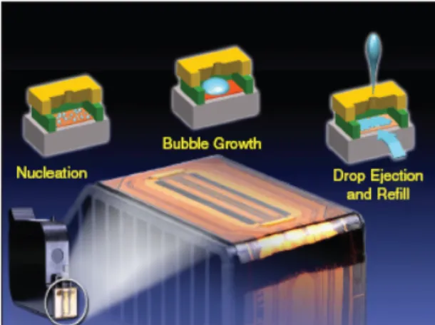
• Ink-jet print heads can be implemented effectively with MEMS
technology: they feature hundreds of microscopic channels connected to ink-filled chambers and thanks to silicon’s thermal conductivity, each chamber can be heated very rapidly by a resistive heating element, vaporizing part of the ink and propelling the volume of ink towards the paper in a tiny droplet (see Figure 1-7). In this device, the only moving ‘part’ is the ink. The micro-machined device is assembled on the edge of the ink cartridge [6].
Figure 1-7:An example of Inkjet cartridges (courtesy of STMicroelectrinics).
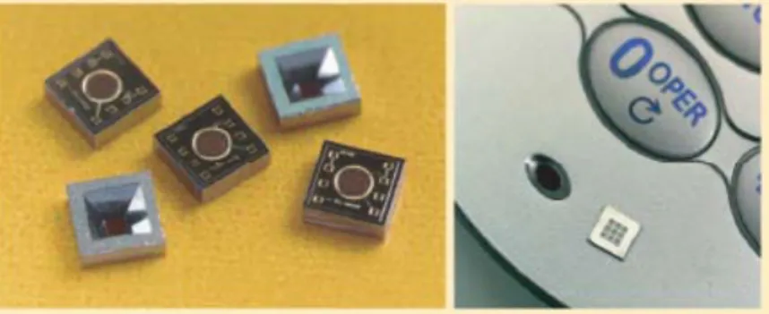
• Silicon microphones are gaining a huge importance thanks to
the high performances obtained in low size. Typically pressure sensors devices are made of two chips in a single package: the sensing element which is a micro-machined capacitor able to detect changes in atmospheric pressure caused by sound signals and the electronic conditioning chip which amplifies the small signal and provides the output data (see Figure 1-8).
Figure 1-8: An example of MEMS Microphone (courtesy of Knowels and Acustika).
• Hard Disk Drive (HDD) Free Fall protection. In HDD-based
devices like MP3 and MP4 players, laptops and mobile phones, the use of three-axis accelerometers can prevent the HDD from any potential loss of stored data caused by accidental fall. Actually, if the a device falls, the accelerometer senses the zero-gravity, and the dedicated electronic sensor interface provide to keep the read/write head apart from the sensitive disks before the head can crash onto the disk itself, causing possibly damaging the drive.
• Gaming Interfaces are very attractive for involving the user in
the game itself for providing the gamers “real” sensations gaming in portable devices. Thus, adopting accelerometers an easy-to-use interface can be obtained by sensing hand/fingers/wrist motion and translating that motion to an action in the game. Therefore the single-handed operations and gesture recognition can be added to gaming devices. As example a more recent and highly publicized application of motion sensing MEMS components is in the latest gaming consol of Nintendo Wii which features a wireless motion control application based on accelerometers: the motion detection of a player’s hand in three dimensions and response to changes in
• Digital Still camera image stabilization is becoming a must for
all camera makers and not only in high class camera segment. Piezoelectric vibrating gyroscopes are used for image stabilization: they offer the advantages of reduced dimensions and lower power consumption; furthermore, they can measure angular rate along pitch and roll axes simultaneously and can be integrated more easily with other motion sensors. In addiction not only classical camera devices take advantage of MEMS stabilization, the increasing number of mobile phones with cameras represents a market opportunity of several hundred million devices per year.
The consumer market is looking for tiny, low cost, low-power consumption devices. Mobile phones, MP3 and MP4 players, and digital cameras, gaming consoles, portable PCs are all battery-operated and are becoming smaller and thinner. Furthermore, the product life cycle of consumer devices is shorter than the one in automotive markets; therefore, making MEMS system suppliers to face an increasing reduction in time to market for developing new products.
v. Industrial applications
MEMS sensors are finding their way into an increasing number of industrial applications, including workplace safety systems, process control, equipment position, impact detection and environmental monitoring.
Recent requirements for safety in work places has lead the adoptions of accurate means for providing detection of potentially dangerous operating conditions without impacting normal operation. One of the primary factors in this process is the accuracy of the sensing solution used to detect the dangerous operating conditions. MEMS accelerometers respond to the demand for accurate monitoring system which can be diffusively disposed in industry implants for diffusive supervision.
Another industrial segment which is significantly growing in the last few years regards the micro-drives: typical micromechatronic systems that can generate motion. They typically consist of elements capable of processing information and energy and can be employed for fine refinements and advanced operations in which extreme accuracy is required. The core element of any micro-drive is the energy converter (micro actuator), which converts energy into mechanical motion energy. As example in micro-mechanic switches standard relays are going to be replaced though solutions using MEMS devices empowered by driving electronics.
Process control is a key application in industrial segment for dosing reagents in chemical reaction control. MEMS devices play a key role in providing instruments for synthesizing and analyzing (bio)chemical materials of higher quality, at higher throughputs and against reduced costs. Furthermore a fundamental factor for achieving the successful breakthrough of micro-reactor technology in fine chemistry and industrial process control consist in the ability to combine single components in efficiently working systems of a larger complexity. The chemical analyses are performed by different types of chemical sensors, for example spectrometers (detecting the chemical composition of a substance by measuring its absorption or emission spectra). One revolutionary nanotechnology development is represented by cylindrical carbon molecules (CNTs) with properties that make them potentially useful in extremely small-scale electronic and mechanical applications [13] [14]. They exhibit good strength and unique electrical properties and are efficient conductors of heat. In addiction with MEMS devices the optimization of process parameters and production of the complete annual production volumes can be performed in the very same system, bypassing the expensive and time consuming stage of up-scaling production processes answering quickly market demands.
Furthermore MEMS devices can be effectively employed for industrial robots, as the technology can apply to tactile sensors, navigation, or proximity sensors. In fact MEMS technology features lower-cost tactile sensors, which can enable a robot to obtain sensing information in order to make decisions and to execute actions in a more accurate and autonomous manner. As example, robotic sensing activity makes extensive use of inclinometers, a specialized version of accelerometers, which indicate deviation from the vertical by sensing the downward G force. Thus the inclinometers gain an accurate reading for the position and motion of a robotic arm and makes it possible to control the arm more precisely, while speeding up its operation.
Industrial and environmental monitoring [15] can take advantage of the MEMS technology with a twofold benefit: the sensing system can be directly posed in contact with the media to monitor thanks to the reduced size and the possibility to make the sensor cooperate with electronics; and in merit to the cost reduction brought by the MEMS sensing equipment the monitoring can be extended not only in critical points but can be disposed diffusively for a complete coverage of the system (e.g. diffuse monitoring of
vi. Military and Aero-space application
At the very first, MEMS sensors have started to be employed in the military and aerospace applications, and immediately after exported to the automotive segment. The first silicon pressure sensors were introduced to the market in the 1960s for military and aerospace purpose. Acceleration MEMS-based sensors were developed for the military and aerospace markets in the 1970s. MEMS rate/gyro sensors were developed in the 1990s, first for military, then automotive applications.
MEMS technology has enabled smaller, low power, and low cost micro-instruments currently including pressure, flow rate, acceleration, angular velocity, and MEMS actuators such as valves, synthetic jets, boundary layer trip devices, micro jet engines and microthrusters that have supported a variety of aerospace missions [16]. Hereafter we depict a series of the major aerospace and military applications:
• Microsetellites can benefit by MEMS devices since it is possible to establish much lighter and smaller satellites with higher performance and longer lifecycle. The power cost of MEMS device is usually much lower than traditional devices, which will greatly reduce the consumption of power. Furthermore for its small size and low power consumption MEMS devices are particularly fitting the request for redundancy which is a must for space applications. For example launched on 18 April, 2004, HS-I is a nano-satellite for science exploration and MEMS devices test. It consists of several MEMS devices, including micro CMOS cameras, sun sensor, momentum wheels, and micro magnetic sensors [17].
Figure 1-9: a) launch from a mother ship of b) microswitch in MEMS technology.
• Micro-propulsion systems. Micro-thruster can be developed
surface cavities become tubes and large cavities become propellant tanks. MEMS valves, pumps, mixers, flow monitors, and temperature sensors have already been studied [18][19][20][21][22][23] and all these device can be combined for developing a complete system for micro-propulsion. As a complete system, MEMS thruster development is less mature, but significant research efforts have been initiated [24] [25]. A very ambitious and employment of micromachined actuators for both propulsion and energy conversion is illustrated which present a jet engine with a complete gas turbine on a chip [26].
• Navigation assistance is fundamental to help the pilot in
guiding complex machines (e.g. tanks, jets) and empower his capability. MEMS accelerometers, gyroscope can fit this demand and provide accurate and low power devices for guidance assistance and also for complete autonomous system drive like rockets and satellites.
• Equipment monitoring of the complex structures adopted in
military and aerospace segment is mandatory. A continuous check of the functionality of the global structure has to be continuously implemented to guarantee the effectiveness of the target device and assure safety issue for the users of the machine (from a single life jacket to a tank) For example MEMS pressure sensor have been tested in the booster rocket of the ejection seat used in the F-14 fighter. Furthermore the monitoring of military devices often exposes sensors to harsh environments (e.g. monitoring the dynamic internal behavior of prototype jet turbine engines) MEMS sensor can respond to these thigh requirements.
1.3 Specifications for sensor conditioning
electronics
The design of electronics for the wide range of application fields have to necessarily conform to the severe specifications of the relevant market segment. A strict requirement imposed by market demand concerns performances, expressed in terms of power consumption, area and cost. The control for power consumption represents indeed a key issue for mobile and stand-alone applications especially when MEMS device are employed in fields
pushing towards a reduction of available power for each electronic system, together with the need to combine multiple functionalities inside a smaller number of modules in order to optimize power consumption and also to lower the cost related to these electronic systems.
A delicate subject for sensor system designers concerns the reliability issues. This aspect assumes low relevance with consumer devices but it gains extreme importance in automotive market and is of unquestionably importance in military applications and in critical industrial control in which human life can be injured. Robustness is a powerful mean to attract customers and claim superior quality with respect to competitors for cars manufacturer and is a must when the sensor system has to be delivered for military purpose. For this reason product factories tend to raise as much as possible the expectations on the operative life of the overall product, resulting in always tighter specifications for the related electronics. Electronics, as a part of a final product, has to guarantee the compliance to the relevant standards, with the additional complexity of operating in harsh environment. The electronics products are often required to work under extremely hard conditions, for example petroleum vapours, vibration (up to 10g rms near the engine in automotive applications), electro-magnetic interference in RF devices, in a moisture of chemical reagents in process control and subject to sudden acceleration in aero-space applications. It is possible to distinguish different temperature ranges among the main market segments which dramatically affect the design of the overall sensor system, the temperature ranges are summarized in Table 3.
Electronics Operating Temperature
Consumer 0 °C to +70 °C
Industry -40 °C to +85 °C
Automotive -40 °C to +125 °C
Military -55 °C to +125 °C
Table 3: Thermal operating environments [27].
Lengthen exposure to high temperature can definitely badly affect the behaviour of an integrated circuit. The core consequence of high operating temperature is a quicker ageing of the device [28]. In fact, during industrial tests the average life expectancy of a component is statistically calculated from the faults arisen in a lot of test devices working constantly at elevated temperature or subject to a subsequent properly shaped temperature cycles. Experimental laws [29] [30] describe how the junction temperature cuts down the device life time exponentially.
Therefore, as a direct consequence, when a particular sensor system is designed for working at extreme temperatures it becomes critical to perform a precise evaluation of the life expectation of the electronic system.
1.4 MEMS sensing and actuation technology
Micro-machined sensors are designed to detect changes in pressure, temperature, acceleration (or inertia), and other physical entities, while actuators are used to operate physical action (e.g. printing ink on paper, reflecting laser beam in displays, or inoculating medicine in humans).Major MEMS sensing technologies include:
• Piezoresistive and Piezoelectric effect in silicon are based on
changes of electrical quantities caused by mechanical actions and vice versa. In piezoelectric effect sensors are based on deposited piezoelectric layers and respond to a strain change under the application of the input variable. In piezoresistive effect silicon devices under applied stress feature a resistance change that amounts to roughly two orders of magnitude larger compared to changes that would results from dimension change (typical for metals). Thus silicon results as a key material in sensing mechanical movements compared to classical approaches, for example if a metal material is elongated 0.1%, (e.g. typical metallic resistors used for strain gages) the resulting change would amount to 0.2%, but resistance of silicon would vary by about 10% (depending on doping level). Thanks to this physical property that make silicon devices perfectly fit high accurate measurement system, piezoresistive sensors are leaders in the market for pressure, acceleration, and force applications.
• Capacitive sensors are based on capacitance variation
detection caused by a physical force typically pressure, acceleration, or rate. The variation in capacitance value is typically determined by at least one moving electrode under the input variable. The classical structural configuration comprises two flat electrode capacitors, implemented by interdigitated silicon fingers of even staggered capacitors for sensing variation orthogonal to the plane formed by the capacitor plates itself: these structures are widely diffused in
• Resonant sensors are based on resonating beams or
diaphragms. Applied strain changes resonant frequency, enabling measurement of target physical quantities (e.g. pressure, acceleration, rate). Resonant frequencies can be measured in various architectures and sensing technologies [31].
• Thermoelectric sensors are based on a large number of tiny
thermocouples connected in series capable of displaying a voltage difference related to a flow of charge carriers originated by a heat flow caused by a temperature gradient in the conducting material.
Micro-mechanical actuators feature energy conversion from a physical domain to another (e.g. voltage to deflection). The main actuators principles for MEMS devices rely on: electrostatic, magnetic, piezoelectric, thermal, and optical effects.
The electrostatic actuators are characterized by reduced drive energy thus assuming a key role in MEMS actuation applications. A typical drive requires low current with relatively high voltage (up to 500V) which is now dramatically decreasing in the range of 20-50V thanks to the new advances in technology for MEMS fabrication and the adoption of void packaging for reducing significantly the inertial forces.
The electrostatic actuators feature two main implementations: parallel plate and comb drive:
• Parallel-plate actuators are mainly based on an electrode
(typically metal) and the conductive actuator thus featuring a real simple implementation. Parallel plate capacitors are widely employed in a different range of applications: microgrippers, microrelays, micromotors, cantilevers, optical shutters, and in the latest projection displays based on micromirrors.
• Comb drives actuators are designed to reduce drive voltage,
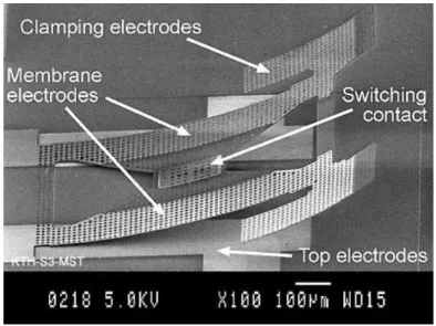
improve drive linearity to voltage, and remove the punch down effect in plate actuators (which physically limits the excursion of the capacitance plates). The gap between comb fingers does not change, as it does in the parallel plate capacitors, since the movements is developed in the parallel direction regards to the plate plane. The actuated force is directly a function of the shaped geometry and the driving voltage, but does not depend by the position of the combs, thus simplifying the electronic control of the actuator. A first implementation of comb drive structure is described in [32], as lateral comb drives (see Figure 1-10). Furthermore comb
drives can also be manufactured in bulk silicon by deep reactive ion etching. A variation on the comb drive design is a vertically asymmetric comb; the differences in height and lateral restriction determine a vertical movement of the comb structure instead of lateral shifting. This approach features larger deflection with low applied driving voltages but results in a more difficult technology implementation.
Figure 1-10: Integrated comb drive. [Courtesy of Sandia National Labs]
Only few foundries are equipped for featuring proper fabrication process for implementing electromagnetic actuators since the development of these devices comports serious difficulties. Typical implementations are based on a blanket magnetic field across an entire MEMS device with a patterned loop for local field generation. The electromagnetic actuators feature high movements and deflection but as drawback, electromagnetic devices typically require a constant power dissipation to maintain a position.
Piezoelectric actuators are based on the physical principle that a piezoelectric material produces a force along the axis where an electric field is applied. Typical displacements of these devices are in the range of 10−10 to 10−7 cm/V, thus hundred volts have to be
applied to achieve significant movements. In literature we can find various applications of piezoelectric actuators especially regarding the precise positioning of hard disk drive heads [34][35].
Thermal actuators principle for generating the internal force to produce a movement of the material is based on the material itself
employed: as the device is heated the mismatch caused by the different thermal coefficient results in a strain between the two layers of materials, and if one is not fixed a movement can be generated.
Optical actuators represent an upcoming field, a new approach is proposed in [36] where the authors take advantage of optical energy used to power the resonant beam with a very high quality factor, the beam located on a diaphragm was stressed by pressure, generating a high-accuracy conversion of pressure to frequency.
Thanks to the aforementioned sensing and actuating capabilities MEMS is proving to be a very versatile technology, replacing a number of traditional technologies in wide range of market segments. MEMS devices still compete with non-semiconductor based solutions in price and performances, but outperform any other solution in terms of size thus embodying optimal candidates for the market.
MEMS systems are manufactured by a process called micromachining, which co divides the same processing steps with basic integrated circuit techniques with the final result of a 3-dimentional structure usually implemented on a silicon substrate. However MEMS structures can be developed also with different materials such as quartz, glass, plastic, and ceramic [6]. Quartz for example is adopted for crystal resonators and for gyroscopes based on Coriolis force. On the other hand silicon is extremely attractive thanks to its excellent electrical, mechanical and thermal properties and, in addition, because manufacturers can develop a great number of micro-machined components at a time on silicon wafers exploiting the already proven fabrication techniques adopted for integrated circuits production.
Figure 1-11: microscope views of MEMS structures on silicon (courtesy of STMicroelectronics).
In the last few years MEMS manufacturer have developed their own specific processes, but from all process we can classifies all the adopted into two broad classes:
• Bulk Micromachining: it is a subtractive process because a
large portion of the substrate is removed by selectively etching inside a substrate starting from the front (front bulk micromachining) or from the rear (rear bulk micromachining) [37]. This technique requires less precision than surface micromachining. Etching can be distinguished depending on the geometry (isotropic and anisotropic) and on the solvents used (dry or etch): the isotropic etching process proceeds at the same rate, (regardless of the direction), thus leading to smoothed structures; the anisotropy etching process generates very well defined structures with a high aspect ratio. Wet etching make use of liquid solvents, while dry etches process adopts vapor ones. Thicker structures are easier to develop because the substrate thickness can be chosen quite freely, nevertheless the shape of the micro-machined structure has some limitation by the crystal planes of the silicon substrate.
• Surface Micromachining: it is an additive process requiring
the deposition and etching of different structural layers on top of the substrate [38]. The bulk of the substrate remains essentially untouched since this technique starts with a silicon wafer or other substrate and grows layers on top, then these layers are selectively etched by photolithography and either a wet etch involving an acid or a dry etch involving an ionized gas, or plasma. This technique was initially limited to thin devices (~2 micron), since only thin films could be deposited or grown on the substrate. Nowadays the realization of MEMS surface micromachining make use of the so-called sacrificial layers which is eventually removed to release suspended structures, using a selective etch process that will not damage the structural layer.
MEMS chips are currently joined to separate CMOS integrated circuits after separate wafers are diced. A new technique called "chip-on-MEMS" bonds ASIC dices atop an entire MEMS wafer with the twofold benefit of getting to much thinner chips, and that even the final testing and calibration are wafer-scale processes [39].
1.5 Technologies and electronics design issues
New improvements in shrinking process technologies (as the Moore’s law is still ruling) and the increasing market demand for reducing time to market are driving designers, design methodologies, and EDA tools and flows for finding always fittest solutions.The first effect of the reduction of time to market and of the embedding of an always growing number of devices in a single chip, has forced designers to raise the level for approaching the development of the entire system to cope with the aforementioned issues. On the other hand, the scaling down of the technology has inevitably leaded to a change in the design approach since physical phenomena assume an increasing importance, thus highlighting the need to observe lower levels of detail. These two aspects are moving to opposite direction, and furthermore new strict requirements of signal integrity, electro-migration, and power analysis are adding severe complications to design methodologies [40].
These trends highlight significant methodology gaps, which occur both between different abstraction layers as well as within them. Design methodologies, tools, and design flows proceed trying to maintain thigh the design “system”. Recent advances in technologies have lead to implement entire system on a single chip embedding analog and digital blocks and microcontrollers with memories. This integration process has featured a significant cost reduction achieving a compact device but, on the other hand, forces the designers to face complex systems.
In this scenario, top-down design methodologies have become a must [41]. In a classical top-down design the chip architecture is defined at top level, the structure is simulated with a Mixed Signal HDL language or with a system simulator and therefore refined. Specifications for each single block are derived from this system level implementation and circuits are then designed individually to match these requirements. Eventually, the complete system is assembled and it is verified if initial specifications have been fulfilled.
In a mixed signal chip implementation designers assisted by EDA tools have to manage an increasing number and typologies of constraints. Physical constraints regard to the physical entities and how the assembly and the layout has been developed (e.g. distances, area and aspect ratio, alignment between instances). Electrical constraints concern to critical signals in the circuit (e.g. timing, parasitics, IR drop, crosstalk noise, substrate coupling noise and electro-migration). Design constraints regard the performance behavior of each block and the interconnection structure of all the blocks (e.g. signal throughput, slew rate, bandwidth, gain, phase margin, power dissipation and jitter). Furthermore complex mixed signal designs feature particular specification related to the target application (e.g. distortion, noise and frequency response).
In the last few years the high complexity of SoCs has pushed towards the design of mixed signal modulus that can be re-used in further designs. This approach requires that mixed-signal blocks must be designed with particular care and with an easy customization possibility. Standards have been developed to specify the required documentation that is necessary to develop optimal blocks for IP-reuse (Virtual Socket Interface Alliance (VSIA) [42]). Design for reuse technique is really effective only in case that developing a module for future reuse and customizing it takes significantly less effort than redesigning the block for a new application.
In Figure 1-13 the trend of the technologies for mixed signal applications over the last years is depicted. Mixed signal SoCs often employ derivate technologies (such as HVCMOS or BCD), which can afford the implementation of high performance analog cells and also feature the integration of power devices. The mixed signal technologies follows the same trend as regarding size shrinking as front-end CMOS, simply with a few years gap that the latest Bipolar CMOS DMOS processes are trying to reduce. This
Figure 1-13: Technologies in automotive ICs [source: Robert Bosch GmbH]
Bibliography
[1] Global MEMS/Microsystems Markets and Opportunities, a comprehensive new market research from SEMI and Yole July 18, 2007
[2] Market research from Yole, 2006 www.yole.fr
[3] Phil LoPiccolo Solid State Thecnology Report from SEMICON West: MEMS going mainstream http://sst.pennnet.com/
[4] ‘Inertial MEMS sensors for consumer applications’ by Richard Dixon and Jérémie Bouchaud, Wicht Technologie Consulting http://www.memsinvestorjournal.com/2006/05/inertial_mems_s.ht ml
[5] Taking the pulse of MEMS industry http://www.wtc-consult.com [6] Vigna, B.; “Future of MEMS: An industry point of view”,
Thermal, Mechanical and Multiphysics Simulation and Experiments in Micro-Electronics and Micro-Systems, 2006. EuroSime 2006. 7th International Conference on, 24-26 April 2006 Page(s):1 – 8
[7] Gina Roos, Design News, EEtimes, MEMS sensors: good
medicine, http://www.eetimes.com/news/design
[8] Ken Gabriel, MEMS: Fountain of youth, EEtimes,
http://www.eetimes.com/reshaping/microstructures
[9] Rebeiz, G. M.: "RF MEMS, Theory, Design and Technology". John Wiley & Sons, 2003
[10] www.trlabs.ca.
[11] ‘Automobile Safety’, Wikipedia
[12] Sarah Fister Gale, MEMS the word in consumer electronics
www.smalltimes.com.
[13] J.R. Stetter and G.J. Maclay, “Carbon nanotubes and sensors: A review,” Adv. Micro Nanosyst., vol. 1, pp. 357–382, 2004.
[14] A. Star, T.-R. Han, V. Joshi, and J. Stetter, “Sensing with coated carbon nanotube field effect transistors,” Electroanal., vol. 16, no. 1–2, pp.108–112, 2004
[15] Takeda, M Applications of MEMS to industrial inspection; Micro Electro Mechanical Systems, 2001. MEMS 2001. The 14th IEEE International Conference on 21-25 Jan 2001 Page(s):182 - 191 [16] Tang, T.K, “MEMS for space applications”; SOI Conference,
1999. Proceedings. 1999 IEEE International 4-7 Oct. 1999 Page(s):67
[17] You Zheng; Li Bin; Yu Shijie; Zhang Gaofei, “Applications of MEMS devices in nanosatellite”; Recent Advances in Space
Micro Electro Mechanical Systems Workshop, Fort Lauderdale, Florida, February, 1993.
[19] R. Zengerle et al., "A Micro Membrane Pump with Electrostatic Actuation," Proc. IEEE Micro Electro Mechanical Systems Workshop, p.19-24 1992.
[20] A.K. Henning, “Microfluidic MEMS,” IEEE 1998 Aerospace Conference, Aspen, Colorado, March 21-28, 1998.
[21] H. Baltes, O. Paul, and O. Brand, “Micromachined Thermally Based CMOS Microsensors,” Proceedings of the IEEE, 86 # 8, pp.1660-1678, August 1998.
[22] D. Maillefer, H. van Lintel, G. Rey-Mermet, and R. Hirschi, “A High-Performance Silicon Micropump for an Implantable Drug Delivery System,” Proceedings of the 12th IEEE International Conference on Micro Electro Mechanical Systems, Orlando, Florida, Jan. 17-21, 1999.
[23] C. Grosjean, X. Yang, and Yu-Chong Tai, “A Practical Thermopneumatic Valve,” Proceedings of the 12th IEEE International Conference on Micro Electro Mechanical Systems, Orlando, Florida, Jan. 17-21, 1999.
[24] S. W. Janson and H. Helvajian K. Breuer MEMS, Microengineering and Aerospace Systems Center for Microtechnology, The Aerospace Corporation, Los Angeles, CA [25] Lewis, D.H., Jr.; Janson, S.W.; Cohen, R.B.; Antonsson, E.K
Digital MicroPropulsion.; Micro Electro Mechanical Systems, 1999. MEMS '99. Twelfth IEEE International Conference on 17-21 Jan. 1999 Page(s):517 – 522
[26] Epstein, A.H., Senturia, S.D., Anathasuresh, G., Ayon, A., Breuer, K., Chen, K-S., Ehrich, F.E., Gauba, G., Ghodssi, R., Groshenry, C., Jacobson, S., Lang, J.H., Lin C-C., Mehra, A., Mur Miranda, J.O., Nagle, S., Orr, D.J., Piekos, E., Schmidt, M.A., Shirley, G., Spearing M.S., Tan, C.S., Tzeng, Y-S., Waitz, I.A. "Power MEMS and Microengines." Presented at the IEEE Transducers '97 Conference, Chicago, IL, June 1997.
[27] Bryzek, J.; Roundy, S.; Bircumshaw, B.; Chung, C.; Castellino, K.; Stetter, J.R.; Vestel, M “Marvelous MEMS”.; Circuits and Devices Magazine, IEEE Volume 22, Issue 2, March-April 2006 Page(s):8 – 28
[28] Ohadi, M.; Jianwei Qi; “Thermal Management of Harsh-Environment Electronics”, Semiconductor Thermal Measurement and Management Symposium, 2004. Twentieth Annual IEEE 9-11 Mar 2004 Page(s):231 - 240
[29] R. Amro; J. Lutz; A. Lindemann; “Power Cycling with High Temperature Swing of Discrete Components based on Different Technologies” Proc. Of 35th annual IEEE power electronics specialists conference, pp.2593-2598, Aachen, Germany,2004 [30] M. R. Fairchild, R. B. Snyder, C. W. Berlin, and D. H. R. Sarma,
automotive electronics applications,”, SAE Technical Paper Series 2002-01-1052.
[31] J.D. Zook, D.W. Burns, W.R. Herb, H. Guckel, K. Joon-Won, and A Yongchul, “International solid-state sensors and actuators conference,”in Proc. Transducers ‘95 Conf., Stockholm, Sweden, 25–29 June 1995vol. 2, pp. 600–603
[32] W.C. Tang, T.H. Nguyen, and R.T. Howe, “Laterally driven polysilicon resonant microstructures,” Sens. Actuators, vol. 20, pp. 25–32Nov. 1989.
[33] Hofmann U., Oldsen M., Quenzer H.., Janes J., Heller M., Weiss M., Fakas G., Ratzmann L., Marchetti E., D’Ascoli F., Melani M., Bacciarelli L., Volpi E., Battini F., Mostardini L., Sechi F., De Marinis M., Wagner B., “Wafer-level vacuum packaged micro-scanning mirrors for compact laser projection displays”, SPIE Photonics West 2008, pp 100-114, San Jose, California USA,vol. 6887, 2008.
[34] R.B. Evans, J.S. Griesbach, and W.C. Messner, “Piezoelectric Microactuator for dual stage control,” IEEE Trans. Magn., vol. 35, no. 2, pp 977–982, Mar. 1999.
[35] R. Oboe, A. Beghi, and B. Murari, “Modeling and control of a dual stage actuator hard disk drive with piezoelectric secondary actuator,” in Proc. 1999 IEEE/ASME Int. Conf. Advanced Mechatronics, Atlanta, USA 19–23 Sept. 1999, pp. 138–143. [36] J.D. Zook, D.W. Burns, W.R. Herb, H. Guckel, K. Joon-Won, and
A ‘Yongchul, “International solid-state sensors and actuators” in
Proc. TRANSDUCERS 95, Stockholm, Sweden, 25–29 June 1995,
vol. 2, pp. 600–603.
[37] Jan G. Korvink, Oliver Paul, “Mems: A Practical Guide to Design, Analysis, and Applications”, Technology and Engineering, 2006 [38] .M. Bustillo, R. T. Howe, and R. S. Muller, "Surface
micromachining for microelectromechanical systems," Proceedings of the IEEE, vol. 86, pp. 1552-1574, 1998.
[39] http://www.vti.fi/files/CoM_final.swf
[40] Ken Kundert, Henry Chang, Dan Jefferies, Gilles Lamant, Enrico Malavasi, Fred Sendig, “Design of Mixed-Signal Systems on Chip”, IEEE Transactions on Computer-Aided Design of Integrated Circuits and Systems, vol. 19, no. 12, pp. 1561-1571, December 2000.
[41] H. Chang, E. Charbon, U. Choudhury, A. Demir, E. Felt, E. Liu, E. Malavasi, A. Sangiovanni-Vincentelli, I. Vassiliou, “A Top-Down, Constraint-Driven Design Methodology for Analog Integrated Circuits”, Kluwer Academic Publishers, 1997.
[42] Virtual Socket Interface Alliance Official Web Page, www.vsi.org.
![Figure 1-1: Global MEMS market 2005 2010 [2].](https://thumb-eu.123doks.com/thumbv2/123dokorg/7323121.89844/2.723.100.585.267.549/figure-global-mems-market.webp)
![Table 1: Global Markets and Forecasts for MEMS Systems, Devices, Materials and Equipment (Yole Development) [2]](https://thumb-eu.123doks.com/thumbv2/123dokorg/7323121.89844/3.723.120.646.105.302/global-markets-forecasts-systems-devices-materials-equipment-development.webp)
![Figure 1-2: Global MEMS market 2006 (source WtC) [5]. As a result of this trend a high level of interest has arisen around MEMS technology from twofold directions: business and technical directions](https://thumb-eu.123doks.com/thumbv2/123dokorg/7323121.89844/4.723.176.505.332.600/figure-global-technology-twofold-directions-business-technical-directions.webp)
![Table 2:Mechanical properties of steel versus silicon [1]. • Technology infrastructures for developing MEMS are already](https://thumb-eu.123doks.com/thumbv2/123dokorg/7323121.89844/5.723.132.628.303.707/table-mechanical-properties-versus-silicon-technology-infrastructures-developing.webp)
![Figure 1-3: Sensor Systems in Automotive (source WtC)[4]. 1.2 MEMS applications](https://thumb-eu.123doks.com/thumbv2/123dokorg/7323121.89844/6.723.89.587.363.611/figure-sensor-systems-automotive-source-wtc-mems-applications.webp)