Autore:
Gianluca Borgese _______________
Relatori:
Prof. Luca Fanucci _______________ Prof. Calogero Pace _______________
Design of embedded digital systems for
data handling and elaboration in
and scientific
Anno
UNIVERSITÀ DI PISA
Scuola di Dottorato in Ingegneria
Corso di Dottorato di Ricerca in
INGEGNERIA
(SSD: Ing
Tesi di Dottorato di Ricerca
__________
__________ __________
Design of embedded digital systems for
data handling and elaboration in industrial
and scientific applications
Anno 2013
UNIVERSITÀ DI PISA
Scuola di Dottorato in Ingegneria “Leonardo da Vinci”
Corso di Dottorato di Ricerca in
INGEGNERIA DELL'INFORMAZIONE
(SSD: Ing-Inf-01)
Tesi di Dottorato di Ricerca
SOMMARIO
Oggigiorno in molti settori di ricerca sia di tipo industriale che scientifico, l'elaborazione e il trattamento veloce ed efficiente dei dati risulta essere sempre più importante, soprattutto vista la sempre più crescente espansione dei sistemi che gestiscono una grande mole di dati multimediali in real-time. Con elaborazione e trattamento dei dati si può intendere un numero elevato di possibili manipolazioni di dati (calcolo logico-aritmetico, compressione, filtraggio numerico, memorizzazione, trasmissione, etc) svolte da uno o più sistemi hardware/software nell'ambito di differenti applicazioni. Nella prima parte di questo lavoro di tesi si introdurranno i concetti alla base dell'elaborazione e del trattamento dei dati e si presenteranno le varie tipologie di sistemi "Embedded", soffermandoci principalmente sulle tipologie trattate in questo lavoro di tesi. Successivamente si tratteranno nello specifico le tre piattaforme embedded progettate: la piattaforma inertial/GPS basata su due microcontrollori a 8-bit per l'acquisizione dei dati provenienti da più sensori (termometri, accelerometri e giroscopi) e la gestione di altri dispositivi (modulo GPS e modulo Zigbee); la piattaforma di emulazione basata su un FPGA per svolgere test funzionali su delle interfacce di comunicazione seriale basate su un nuovo protocollo, denominato FF-LYNX, modellizzate dapprima in System-C e poi implementate su FPGA, da impiegare nell'ambito degli esperimenti di fisica delle alte energie; la piattaforma di calcolo DCMARK basata sempre su FPGA per risolvere velocemente equazioni differenziali non lineari che sono alla base dei sistemi dinamici complessi impiegando un approccio basato sulle CNNs (Cellular Neural Network).Tutti i lavori hanno portato a risultati scientifici interessanti nell'ambito della progettazione di dispositivi embedded. Nella fattispecie, il sistema inertial/GPS ha dimostrato di essere un'efficiente piattaforma impiegabile in differenti ambiti come la body motion recognition, la fall detection, la fotogrammetria aerea, la navigazione inerziale, etc e nuovi spunti potranno nascere in seguito all'integrazione spinta del sistema; Il sistema di emulazione che ha permesso di validare e verificare il corretto funzionamento delle interfacce di comunicazione del protocollo FF-LYNX, risultando essere un mezzo di indagine molto più veloce ed affidabile delle simulazioni ad alto livello; il sistema di calcolo DCMARK che sfruttando un innovativo approccio multi-processore, ha consentito di affrontare la risoluzione di equazioni differenziali non lineari in tempi anche dieci volte più brevi rispetto ai più moderni processori multi-core.
II
ABSTRACT
Nowadays, in several research fields, both industrial and scientific, fast and efficient data handling and elaboration is more and more important, especially in view of the more and more growing expansion of systems that manage in real-time a large amount of multi-media data. With data handling and elaboration it is possible to define an big number of data manipulations (arithmetic-logic calculation, compression, numerical filtering, storing, transmission, etc) executed by one or more hardware/software systems within different applications. In the first phase of this thesis work the concepts at the bottom of data handling and elaboration will be introduced and the various typologies of "Embedded" systems will be discussed, focusing mainly over the typologies treated in this thesis work. Subsequently, the three embedded platforms designed will be treated in detail: the inertial/GPS platform, based on two 8-bit microcontrollers, for the acquisition of data coming from many sensors (thermometers, accelerometers and gyroscopes) and for the management of other devices (GPS module and ZigBee module); the emulation FPGA-based platform to conduct functional test on serial communication interfaces, based on the new FF-LYNX protocol, modelized firstly in System-C and then implemented on FPGA, to be used within high energy physics experiments; the FPGA-based calculation platform. named DCMARK, that uses a CNN (Cellular Neural Network) approach to rapidly solve non-linear differential equation at the bottom of complex dynamical systems. All these works brought to interesting scientific results within the design of embedded devices. In particular, the inertial/GPS system demonstrated to be an efficient platform usable in different fields such as body motion recognition, fall detection, aerial photogrammetry, inertial navigation, etc and new ideas may be born after the deep integration of system; the emulation system which allowed to validate and verify the proper working of communication interfaces of FF-LYNX protocol, proving to be an investigation instrument faster and more reliable than high level simulation; the DCMARK calculation system which, using an innovative multi-processor approach, allowed to tackle the solving of non-linear differential equation up to ten times more quickly than the more modern multi-core processors.
INDICE
SOMMARIO ... I
ABSTRACT ... II
1.
INTRODUCTION ... 1
1.1.
Data handling and elaboration ... 1
1.1.1.
Multi-sensor data fusion ... 1
1.1.2.
Data transmission ... 1
1.1.3.
Arithmetic-logic elaboration ... 1
1.2.
Embedded systems ... 2
1.2.1.
Microcontroller-based systems ... 2
1.2.2.
FPGA-based systems ... 3
1.2.3.
DSP-based systems... 4
1.2.4.
System on chip (SoC) ... 5
2.
DEVELOPMENT OF AN INERTIAL/GPS PLATFORM FOR
MOTION DATA HANDLING ... 6
2.1.
Introduction ... 6
2.2.
System design strategy ... 6
2.3.
System architecture ... 7
2.3.1.
Power board ... 8
2.3.2.
Main board ... 8
2.3.3.
High resolution camera ... 8
2.4.
System working and data protocol ... 10
2.5.
Host data handling... 13
2.5.1.
Inertial data elaboration ... 13
2.5.2.
GPS data handling ... 16
2.6.
Remote GUI ... 16
2.7.
System testing ... 18
2.7.1.
Accelerometers/Gyroscopes test ... 18
2.7.2.
GPS module test ... 19
2.7.3.
Inertial-based trajectory reconstruction test ... 21
2.8.
Conclusions and future developments ... 23
3.
DEVELOPMENT OF AN EMULATION PLATFORM FOR THE
FF-LYNX PROJECT ... 25
3.1.
Introduction ... 25
3.2.
FF-LYNX protocol basis ... 26
3.3.
FF-LYNX top-down design flow ... 29
IV
3.4.1.
The ISE (Integrated Simulation Environment) platform .. 30
3.4.2.
The ISE applications ... 35
3.5.
FPGA-based emulation platform ... 36
3.5.1.
Emulation system overview ... 36
3.5.2.
VHDL emulation system ... 37
3.5.3.
Emulator GUI software ... 39
3.5.4.
FF-LYNX emulator working ... 40
3.6.
Emulation test ... 43
3.7.
Protocol test time comparison... 46
3.8.
Conclusions and future developments ... 47
4.
DEVELOPMENT OF A CALCULATION PLATFORM FOR
DYNAMICAL SYSTEMS SIMULATION ... 48
4.1.
Introduction ... 48
4.2.
Cellular Neural Networks (CNNs) basis ... 49
4.2.1.
Architecture of CNNs ... 49
4.2.2.
Global behavior of CNNs ... 52
4.2.3.
Possible applications ... 52
4.3.
General system architecture ... 53
4.3.1.
DE4-230 FPGA development board ... 53
4.3.2.
System on programmable chip (SoPC) ... 53
4.4.
Distributed computing microarchitecture (DCMARK) ... 55
4.4.1.
Single cell block ... 56
4.4.2.
Parallel cell configuration module ... 57
4.5.
Complex physical dynamics investigation ... 59
4.5.1.
Discretization of KdV equation ... 60
4.6.
KdV implementation on DCMARK ... 61
4.6.1.
MCode implementation step ... 61
4.6.2.
Cells network implementation step ... 63
4.6.3.
DCMARK performances and used resources ... 64
4.7.
Analysis settings and results ... 64
4.7.1.
KdV simulation test ... 64
4.7.2.
Calculation results ... 66
4.8.
Performance comparison ... 68
4.9.
Conclusions and future developments ... 69
CONCLUSIONS ... 70
1
1.
INTRODUCTION
1.1.
Data handling and elaboration
In the modern era of technology, in which people are surrounded by a large amount of data from TV, radio, internet, etc, there is a more and more growing need of high performance compact systems to acquire, manage and if necessary to transmit data. An example of this kind of system is a Smart phone which has to manage different type of multimedia data (images, videos, sounds, files, etc) and control several electronic modules such as accelerometer and gyroscope sensors, GPS, Bluetooth and Wi-Fi modules, etc. These embedded devices allow to elaborate in real-time thousands of data using many kind of data handling typologies according to the sort of data. There are several kind of data handling typologies: arithmetic-logic elaboration, data compression, numerical filtering, data storing, data transmission, etc. For each typology a dedicated module exists.
1.1.1. Multi-sensor data fusion
The Multi-sensor data fusion (MSDF) [1] is a typical process of handling and integration of multiple data coming from more sensors (temperature, pressure, radiation, etc) into a consistent, complete, accurate, and useful representation. The resulting information is some sense, better than would be possible when these sources were used individually. The main idea is to build a compact data frame ready to be transmitted to other devices for some post-elaboration processes. The expectation is that fused sensor data is more informative and synthetic than the original inputs. Indeed, a creaming off of input data is necessary to hold just significant information. The use of MSDF allows also, in such applications, to harden and improve the information content. For example, in inertial/GPS data fusion, high-frequency acquired inertial sensor data information, integrates the low-frequency acquired GPS data information, during the periods in which GPS data are not present, guaranteeing a nonstop monitoring of body trajectory. The MSDF has also many other application fields such as geospatial information system (GIS), oceanography, wireless sensor networks, cheminformatics, etc. The
1.1.2. Data transmission
In every communication protocol, both wireless and wired, the significant information to transmit has to be encapsulated into a well-defined data packet which contains also several functional and security fields such as preambles, addresses, security codes, type of packet, cyclic redundancy check (CRC), etc. All these fields guarantee both a proper functionality and a good level of reliability to the detriment of data packet size. So when a packet is received, it is necessary to extract data from the packet. Having a large transmission packet is no good for the throughput of the link. It is a challenge to build a no large data packet with an high security and hardness level.
1.1.3. Arithmetic-logic elaboration
There are a lot of typologies of data elaboration to conduct with an embedded system, among those the arithmetic-logic (AL) calculation is the main typology since it is the base for other elaborations. In every industrial and scientific research field there is the necessity to execute AL calculations. In order to do AL operations
it is possible to use various approaches using microcontrollers, FPGA, DSP, etc. An example of AL operations are mainly in algorithms of signal elaboration or numerical equation solving in which there are a lot of simple mathematical operations to be performed repeatedly.
1.2.
Embedded systems
For a start, it must be explained what is an embedded system. An embedded system [2] is an applied computer system which is designed to control one or more functions, often with real-time computing constraints. It is formed principally by one or more processing unit for executing the system functions (such as microcontrollers, FPGAs, DSPs, etc), a memory unit for the data storing and some peripherals for communicating with the outside world. One of the first modern embedded systems was the Apollo Guidance Computer, developed by Charles Stark Draper at the MIT Instrumentation Laboratory, in 1966. It was considered the riskiest item in the Apollo project as it employed the developed monolithic integrated circuits to reduce the size and weight. The embedding of devices into appliances started before the birth of modern PC. Today, embedded systems are deeply ingrained into everyday life. The main idea at the bottom of embedded systems was encapsulating much of system's functionality in the software that runs in the system, therefore it is possible to upgrade the system, acting on software, without modifying the hardware. An embedded system is dedicated to specific tasks, so it is possible optimizing it to reduce the size and the cost. By contrast, a general-purpose computer is designed to do multiple tasks. With the advent of digital age, the dominance of the embedded systems is increased. Each portable devices such as digital watches, MP3 players, cameras, etc are based on an embedded system, they are widespread in consumer, industrial, commercial and military applications. A proper example of embedded system is a Smart phone which represents a complete platform where several different devices (4G, GPS, Bluetooth modules, etc) are integrated on the same chip or board. In the next paragraphs some kind of embedded systems will be shown, such as systems based on microcontroller, FPGA, DSP and SoC.
1.2.1. Microcontroller-based systems
A simple embedded system can have a microcontroller as main managing unit. A microcontroller [3] is a small computer on a single integrated circuit containing a processor core, memory, and programmable input/output peripherals, in particular, it has commonly the following features:
1. Central processing unit (from 4-bit to 64-bit processors); 2. Volatile memory (RAM) for data storage;
3. ROM, EPROM, EEPROM or Flash memory;
4. Serial input/output such as serial ports UARTs, I²C, USB, SPI; 5. Peripherals: timers, event counters, PWM generators and watchdog; 6. Analog-to-digital converters, digital-to-analog converters.
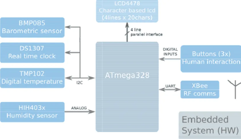
A microcontroller can be programmed using mainly C and assembly languages but some high performance version based on ARM technology can host also Linux operating system. In an embedded system there can be one or more microcontrollers which control other devices of system. In Fig. 1 there is an
example of microcontroller-based embedded system microcontroller is
interfaced with several sensors (humidity, temperature, barometric sensors) and with a Zigbee radio transceiver for wireless communication.
be integrated on a same PCB dual-minimize area, volume and weight.
1.2.2. FPGA-based systems
Another kind of embedded system is based on FPGA devices platform. An FPGA (Field-programmable gate array) circuit which can be configured by a designer
language (HDL). Today FPGAs have large resources of logic gates and RAM blocks to implement complex digital computations. FPGAs can be used to implement any logical function that an ASIC could perform. The ability to update the functionality after shipping offer advantages for many applications.
contain programmable logic components called "logic blocks", and a hierarchy of reconfigurable interconnects that allow the blocks to be
blocks can be configured to perform complex
simple logic gates. In most FPGAs, the logic blocks also include memory elements, which may be simple flip-flops or more complete blocks of memory
possible to see block diagram of a FPGA applications.
Fig. 1 - Example of microcontroller
3
based embedded system, where a single interfaced with several sensors (humidity, temperature, barometric sensors) and with a Zigbee radio transceiver for wireless communication. All these devices can
-layer board using SMD components in order to
Another kind of embedded system is based on FPGA devices which control whole programmable gate array) [4] is an integrated be configured by a designer using a hardware description FPGAs have large resources of logic gates and RAM blocks to implement complex digital computations. FPGAs can be used to implement any logical function that an ASIC could perform. The ability to update offer advantages for many applications. FPGAs components called "logic blocks", and a hierarchy of ts that allow the blocks to be wired together. Logic blocks can be configured to perform complex combinational functions, or . In most FPGAs, the logic blocks also include memory elements, r more complete blocks of memory. In Fig. 2 it is possible to see block diagram of a FPGA-based embedded system for automotive
1.2.3. DSP-based systems
A DSP (Digital Signal Processor) [5] is special microprocessor which is specialized in digital signal processing.Digital signal processing algorithms typically require a large number of mathematical operations to be performed quickly and repeatedly on a series of data samples. Signals are constantly converted from analog to digital, manipulated digitally, and then converted back to analog form. The architecture of a DSP is optimized specifically for digital signal processing. Fig. 3 shows a typical architecture of an embedded smart sensor based on a DSP.
Fig. 2 - Example of FPGA-based embedded system.
5
1.2.4. System on chip (SoC)
A system on chip (SoC) [6] is an integrated circuit which integrates in a single chip all parts of a computer and often other electronic devices (digital, analog, mixed-signal, radio modules, etc). A system based on SoC technology is a typical embedded system. A microcontroller typically is a single-chip system with no much RAM memory, about hundreds of kB, while a SoC can integrate one or more powerful processors (sometimes multi-core) needing to use large external memory chips (Flash, RAM, EEPROM, etc). This kind of system can run operating system such as Linux or Windows.
A SoC is formed typically by:
1. Microcontroller(s), microprocessor(s) or DSP core(s); 2. Graphics or multi-media processor(s);
3. Memory blocks such as ROM, RAM, EEPROM and Flash memory; 4. Timing sources including oscillators and phase-locked loops;
5. Peripherals including counter-timers, real-time timers and power-on reset generators, radio modules;
6. External interfaces such as USB, FireWire, Ethernet, USART, SPI; 7. Analog interfaces including ADCs and DACs;
8. Voltage regulators and power management circuits.
These blocks are connected by either a proprietary or industry-standard bus. SoCs can be fabricated using several technologies such as full custom, standard cell, FPGA, etc. These systems consume less power and have a lower cost and higher reliability than the multi-chip systems that they replace. In Fig. 4 it is shown a SoC Nvidia Tegra 600-series.
2.
DEVELOPMENT OF AN INERTIAL/GPS PLATFORM FOR
MOTION DATA HANDLING
2.1.
Introduction
Nowadays, in many research fields such as body motion recognition (BMR), fall detection (FD), aerial photogrammetry (AP), inertial navigation (IN), etc, there is the necessity to acquire and transmit all body motion parameters (axial accelerations, angular rates, global position, speed, etc) by wireless to a remote host system for control and tracking purposes. The possibility to acquire these motion information in a remote real-time way is more and more requested.
With regard to BMR [7], [8] and FD [9], there are several areas of interest (e.g.: 3D virtual reality, biomedical applications, robotics) in which it is extremely important to detect and recognize all or some human body movements and maybe to reproduce those using a robot. AP [10] and IN [11], [12] fields are older than BMR and FD, but we can find a multitude of different and innovative approaches and applications such as pedestrian navigation in harsh environments [13], agriculture automated vehicles [14], or animal motion analysis [15].
In the market there are several kind of systems which are not general purpose but are highly specialized for a particular application. Some systems use high performance and high cost devices, others are not wireless-based or are too heavy. The main idea is to design a low-cost, complete and flexible system with these features and which can be used for several applications. This system should be compact, portable, lightweight and highly integrated.
2.2.
System design strategy
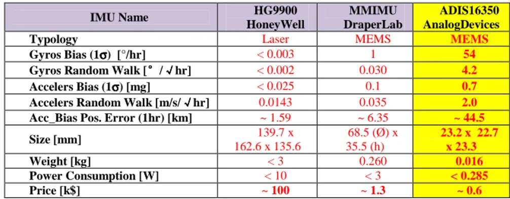
To reach these features it is necessary to design the architecture in a smart way and to select single components in order to save space and to decrease system weight as much as possible. In the first prototype, in order to reduce space and weight, we chose, as inertial sensor, a MEMS inertial measurement unit (IMU) (Analog Devices ADIS16350), constituted by a axial accelerometer and a tri-axial gyroscope. This IMU is a strapdown type system which is intrinsically compact, highly integrated and low-cost but it is not very accurate. In the market
Table 1 - Comparison with commercial IMUs
IMU Name HG9900 HoneyWell MMIMU DraperLab ADIS16350 AnalogDevices
Typology Laser MEMS MEMS
Gyros Bias (1σσσσ) [°/hr] < 0.003 1 54
Gyros Random Walk [°°°°/√√√√hr] < 0.002 0.030 4.2
Accelers Bias (1σσσσ) [mg] < 0.025 0.1 0.7
Accelers Random Walk [m/s/√√√√hr] 0.0143 0.035 2.0
Acc_Bias Pos. Error (1hr) [km] ~ 1.59 ~ 6.35 ~ 44.5
Size [mm] 139.7 x 162.6 x 135.6 68.5 (Ø) x 35.5 (h) 23.2 x 22.7 x 23.3 Weight [kg] < 3 0.260 0.016 Power Consumption [W] < 10 < 3 < 0.285 Price [k$] ~ 100 ~ 1.3 ~ 0.6
7
there are many kind of very high performance IMU but they don't respect our trade-off requirements of low space, weight and cost (Table 1). We designed the system on two different planar boards (main and power boards) using a PCB dual layer-fashion approach. The supply battery packet was reduced to only two rechargeable NiMh AAA batteries. With a reducedbattery packet, the system energy budget is very important to consider. To generate the necessary voltage levels we needed two high-efficiency switching step-up voltage regulators to convert a 2.4V nominal input voltage in two output voltage levels: 5V and 3.3V. In order to handle many motion data, it is important to exploit the available wireless and wired transmission bands organizing data in easily transmissible short packets.
In addition to hardware system side, a remote C-based graphical user interface (GUI) is installed on an Pc-host to control system operations, set inertial sensor parameters (offset, calibration, alignment, etc), display motion variables progress, track trajectories, shoot photo, etc. A trajectory reconstruction algorithm Kalman-based is implemented in the system software for supporting applications such as inertial navigation or motion parameters detection These data elaborations are conducted on software side, instead of hardware side, in order to reduce the computational load of microcontrollers, to speed system operations up and to obtain an easier data handling using the remote GUI.
2.3.
System architecture
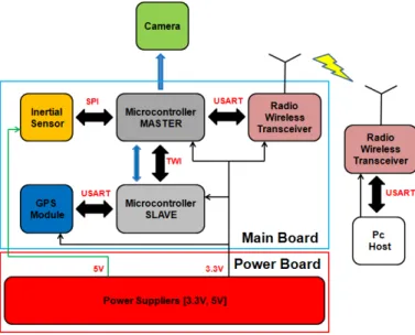
As explained previously, this system is designed on two separated boards: Main Board and Power board. The first manages all control operations, acquiring data from inertial sensor and GPS module, sending data packets to the host pc and receiving command packets from inertial system by wireless; the latter provides the two supply voltage levels to main board.
2.3.1. Power board
The Power board is constituted by two step-up converters (Maxim MAX756) which allow to provide both 5V and 3.3V voltage guaranteeing up to 400mA load current and an efficiency of about 85% (input voltage over 2.2V). As said before, the two rechargeable NiMh battery pack have a nominal voltage of 2.4V and a nominal capacity of about 2650mAh. Considering a nominal input energy of about 6.36Wh against a max required load power of about 625mW (worst case), our system has an autonomy of about 9 hours (experimentally verified).
2.3.2. Main board
The Main board is the control core of whole system. The modules on the board are: two 8 bit microcontrollers (Atmel ATMEGA8) (called Master and Slave), a GPS module (Fastrax UP500), a zigbee transceiver (Maxstream XBEE) and an inertial sensor (AnalogDevice ADIS16350). To support some applications such as aerial or ground photogrammetry, an high resolution camera (Canon SX200IS) was interfaced.Main features of these devices are:
1. ADIS16350: is a low-power (165mW @ 5V) complete inertial measurement station. It is constituted by one tri-axial accelerometer, one tri-axial gyroscope and one tri-axial thermometer for thermal compensation. It transfer inertial data with 14 bit resolution, to the output registers, accessible via a 2MHz SPI interface, at a maximum sample rate of 819.2Hz (350Hz bandwidth). The inertial sensors are precision aligned across axes, and are calibrated for offset and sensitivity.
2. UP500: is a low-power (90mW @ 3V) GPS receiver module with embedded antenna and fix rate up to 5Hz. Communication is based on NMEA protocols, via RS232 link up to 115.2kbps. It supports WAAS/EGNOS correction to improve position resolution up to about 2m.
3. XBEE: is a low-power (165mW @ 3.3V) 2.4GHz transceiver which implements ZigBeeTM protocol and has a transmission range of about 80m. Transmission and reception buffers allow efficient data stream packetization, also required to reach the rated communication speed because every data exchange requires the presence of an about 20 bytes long header. It is interfaced through RS232 protocol up to 115.2kbps.
As we can see in Fig.5, Master microcontroller is connected to ADIS16350 through SPI interface, to XBEE through USART interface, to Slave microcontroller through TWI interface and to the high resolution camera by means of one I/O pin.
The Slave microcontroller is connected only to UP500 by means of USART interface and to Master microcontroller as said before. Another Slave I/O pin is used to send an interrupt to Master when a new GPS frame is ready.Master and Slave are clocked with two 14.7654MHz quartz.
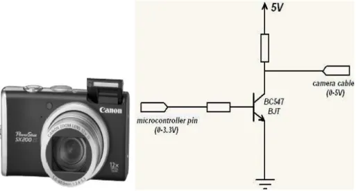
2.3.3. High resolution camera
We used a low-cost 12,1Mpixels Canon SX200IS camera (5-60mm lens focus, 4X digital zoom, 12X optical zoom, shutter speed 1s -1/3200s) (Fig. 6a). The firmware was updated with an unofficial version in order to acquire full control of the camera
9
functions. In particular, we exploited the possibility to remotely shoot photos applying a 3V pulse to the USB port, using a BJT, as in Fig. 6b, and to store photos in uncompressed format (RAW), as required for photogrammetry applications [16]. For georeferencing each picture, a progressive number, corresponding to the file number on the memory card, is recorded on the inertial data frame.
Fig. 6 - Canon SX200i Camera (a), Camera/Microcontroller interfacing (b).
2.4.
System working and data protocol
Thanks to a simple but complete remote GUI, the Pc-host can start every system operation, as will be explained in next sections. There are three kinds of command packets (Fig. 8) that can be sent to the system:
1. operation request (GPS/Inertial data readout, photo shooting, offset readout);
2. configuration setting; 3. configuration readout.
Each command packet is identified by system by means of different opcodes (Fig. 9).
The system requirement was to transmit synchronized data from inertial sensor, operating at 100Hz, and GPS module operating at 5Hz (Fig. 10). This inertial sensor sample rate is important to get a good position resolution in case of trajectory tracking calculations. Hence the data stream has to contain 20 inertial frames plus one GPS frame every 200ms.
The inertial data frame is 20 bytes long and contains the following fields: supply voltage, x/y/z temperatures, x/y/z angular rates, x/y/z linear accelerations. The sensor has to be read by the Master every 10ms and this is guaranteed by a dedicated timer.
The most important problem is constituted by the verboseness of GPS data: in fact, NMEA sentences contain hundreds of bytes. So we had to select only the necessary information, otherwise we were able to reach the specified data rate.
Fig. 8 - Command structure.
11
Because we were not interested in all GPS information, at the start up the Slave initializes the GPS module to send only four sentences:
1. GGA: Global Positioning System Fix Data; 2. GSA: GPS DOP and active satellites; 3. VTG: Track Made Good and Ground Speed;
4. RMC: Recommended Mininum Navigation Information.
These NMEA sentences contain main information which can be useful for several different applications.
Moreover, the Slave creams off the received sentences and stores in RAM only the information to display, i.e. a total of 72 bytes.
Even if reduced in this way, the time required to send such information is still too high (about 6.25ms) in order not to compromise the regularity of the inertial sensor reading.
So we decided to divide the GPS answer in 8 packets of 9 bytes and to send, every 20 ms, two inertial frames plus a GPS packet. So, in 200ms, we send 8 frames of 51 bytes (frame number, 2 inertial frames, 1 GPS packet, photo number) and last 2 frames of 42 bytes (frame number, 2 inertial frames, photo number) as shown in Fig.11.
Data acquired from PC are reconstructed, displayed and stored in a text file for further elaboration; GPS data are also processed at run-time to display the trajectory. The frame number is used to identify each frame within a second (50 frames/s) and is used for:
1. reconstruction of GPS information;
2. identification of any frame lost in reception.
Finally, the Photo number allows for the association of picture files in the SD card with time, position and attitude of the camera.
The complete system protocol is better explained in the flow chart in Fig. 12. Fig. 10 - Inertial/GPS system operations.
Fig. 12 - Data protocol flow chart.
Fig. 11 - GPS/Inertial data timing (in red the GPS data, in green the inertial data).
13
After the reception of a data request from host pc, master microcontroller sends a GPS data request to slave microcontroller and waits for response checking the GPS data ready flag.When slave acquires and creams off a GPS frame it sets the GPS data ready flag so thatmaster starts a 10ms timer up and acquires an inertial frame storing it on RAM. Then master asks slave a single GPS packet which is received on TWI line and immediately stored on RAM. When 10ms timer stops, master acquires a second inertial frame storing it on RAM. In the end master sends the two inertial frames and a GPS packet to XBEE module which sent them to host-pc.When these operations are over, master restarts 10ms timer and begin a new operation cycle. If there is an interruption of GPS operations, master continues to send to host-pc only inertial frames respecting the 10ms timing.
2.5.
Host data handling
2.5.1. Inertial data elaboration
Data acquired from the inertial sensor can be processed to obtain position and orientation of a body and to track a three dimensional trajectory. This technique is called inertial navigation and it is used in a wide range of applications.
Inertial data are processed following the scheme [17] in Fig.13 where:
1. U_acc: signals from accelerometers; 2. U_omega: signals from gyroscopes; 3. a: linear acceleration;
4. v: linear velocity; 5. ω: angular velocity;
6. C: rotation matrix.
The subscripts b denote the body coordinate system (that is the navigation system’s reference frame) while the subscripts n denote the local coordinate system (in which the body move).
The first step of trajectory reconstruction algorithm is the correction of accelerometers and gyroscopes signals. The correction of errors on signals is the most important step of algorithm, because errors influence overall system performance [18]. In particular, propagation of orientation errors caused by noise, perturbing gyroscope signals, is identified as the critical cause of a body position drift. The main cause of errors are: scale factor, bias, drift, temperature, non-orthogonality. In order to compensate them it is necessary to perform a procedure of calibration. A first coarse calibration was executed using the automatic calibration of ADIS16350 managed from remote GUI software. Then a finer calibration was conducted manually. Among all calibration methods proposed in literature, the most appropriate calibration technique for low-cost sensors is the ”modified multi-position calibration method” [19], [20]. Its aim is to find all calibration parameters (bias, scale factor, non-orthogonality, etc) of sensors. It consists in laying out sensors in different linearly independent positions in order to define a system of linearly independent equations which outnumbers the set of calibration parameters to find.
The linear acceleration and angular velocity error can be modeled as:
= + + _ − + 1
= + + _ − + 2
Where:
1. and are the sensor bias;
2. and are the sensor scale factors;
3. _ and _ are the sensor thermal constants;
4. and are the sensor measurement noises, = ∗
! " #! and = ∗ ! " #!, and are noise densities;
5. and are the temperatures during the measurement and at sensor start-up respectively.
In Table 2 there are the calibration parameters obtained according to [19], [22], [23].
15
After the calibration phase, it is necessary to compensate the centrifugal acceleration and the acceleration of gravity effects obtaining accelerations in body coordinate system . The former is compensated subtracting the vector product between angular velocities (from gyroscopes) and linear velocities (from numerical integration of accelerations), the latter is compensated adding the scalar product between transposed rotation matrix and the gravity acceleration. After a numerical integration velocities in body coordinate system are obtained.In order to pass to local coordinate system the linear velocities are multiplied by the rotation matrix and then are integrated to have body trajectory. The angular velocities are also integrated, obtaining the information about the orientation (Euler angles) and the rotation matrix (for transformation from b-frame to n-frame). The equations to integrate and the rotation matrix are [21]:
$% = & _'sin $ + +_'cos $. tan 1 + 2_' 3 1% = & _'cos $ − +_'sin $. 4 5% = & 6sin $ + + +6cos $. sec 1 5
) 6 ( cos cos cos sin sin sin sin cos cos sin sin sin sin cos cos sin cos cos sin cos sin sin cos sin sin sin cos cos cos − + − + + + − =
θ
φ
θ
φ
θ
ψ
θ
φ
ψ
φ
ψ
θ
φ
ψ
θ
ψ
θ
ψ
θ
φ
ψ
φ
ψ
θ
φ
ψ
θ
ψ
θ
n b C Table 2 - Calibration parameters 9:;;_< 0.012133g 9:;;_= 0.023295g 9:;;_> -0.03593g 9?=@A_< 0.3766 °/s 9?=@A_= 0.1963°/s 9?=@A_> 0.6270°/s B:;;_< 0.00775 B:;;_= 0.008838 B:;;_> 0.008041 B?=@A_< 0.004818 B?=@A_= 0.004042 B?=@A_> 0.009385 ;:;;_C 4 mg/°C ;?=@A_C 0.1°/s/°C D:;; 1.85mg √F> D?=@A 0.05°/s √F>where transformation from reference axes to a new frame is expressed as: 1. rotation through angle 5 about reference z-axis;
2. rotation through angle 1 about new y-axis; 3. rotation through angle $ about new x-axis.
However, also with a perfect correction of errors, it isn’t possible to obtain a great position accuracy for long time using only MEMS IMU but it is necessary to include information from GPS module, integrated in our system. Inertial and GPS modules are complementary: the former is characterized by high measurement frequency but short-term accuracy while the second by long-term accuracy but low measurement frequency. The main idea is to reconstruct trajectory by means of inertial data acquired between two GPS acquisitions and then to correct accumulated errors in inertial data using the stable information from GPS module. The Kalman filter is the most used algorithm for this purpose. In literature there are several implementation of Kalman filter depending on the features of devices [3]. To obtain a correct integration of Inertial and GPS data it is important to have high synchronization between data acquisitions. The implementation of Kalman filtering is included into remote GUI.
2.5.2. GPS data handling
In order to plot a GPS trajectory in a two dimensional graph it is necessary at first to transform GPS geodetic coordinates (longitude λ, latitude φ, height h) to ECEF (Earth-Centered-Earth-Fixed) coordinates (Xe, Ye, Ze) and then to NED (Nord-East-Down) coordinates (xn, yn, zn) according to following equations. N(φ) is the normal that is the distance from the surface to the Z-axis along the ellipsoid normal. a is the semi-major ellipsoid axis and e is the first numerical ellipsoid eccentricity. Rn/e is a transformation matrix from ECEF to NED coordinates. Xer, Yer, Zer are ECEF reference coordinates.
2.6.
Remote GUI
The Remote GUI is developed using LabWindows© development environment based on C language. The GUI allows to manage every system operation. As seen in Fig.14 in the window there are three main sections: a graph section to display GPS trajectory, angular velocity and linear acceleration; a boxes section to
λ
φ
φ
λ
φ
φ
λ
φ
φ
cos
cos
)
)
1
)(
(
(
sin
cos
)
)
(
(
cos
cos
)
)
(
(
2h
e
N
Z
h
N
Y
h
N
X
e e e+
−
=
+
=
+
=
)
sin
1
(
)
(
2 2φ
φ
e
a
N
−
=
−
−
−
×
=
er e er e er e e n n n nZ
Z
Y
Y
X
X
R
z
y
x
/
−
−
−
−
−
−
=
φ
λ
φ
λ
φ
λ
λ
φ
λ
φ
λ
φ
sin
sin
cos
cos
cos
0
cos
sin
cos
sin
sin
cos
sin
/ e nR
17
show inertial sensor parameters (supply voltage, x-y-z linear accelerations, angular velocities and temperatures) and GPS parameters (time, latitude, longitude, altitude above mean sea level, height of geoid above WGS84 ellipsoid, speed, heading and PDOP; a command section to initializing XBEE radio-bridge, to start/stop system operations and to shoot photos. It is also possible to save data into a text file for offline analysis. In the top of window there is a menu in which user can access inertial sensor setting mode and manually change gyroscope dynamics, number of tapes of Bartlett FIR digital filter, sample rate, accelerometer ad gyroscope offset or use automatic procedures of axial alignment, offset compensation, calibration (Fig. 15). The numerical integration algorithm, the Kalman filter and the coordinates transformation are integrated into the GUI.
2.7.
System testing
In order to verify proper working of system many kind of tests are conducted on system modules.
2.7.1. Accelerometers/Gyroscopes test
To test accelerometers and gyroscopes, two type of tests were conducted. In the first test, the system was placed on a strobe speed-controlled turntable with velocity of 33 rpm and 45 rpm, to evaluate biases and the correct angular velocity measured by gyroscopes; in the second test, system was placed on a radio-controlled toy car (Fig. 17) and various movements were performed to test the performance of the whole inertial system (Fig.16).
19
2.7.2. GPS module test
Moreover, the system was mounted on a car in order to verify GPS module operations and the coordinates transformation algorithm using GPS data (Fig.14). Another kind of test allows to analyze the proper working of GPS module along a closed path and comparing results with a high accuracy differential GPS module. From this test we valued position errors along x, y and z axis using a statistical
Fig. 16 - Sensor responses for various movements performed (slewing rounds, spins, back/forth).
analysis. In Fig.18 the trajectory comparison between our GPS module and differential GPS module is shown. In Table 3 and Fig. 19 there are the error distribution parameters. The mean position error is lower than 1m for x and y axis with a standard deviation lower than 2m, only for the z axis the mean position error is of about 5m.
21
2.7.3. Inertial-based trajectory reconstruction test
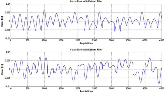
After the GPS trajectory reconstruction test, we conducted an Inertial-based trajectory reconstruction test to verify the quality of trajectory reconstruction algorithm and of Kalman filtering. For this test the strobe speed-controlled turntable was used. As it can be seen in Fig. 20 using just the reconstruction algorithm, after about 25 loop at 33rpm, there is an increasing of offset and bias which deform the circular trajectory with a spiral divergence; with Kalman filtering the trajectory is very stable and it is evident the decreasing of x/y error as shown in Table 4 with respect to Table 5 without Kalman filter. In Fig. 21 the x/y position error fluctuation using the Kalman filter is shown while in Fig. 22 the x/y position error fluctuation without Kalman filter.
Table 3 - Error distribution parameters X-error Mean 0.573m Y-error Mean -0.143m Z-error Mean 4.267m X-error σσσσ 1.825m Y-error σ σ σ σ 1.480m Z-error σσσσ 1.997m Fig. 19 - X/Y/Z error distributions.
Fig. 20 - Trajectory reconstruction without (top) and with (bottom) Kalman filtering.
23
2.8.
Conclusions and future developments
A flexible and low-cost wireless GPS/Inertial system [24] which can be used for many kinds of applications is presented. The main features of prototype are low weight, high compactness, high autonomy, fast remote data managing and elaboration (Table 6). The future developments will be the GPS/Inertial data fusion, the replacement of MEMS sensor station with the new model which integrates a tri-axial magnetometer and an automatic thermal compensation, the replacement of the ZigBee module with the new model having a transmission range up to 1km and assembling all new modules and SMD components on the new PCB dual-layer board (Fig.23) to reduce more and more space and weight in order to increase system flexibility. In addition, the remote system GUI will be modified to manage data elaboration for various applications such as fall detection, body motion recognition, inertial navigation, etc. Many kind of tests in several scenarios will be conducted in order to demonstrate flexibility and general purpose capability of platform.
Table 5 - Error distribution parameters (without Kalman filter)
Abs Max X-error 59.68m Abs Max Y-error 60.57m X-MSE (mean square error) 1.5256e+5m2
Y-MSE (mean square error) 1.4943e+5m2
Fig. 22 - X/Y axis error fluctuations without Kalman filter. Table 4 - Error distribution
parameters (with Kalman filter) Abs Max X-error 0.0066m Abs Max Y-error 0.0084m X-MSE (mean square error) 3.30e-3m2
Table 6 -
Fig. 23 - 3D PCB system board v2.3 image.
Main technical features 3D PCB system board v2.3 image.
25
3.
DEVELOPMENT OF AN EMULATION PLATFORM FOR THE
FF-LYNX PROJECT
3.1.
Introduction
Before describing the topic of this chapter, it is important to introduce the FF-LYNX (Fast and Flexible links) project. This project was promoted and financed by INFN (Istituto Nazionale di Fisica Nucleare), the most important research institute in Italy within the field of High Energy Physics (HEP) experiments. This project, started in January 2009, was born with the first aim to define a new serial communication protocol, to satisfy the typical requirements of HEP scenarios. It was intended to become a new flexible standard within different experiments minimizing development costs and efforts, because today each HEP experiment uses a different kind of custom communication protocol. The second aim of FF-LYNX project was to implement this protocol in radiation-tolerant, low power interfaces. High Energy Physics (HEP), is a branch of physics that studies the most basic constituents of matter, i.e. subatomic particles, and their interactions. Particle accelerators are the main instruments for High Energy Physics. They are complex machines that produce beams of high energy particles. A typical HEP experiment consists in colliding particle beams and analyzing the results of the collisions using particle detectors around the interaction point. Large Hadron Collider (LHC) [25] at CERN (the European Organization for Nuclear Research) in Geneve (Switzerland) is the largest and most powerful particle accelerator over the world.
The electronic architectures used into experiments are very similar with respect to systems for acquisition of data from sensors and for control and management of the detector. Signals generated by sensors in particle detection are handled by Front-End (FE) electronics embedded in the detectors and transferred to remote data acquisition (DAQ) systems. In Fig. 24 a schematic representation of a common HEP experiment.
After a collision between two particles such as two protons, there are the generations of new different particles (collision events) which have to be captured by the detectors that surround the interaction point. These detectors, formed by many high performance sensors (pixels, strips, etc), are interfaced with Front-End (FE) devices that acquire signals and execute a signal conditioning (amplification, shaping, buffering, analog to digital conversion). So these raw digital data organized, in Event Data packets, are stored onto FE memory buffers temporarily. Since the interesting events are a very small fraction of the total, the total amount of data has to be filtered. To do this, a small amount of key information about collision event, in the guise of Trigger packets, is send to TTC (Trigger, Timing and Control) system which performs a fast, approximate calculation and identify if that event is significant or not. If the event is important, then a Trigger command is sent back to FE electronics to command a data readout. At this point, that Event Data packet is sent towards the DAQ (Data Acquisition System). In this way, the amount of data to be transferred is reduced to rates that can be handled by the readout system (a typical order of magnitude is hundreds of MB/s from each FE device), and only the interesting events are selected. Clearly each packet is sent through the communication channel based on different custom protocols.
The part of work presented in this chapter constituted two phases of the FF-LYNX design flow and was carried out at the Pisa division of INFN. It dealt with the simulation of FF-LYNX System-C interface models using a simulation platform and the design of an FPGA emulation platform for verify and test those interface models. In the first phase, these interfaces, defined in System-C language, are simulated using an ISE (Integrated Simulation Environment) platform. In the second phase of work, these interfaces were implemented on FPGA emulation platform to continue the verify process.
3.2.
FF-LYNX protocol basis
The FF-LYNX protocol [26] is a double-wire serial protocol defined at the data-link layer of the ISO/OSI model. The two separate wires correspond to clock and data lines. It guarantees a high level of flexibility as regards data rate and data format. It is possible to communicate with three different data rates: 4xF, 8xF and 16xF, as shown in Fig. 25; F represents the frequency of the reference clock. Considering the LHC reference clock (40 MHz) there are 160, 320 and 640 Mbps respectively. The main feature of FF-LYNX protocol is the time multiplexing of two channels, named THS and FRM. The THS channel is used to transmit Triggers, Frame Headers and Synchronization patterns and employs two bits. The FRM channel is used to transmit data packets (information inserted into one or more data frames as Fig, 26) and employs 2, 6 or 14 bits in the three data rate options. A data packet is a high-level transmission unit which can be formed by several 16bit words. This data packet can fit a single data frame (if packet is formed by less than 16 words) or can be splitted into several data frames. It uses two kinds of data packets: the Variable Latency Frame (VLF) and the Fixed Latency Frame (FLF) packets, where the latency is defined as the data packet transfer time. The VLF is a generic data frame type while the FLF is used as trigger data frame type. The robustness of
27
critical information against transmission errors is obtained by means of Hamming codes and custom encoding techniques.
These techniques guarantee the correct recognition of commands and the reconstruction of their timing in the THS channel. In the FRM channel single bit-flips are corrected and burst errors are detected. There is a significant reduction of the number of physical links thanks to the use of the same protocol for the transmission of triggers, fixed and variable latency reducing the overall material budget. Hence, this protocol is suitable for the distribution both of DAQ signals and of Timing, Trigger and Control (TTC) signals, that is for the Up-Link (Front-End devices to DAQ system) and for the Down-Link (Trigger and Control System to Front-End devices) paths. On the THS channel, Triggers are higher priority signals with respect to Frame Headers and Synchronization commands; these latter can be transmitted only when there are no Triggers for at least three consecutive clock cycles, in agreement with the current specifications of the LHC experiments. On
FRM channel the Data Frames are tagged by Frame Headers transmitted on the THS channel.
Fig. 25 - Channel partitioning through time-division multiplexing (TDM), with the master clock taken as the period for the TDM cycles.
The structure of a data frames is shown in Fig. 26. It is formed by: the Frame Descriptor (FD) which contains information such as the length of the frame and the type of data transmitted, the Label which represents a field that can be employed to add optional information, the Payload which constitutes the user data and a Cycle
Redundancy Check (CRC) that can be optionally applied to the Payload to increase robustness against transmission errors.
In FF-LYNX system, as already mentioned, there are two categories of data with respect to latency constraints, the VLF and the FLF packets: the former have no latency constraints, while the latter must have a fixed latency.
The FF-LYNX protocol is implemented in Transmitter (TX) (Fig. 27.a) and Receiver (RX) (Fig. 27.b) interfaces with a serial port (DAT) on one side and two parallel ports (16-bit port for the VLF packets, 2/6/14-bits port for the FLF ones) with their control (data_valid, get_data, trg) and configuration signals (e.g.: flf_on, label_on) on the
other side. Control signals are used by host devices to manage the data
transmission operations.
The FF-TX Transmitter is constituted of the following modules:
1. TX Buffer: it is structured as two FIFOs, for storing input data on VLF bus and on FLF bus.
Fig. 26 - The basic FF-LYNX frame structure.
29
2. Frame Builder: it controls the assembly of frames for the transmission of data stored in the FLF and VLF FIFOs.
3. THS Scheduler: it works out the arbitration between triggers and frame headers. It receives TRG and HDR commands and passes them to the Serializer avoiding THS sequences overlaps.
4. Serializer: It generates the serial output stream by receiving the Frame Descriptor field from the Frame Builder and frame words from the VLF/FLF FIFO. In addition, it sends TRG and HDR patterns into the THS channel, according to the commands that arrive from the THS Scheduler.
The FF-RX Receiver is constituted of the following modules:
1. Deserializer: It converts the FF-LYNX serial data stream into parallel form. it separates the THS channel and the FRM channel and provides the data words to store into the RX Buffer.
2. THS Detector: It detects the sequences of triggers, headers and synchronization patterns in the THS channel;
3. Synchronizer: It generates the reference clock on the base of information coming from the THS Detector.
4. Frame Analyzer: It controls the reception of data frames, their storing into the RX Buffer and the transmission of stored data to the receiver host.
5. RX Buffer: It buffers data to send to host devices in parallel form.
3.3.
FF-LYNX top-down design flow
As already mentioned, the FF-LYNX project was to follow a well-defined top-down design flow (Fig. 28). This flow consists of six main phases: The protocol definition phase in which the communication interfaces are modeled using System-C language, the high-level validation phase which consists in verify the proper functionality of protocol interfaces employing a simulation platform called ISE (Integrated Simulation Environment), the definition of hardware interfaces using VHDL language, the implementation of interfaces on FPGA devices for the emulation phase and at the end, the design of test ASIC chip implementing these FF-LYNX TX/RX interfaces. In this chapter, mainly the FPGA prototyping phase will be described in detail.
3.4.
FF-LYNX protocol system-C modeling
3.4.1. The ISE (Integrated Simulation Environment) platform
After the theoretical definition of protocol structure, an ISE (Integrated Simulation Environment) platform, based on models written in System-C language [27], was developed. These System-C models describe protocol interfaces, electrical links and I/O test modules with a timing accuracy at clock cycle level. The aim of the ISE platform is to simulate and characterize readout architectures based on FF-LYNX communication protocol, in this case study, with input data compatible with possible working environment in which this protocol could be employed. For this goal, physics GEANT4 input data are used and FoM (Figures of Merit), defined in Table 7, are evaluated.
With this ISE platform it is possible to conduct all kind of analysis in different operating conditions, setting different values of link speed, trigger rate, packet rate, packet average size, bit error rate in electrical serial links. It is possible also to include injection of errors in communication links and memory blocks. All the models that form the ISE are known as "Simulator".
The developed System-C link simulator is composed by two main modules: the FF-LYNX TX interface and the FF-FF-LYNX RX interface. This model architecture is parameterized and modular, allowing the reusability of System-C code and the run-time behavior tuning. This feature is important during the simulation phase when frequent changes in parameter values are needed for FoM estimations.
The Simulator is laid out in a Client/Server architecture (Fig. 29). In the Server side there are two main blocks, the Test Bench and the Server Main modules, while in the Client side there are the Sim Framework and the Client Main modules.
31
Concerning the Server side, the Test Bench module contains the System-C protocol interfaces and its task is to transfer input data from the Server Main to the protocol interfaces and then to receive protocol interface outputs. The Server Main behaves as a functional master module, it stores temporarily both data coming from the Client and data waiting to be transmitted back to it. Both the Server and the Client have a Sim Interface module that interfaces the Server side with the
Fig. 29 - The ISE Client-Server architecture; it can be implemented on SMP (symmetric multi processor) workstation or computing grid.
Table 7 - Figures of Merit (FoM)
Figures of Merit (FoM) Description
Sent Pkt number of VLF packets sent
Lost Pkt number of VLF packets lost
LPR (Lost Packet Rate) Lost Pkt over Sent Pkt
CPDR (Corrupt Packet Descriptor Rate) number of VLF packets received with
incorrect length
CPPR (Corrupt Packet Payload Rate) number of VLF packets received with
damaged payload
Mean, Min, Max PL (Mean, Min, Max Packet Latency)
mean, min and max value of the packet latency
Std PL (Standard Deviation of Packet
Latency) standard deviation of the packet latency
Sent Trg (Sent Triggers) number of triggers sent
Lost Trg (Lost Triggers) number of triggers lost
Lost Hit number of FLF packets lost or corrupted
LTR (Lost Trigger Rate) lost triggers over sent triggers
FTR (Fake Trigger Rate) the rate at which fake triggers are received
Client side. The message passing is implemented on top of TCP/IP sockets. As regards the Client side, the Sim Framework module is made of a Stim_Gen module that generates the stimuli patterns and a FoM_Gauge module that gauges the figures of merit from the simulation results. The Client Main manages their initialization and provides the highway through which data flows from the Sim Interface module to the Sim Framework module and viceversa.
The ISE architecture, being modular, allows to easily change every single module of the system, as long as the module interface remains the same. Thanks to the Client/Server approach there is a high degree of flexibility since the Server side can be relocated on a different (remote) machine or re-implemented for another architecture type (i.e.: FPGA emulator), without modifying the Client side. In this environment a typical simulation is based on one or many "runs" which can have different simulator configurations (parameter settings) to evaluate how the system behaves after these variations. As shown in Fig. 29, the ISE platform can be also implemented both in Symmetric Multi-Processing (SMP) machines (i.e.: multi-core and/or multi-processor) and in powerful computing grids (i.e. hundreds or thousands of processors) by spreading the load on multiple processing units, in order to decrease the simulation time and conduct longer and deeper analysis. An example of a simulation carried out in the ISE environment is shown in Fig. 30 where the packet latency time (mean, max, min and standard deviation metrics) related to VLF data packets varies with the protocol speed (4x, 8x, 16x). For this analysis the physical layer considered is a coaxial cable. In Fig. 31 and 32 there are two examples of performance analysis that can be carried out, since the early protocol development steps, by using the ISE platform.
The analysis in Fig. 31 and 32 regards the evaluation of mean sync time and false sync percentage for different values of the N_unlock and of the N_lock thresholds used in the Synchronization module of the FF-RX interface. Sync time, expressed in 40 MHz reference clock cycles, is the time for system re-synchronization after a synchronization loss, while false sync percentage depends on fake synchronization events. N_unlock and N_lock are thresholds that indicate the minimum number of detected synchronization sequences on one of the possible THS channels (4, 8 or 16 in the three speed options) for synchronization unlocking and locking respectively. The synchronization mechanism is based on the counting of THS sequences in each channel and the reaching of two counting thresholds (a high threshold, N_lock, and a low one, N_unlock) was chosen to distinguish a synchronization lock state (when synchronization is considered as acquired) and an out-of-lock state (when synchronization is being looked for).
33
Fig. 30 - Mean, minimum, maximum and standard deviation of packet latency with different link speeds.
Fig. 31 - Mean synchronization time for different threshold settings.