wave excitation from pinned
magnetic domain walls
Ben Van de Wiele
1, Sampo J. Hämäläinen
2, Pavel Baláž
3, Federico Montoncello
4&
Sebastiaan van Dijken
2Miniaturization of magnonic devices for wave-like computing requires emission of short-wavelength spin waves, a key feature that cannot be achieved with microwave antennas. In this paper, we propose a tunable source of short-wavelength spin waves based on highly localized and strongly pinned magnetic domain walls in ferroelectric-ferromagnetic bilayers. When driven into oscillation by a microwave spin-polarized current, the magnetic domain walls emit spin waves with the same frequency as the excitation current. The amplitude of the emitted spin waves and the range of attainable excitation frequencies depend on the availability of domain wall resonance modes. In this respect, pinned domain walls in magnetic nanowires are particularly attractive. In this geometry, spin wave confinement perpendicular to the nanowire axis produces a multitude of domain wall resonances enabling efficient spin wave emission at frequencies up to 100 GHz and wavelengths down to 20 nm. At high frequency, the emission of spin waves in magnetic nanowires becomes monochromatic. Moreover, pinning of magnetic domain wall oscillators onto the same ferroelectric domain boundary in parallel nanowires guarantees good coherency between spin wave sources, which opens perspectives towards the realization of Mach-Zehnder type logic devices and sensors.
Collective spin wave excitations in ferromagnetic materials provide a promising platform for low power wave-like computing in nanoscale devices up to THz frequencies1–3. Several concepts and building blocks for spin wave
technologies have been developed in recent years, including magnonic crystals4,5, logic gates6–8, transistors9, and
multiplexers10. Spin wave emission is an essential part of all these structures. Electrical excitation of spin waves
in ferromagnetic materials is conventionally realized by the use of a microwave antenna. One of the drawbacks of this approach is the impossibility to efficiently excite spin waves with wavelengths that are shorter than the antenna width11, limiting the downscaling of devices. Motivated by this shortcoming, alternative approaches
for the emission of short-wavelength spin waves have been explored recently. Examples include the design of wavelength conversions in the vicinity of microwave antennas using tapered waveguides12 or magnetic grating
couplers13, the use of resonantly driven microwave-to-spin-wave transducers14, and the injection of spin waves
from spin-torque nano-oscillators15–18. Topological defects in ferromagnetic films such as vortices and domain
walls provide another attractive route towards the realization of localized spin-wave sources19. When brought
into oscillation, the non-collinear spin structure of a defect induces regular magnetic perturbations that prop-agate through the ferromagnetic layer as spin waves. If the lateral size of the topological defect is small and its oscillation amplitude is restricted by a strong pinning potential, the wavelength of the emitted spin waves can be extremely short.
In this work, we propose a highly tunable source of short-wavelength spin waves based on strongly pinned oscillating domain walls in a ferromagnetic-ferroelectric bilayer. In particular, we consider ferromagnetic films that are strain-coupled to a ferroelectric BaTiO3 layer, but the concept can be extended to other ferroelectric
materials and magnetoelectric coupling mechanisms. Strain-coupling between the ferroelectric and ferro-magnetic layer originates in the transfer of in-plane lattice tetragonality from the ferroelectric domains to the
1Department of Electrical Energy, Systems and Automation, Ghent University, Technologiepark 913, B-9052 Ghent,
Belgium. 2NanoSpin, Department of Applied Physics, Aalto University School of Science, P.O. Box 15100, FI-00076
Aalto, Finland. 3Department of Condensed Matter Physics, Charles University, Ke Karlovu 5, 121 16 Prague, Czech
Republic. 4Dipartimento di Fisica e Scienze della Terra, Università degli Studi di Ferrara, Via Saragat 1, 44122 Ferrara,
Italy. Correspondence and requests for materials should be addressed to B.V.d.W. (email: ben.vandewiele@ugent. be) or S.v.D. (email: [email protected])
received: 26 August 2015 accepted: 18 January 2016 Published: 17 February 2016
ferromagnetic material, leading to modulations of magnetic anisotropy via inverse magnetostriction. While other domain patterns are also suitable, the ferroelectric layer considered in this paper consist of a regular repetition of
a1- and a2 stripe domains. This domain pattern is characterized by abrupt 90 degree rotations of the ferroelectric
polarization and lattice tetragonality in the film plane. Because of strain coupling, uniaxial magnetic anisotropy is induced in the ferromagnetic film that covers the alternating a1- and a2 stripe domains. The orientation of the
uniaxial magnetic anisotropy follows the lattice tetragonality in the ferroelectric layer, i.e. it rotates by 90 degrees at domain boundaries. The regular modulation of magnetic anisotropy in the ferromagnetic film leads to full domain pattern transfer from the ferroelectric layer, an effect that has been experimentally demonstrated for various magnetic materials on BaTiO320–23. A schematic illustration of the ferroelectric-ferromagnetic bilayer in
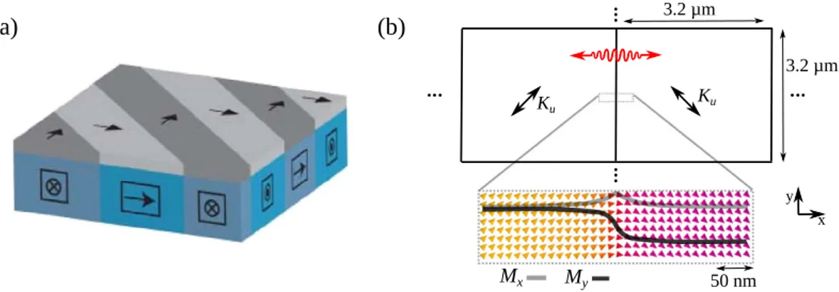
zero magnetic field is shown in Fig. 1. Besides the formation of regular magnetic stripe domains, strong magnetic domain wall pinning on top of perfectly straight ferroelectric domain boundaries is another key attribute of the hybrid material system. Since the ferroelectric boundaries are only a few nanometers wide24,25, the strain-induced
90 degree rotations of uniaxial magnetic anisotropy occur nearly instantly. This effect leads to strong and highly localized pinning of straight magnetic domain walls and enables the emission of short-wavelength spin waves.
To analyze spin wave excitation from a pinned magnetic domain wall and the propagation of these waves in the ferromagnetic domains, micromagnetic simulations are performed. The domain wall is excited by an ac spin-polarized current26,27, which via the spin-transfer torque effect results in driven domain wall oscillations in
a narrow harmonic pinning potential. Regular back-and-forth motion of the magnetic domain wall leads to the emission of spin waves with corresponding frequency. Variation of the driving frequency enables versatile tuning of the spin wave wavelength from the micrometer length scale down to about 100 nm in continuous ferromag-netic layers. Monochromatic excitation of spin waves with even shorter wavelengths is realized by patterning of the ferromagnetic film into magnetic nanowires.
Results
Micromagnetic simulations are performed using MuMax328 (see Methods for details). The simulation geometry,
which is restricted to a 6.4 × 3.2 μm2 region with an a
1 and a2 domain, is shown in Fig. 1(b). Periodic boundary
conditions are applied in both the x- and y-direction to mimic stripe domains with infinite stripe length (along y) and a width of 3.2 μm. Strain coupling to the ferroelectric layer is implemented by a magnetic anisotropy (Ku) and abrupt 90 degree rotation of the uniaxial anisotropy axis at the a1 − a2 domain boundary. Simulations are
per-formed for zero applied magnetic field after initialization of a head-to-tail magnetization configuration in the ferromagnetic domains (Fig. 1(a)). The width of the magnetic domain walls is of the order 10–100 nm, depending on magnetic anisotropy strength. Abrupt rotation of the magnetic anisotropy boundary ensures strong pinning of perfectly straight magnetic domain walls, in agreement with experimental observations20–23. The domain wall
oscillations and spin waves that we consider in this paper only correspond to small perturbations δ ( , )m r of the t
equilibrium magnetization state ( )m r0 . Since the effects of such small δ ( , )m r on the polarization state in the t
ferroelectric layer are negligible, it is possible to simulate the main physical phenomena by considering the ferro-magnetic layer only.
Magnetic domain wall oscillations.
The magnetic domain wall can be described as a quasiparticle that is trapped by a pinning potential. To characterize domain wall pinning under dynamic excitation, we consider a 15 nm thick ferromagnetic layer with saturation magnetization MS= . ×1 7 106 A/m and exchange constantFigure 1. (a) Schematic of the ferroelectric-ferromagnetic bilayer structure. The polarization of the
ferroelectric a1 and a2 domains is aligned along the elongated in-plane axis of the tetragonal BaTiO3 lattice and
it rotates by 90 degrees at the domain boundaries. Via strain transfer and inverse magnetostriction, uniaxial anisotropy is induced in the ferromagnetic layer. The resulting ferromagnetic domain pattern fully correlates with the ferroelectric domain structure and magnetic domain walls are strongly pinned onto the ferroelectric domain boundaries by abrupt 90 degree rotations of magnetic anisotropy. (b) Micromagnetic simulation geometry for an extended film. The computational area is restricted to one period of the stripe domain structure, i.e. a single a1 and a2 domain, both having a width of 3.2 μm. Periodic boundary conditions in the x-
and y-direction are used to account for the continuous film geometry. The simulated magnetization pattern near the magnetic domain wall is shown as inset.
= . × −
Kex 2 1 10 11 J/m. These values correspond to recent experiments on strain-coupled CoFe films on BaTiO320,21. The resonant frequency of the pinned domain wall is determined by the application of 1 ns
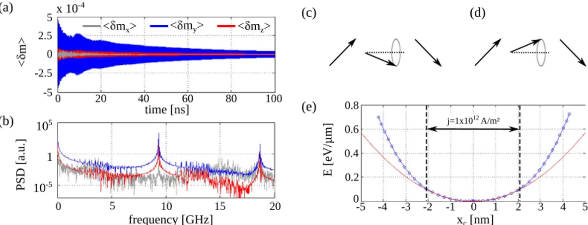
rectangu-lar spin-porectangu-larized current pulses with density ×5 1012 A/m2 perpendicular to the domain wall and simulation of
the dynamic magnetic response for a subsequent period of 0.1 μs. Via the spin-transfer-torque effect, the current pulses affect the non-uniform magnetization profile of the magnetic domain wall. The time evolution of the per-turbations δm averaged over a 400 nm wide region around the domain wall and the corresponding power spec-trum densities (PSDs) are plotted in Fig. 2(a,b). In these simulations, Ku= ×5 104 J/m3. The PSDs of the averaged magnetization components δ〈 my〉 and δmz clearly evidence the presence of a resonance at fres
= 9.33 GHz. Since the resonance peak is significantly smaller in the PSD of δmx , the dynamic mode corresponds
to local magnetization precession around the x-axis, i.e. perpendicular to the domain wall, as illustrated in Fig. 2(c,d). This rotation of magnetization inside the domain wall corresponds to a damped back-and-forth motion of the wall. Higher harmonics of this oscillation mode are also present, as indicated by the resonance peaks at = ×f 2 fres in the PSDs of Fig. 2(b).
To quantify the pinning potential, a microwave spin-polarized current with =f fres and gradually increasing amplitude is applied perpendicular to the magnetic domain wall. This actuation scheme results in driven domain wall oscillations at the same frequency and increasing oscillation amplitude (see Methods for details). For this dynamic resonance mode, the shape and magnitude of the domain wall pinning potential is determined by the dependence of the system’s potential energy on the position of the wall. A result for Ku= ×5 104 J/m3 is shown in Fig. 2(e). Here, the position of the domain wall center xc (defined as ( ) =m xy c 0) is plotted every time the
domain wall reaches the maximum displacement. From the data, a potential stiffness of κ = 7.11 × 10⁻³ J/m2/μm
is extracted by fitting a parabolic energy profile E= /1 2κxc2 to the simulated curve. Only for small domain wall
displacements excited with current densities ≤ ×j 1 1012 A/m the oscillator is harmonic. A domain wall mass is
derived from Mass = κ/(2πfres)2. For the data in Fig. 2 this results in a mass of . ×2 07 10−24 kg per μm length of
the magnetic domain wall. This value is in line with domain wall masses of 6.6 × 10⁻²³ kg, 2.3 × 10⁻²² kg, and
1.3 × 10⁻²⁴ kg, measured on 45 nm × 70 nm, 20 nm × 400 nm, and 20 nm × 2μm wide Permalloy nanowires,
respectively26,29,30. Moreover, good fits of the domain wall magnetization profile are obtained using
π
( ) = / ( /∆)
m xy 2 arctan x (see Fig. 1). The fitting parameter Δ in this equation is proportional to the domain wall width.
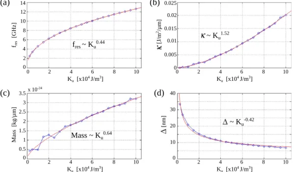
Using the same methodology, we determined the resonance frequency, potential stiffness, domain wall mass and Δ for different anisotropy strengths Ku. In practice, the latter can be controlled by tuning of the magnetoelas-tic properties of the ferromagnemagnetoelas-tic material or variation of the coupling efficiency to the ferroelectric layer. The numerical results, which fully quantify the properties of the magnetic domain wall oscillator, are summarized in Fig. 3. For decreasing Ku, both the domain wall and the pinning potential broaden. Here, =K 0u is a singularity as it represents decoupling between the ferromagnetic and ferroelectric layers. In this case, no magnetic domains and domain walls are present and the mass and resonance frequency are zero. The fitted power behaviors agree well with the predictions of a 1-dimensional model that we developed for a pinned 90 degree magnetic domain wall: f ∼K /
res u1 2, κ ∼Ku3 2/, Mass ∼ Ku1 2/, and ∆ ∼Ku− /1 2 (see Methods).
Spin wave emission.
When magnetic domain wall oscillations are excited by a microwave spin-polarized current, energy is continuously pumped into the system. During each excitation cycle, the amount of energy furnished to the system is dissipated by the emission of spin waves and internal damping. To investigate the prop-erties of the spin waves, we performed simulations using a sinusoidal spin-polarized current with frequency fFigure 2. (a) Time evolution of the magnetic pertubation δ ( )m averaged over a 400 nm wide region around t
the domain wall after the application of a 1 ns current pulse. (b) PSDs of the curves presented in (a). (c,d) Sketch of magnetization precession inside the domain wall. At resonance, the magnetic domain wall oscillates back and forth (displacement to the left in (c) and to the right in (d)). (e) Shape of the pinning potential. Symbols are numerical data and the red line is calculated using E= /1 2κxc2, with κ and xc indicating the domain wall
stiffness and wall displacement along the x-axis. For current densities > ×j 1 1012 A/m2, the pinning potential
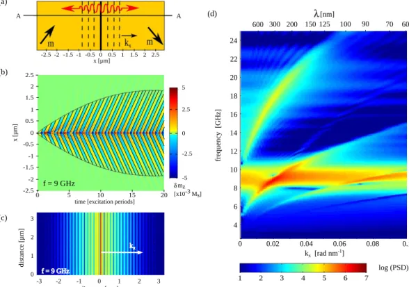
and a density of = ×j 1 1012 A/m2. Because of the infinite length of the magnetic domain wall, the emitted spin
waves propagate perpendicular to the domain wall despite the 45 degree angle between the magnetization of the domains and wave vector kx (see next section for more information). In other words, the wave fronts of the spin
waves are parallel to the domain wall, as illustrated in Fig. 4(a). Figure 4(b) shows how spin waves with =f 9 GHz propagate into the ferromagnetic domains. The solid black lines denote the location of spin wave nodes. They illustrate how the two nodes that are generated during each excitation period propagate away from the domain wall. The slope of the lines corresponds to the phase velocity of the spin waves. The dotted lines in Fig. 4(b) indi-cate the distance from the magnetic domain wall at which the spin wave amplitude drops below 0.15 × 10⁻³ M
S.
While this envelope is initially determined by the product of phase velocity and time, it converges to a constant value after about 15 excitation periods. Beyond this excitation time, the energy that is continuously pumped into the system by microwave excitation of the oscillating domain wall is balanced by energy dissipation through intrinsic spin wave damping31. The out-of-plane magnetization profile after 20 excitation periods is shown in
Fig. 4(c). From such a profile, the wave-vector spectrum at excitation frequency f can be extracted by a spatial (1D) Fourier transformation, i.e. ( ( , =x m x tz 20T)). By repeating this simulation approach for different fre-quencies, a full dispersion diagram ( −f kx) is obtained. A result for Ku= ×5 104 J/m3 and frequencies ranging
from 2.5 GHz to 25 GHz is shown in Fig. 4(d). Various dispersion bands are observed. The broad horizontal and thus non-dispersive band around = .f 9 3 GHz corresponds to the fundamental domain wall oscillation mode. To interpret the other dispersive spin wave bands, the anisotropic nature of spin wave propagation in ferromagnetic domains needs to be taken into account. This is the topic of the next section.
Characterization of spin wave propagation.
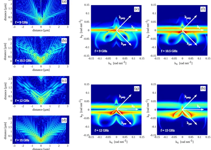
Spin wave properties depend sensitively on the angle between the wave vector and the direction of magnetization. In most studies, large magnetic bias fields are used to saturate the magnetization throughout the sample. Two main propagation modes are often considered, namely parallel (backward volume spin waves) and perpendicular (surface spin waves) to the magnetization. In the fer-romagnetic domains of the hybrid bilayer that we consider, the remanent magnetization direction is set by the uniaxial magnetic anisotropy. The oscillating domain wall emits spin waves at an angle of 45 degrees with respect to this magnetization direction. To obtain further insights in the propagation of spin waves inside the ferromag-netic domains, we interpret the domain wall emitter as a line source that consists of an infinite amount of point sources. Each point along the oscillating domain wall emits spin waves which interfere to an overall spin wave pattern following the Huygens-Fresnel principle. In the following simulations, we analyze the anisotropic propa-gation properties of spin waves that are emitted from a point-like source by exciting the magnetic domain wall over a length of only 50 nm. Magnetization profiles after 20 excitation periods are shown in Fig. 5 for different frequencies and Ku= ×5 104 J/m3 along with their two-dimensional (2D) wave-vector spectra( =k kx xe +ky ye), which are obtained by a 2D spatial Fourier transformation of the magnetization profiles, i.e.
( ( , , =m x y t 20T))
xy z
.
The simulations reveal that spin waves propagate along the domain wall and into the ferromagnetic domains. At =f 9 GHz (Fig. 5(a)), the magnetization along the entire domain wall oscillates in phase. The wavelength of
Figure 3. (a–d) Resonance frequency fres, potential stiffness κ, magnetic domain wall mass, and domain wall fitting parameter Δ versus magnetic anisotropy strength Ku. While the data points represent numerical data,
the full lines are best fits ∼y Ka
the spin waves propagating along the wall is thus infinite and =ky 0. This oscillation mode corresponds to the fundamental resonance of the pinned domain wall. At higher frequencies (Fig. 5(b–d)), nodal lines appear along the domain wall, indicating a decrease of spin wave wavelength and thus an increase of ky. In reciprocal space,
spin waves that propagate along the domain wall are reflected by horizontal bands (Fig. 5(e–h)), one at =ky 0 for =
f 9 GHz and two symmetric bands at | | ≠ky 0 for higher excitation frequencies.
Spin wave propagation into the ferromagnetic domains is highly anisotropic (Fig. 5(a–d)). It is most efficient perpendicular to the local magnetization, i.e. for surface spin waves. In this direction, the wavelength of the spin waves and their decay length are relatively large. At the same frequency, spin waves that propagate parallel to the magnetization (backward volume spin waves) have shorter wavelength and they are attenuated more quickly. With increasing excitation frequency, the wavelengths of both types of spin waves decrease. These observations are also illustrated by the reciprocal space plots of Fig. 5(e–h). The highly anisotropic nature of spin wave propa-gation inside the ferromagnetic domains is reflected by the congruent shapes of the isofrequency contours. The contours with large wave vector in the third and fourth quadrant correspond to modes with small angles between the wave vector and local magnetization, whereas the first and second quadrant depict modes with large angles. The congruency of the modes and the periodicity in reciprocal space ( ( ) = × ( )kn f n k0 f (with n an integer))
suggests that modes with kn 0> ( )f are higher harmonics of the spin wave mode characterized by ( )k0 f .
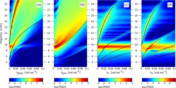
We now consider three specific spin wave propagation directions; parallel and perpendicular to the magneti-zation inside the domains and perpendicular to the magnetic domain wall, which are indicated by kpar, kperp and
kx in Fig. 5. A dispersion diagram for each of these spin wave modes is constructed by combining simulation data
with different excitation frequency. The results are shown in Fig. 6 (a–c). For further analysis of the spin wave properties, we use the theoretical model of ref. 32 to calculate spin wave dispersion curves for arbitrary angles φ between the wave vector and local magnetization. In this model, the 0th order approximation for ω (= πf2 ) is given by ω2=ω ωex( ex+ωMF). ( )1 Here φ ω ω φ = − + ( − ), ( ) F 1 Pcos P1 Psin 2 M ex 2 2
Figure 4. (a) Schematic illustration of spin wave emission from an infinitely long oscillating domain wall. The
wave fronts of propagating spin waves in the domains are parallel to the domain wall. (b) Spin wave profiles along line A in panel (a) as a function of excitation time. Solid black lines indicate the location of spin wave nodes. Dotted lines denote the location where the spin wave amplitude drops below 0.15 × 10⁻³ M
S. The excitation
frequency is 9 GHz. (c) Logarithmic plot of the spin wave profile after 20 excitation cycles. (d) Dispersion graph of the emitted spin waves after 20 excitation periods. All data were obtained for Ku= ×5 104 J/m3.
= − − (− ), ( )
P kd
kd
1 1 exp 3
d is the sample thickness, ω =ω + ω
µ k
K
M M
ex 0 2 ex 2
0 s2
, ωM=γµ0MS, and ω0=γµ0 0H. H0 is the total internal field,
which corresponds to the anisotropy field in our system. The numerically obtained dispersive branches are indi-cated by solid lines in Fig. 6. A good match between theory and micromagnetic simulations is obtained for
ω0=2πfres, with fres the resonance frequency of the domain wall oscillator. The low-intensity dispersion branches correspond to harmonics ( ) = ( )/f kn f k n1 (with n an integer), which originate from the congruent isofrequency contours in reciprocal space. The dispersion diagram for spin wave propagation along the x-direction (Fig. 6(c)) contains identical branches as that of Fig. 4(c), which is replotted in Fig. 6(d) for direct comparison. In the latter, the domain wall was excited over its complete length. In the Huygens-Fresnel interpretation, this means that all point sources along the domain wall interfere such that only waves with =ky 0 contribute constructively to the resulting spin wave pattern. In addition to these branches, the non-dispersive band centered around the domain wall resonance frequency is also observed.
Discussion
The thin-film domain wall oscillator that we described thus far generates spin waves with wavelengths down to
λ =150 nm and frequencies up to f = 24 GHz (see Fig. 4(d)). At higher frequencies, the magnetic domain wall can no longer follow the microwave excitation signal and spin wave emission into the extended film is drastically diminished. Many magnonic devices, however, rely on the ability to excite and guide spin waves through pat-terned geometries, in particular magnetic nanowires. In most devices, spin waves are generated by microwave antennas and large magnetic bias fields are utilized to saturate the magnetization, guaranteeing uniform propaga-tion along the wire. To investigate how such a nanowire geometry affects spin wave emission from a pinned
Figure 5. (a–d) Logarithmic plots of the spin wave profile after local excitation of the domain wall over a length
of 50 nm with a sinusoidal spin-polarized current. The plots in (a–d) are obtained for an excitation frequency of 9 GHz, 10.5 GHz, 12 GHz, and 15 GHz, respectively. (e–h) Corresponding reciprocal space plots. The horizontal bands represent spin waves that propagate along the domain wall. Other isofrequency contours with wave vectors =k kx xe +ky ye indicate spin waves that propagate into the ferromagnetic domains. In all plots, the
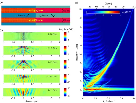
magnetic domain wall in a ferroelectric-ferromagnetic bilayer, we performed additional micromagnetic simula-tions. The main findings for two parallel nanowires with a width of 400 nm and a ferromagnetic film thickness of 15 nm are summarized in Fig. 7. The magnetization in the nanowires is fixed by strong coupling to the ferroelec-tric layer (Ku= ×5 104 J/m3), which makes the application of a bias field superfluous. The dispersion diagram of Fig. 7(b) contains several interesting features. The amplitude of the excitation current is set to = ×j 5 1012 A/m2
to increase the spin wave signal. Similar to the extended film geometry, a broad non-dispersive band is obtained around f = 11 GHz. As discussed before, this mode stems from resonant back-and-forth motion of the magnetic domain wall. Because of the finite nanowire width, however, additional domain wall resonances appear at higher frequencies. Since the magnetization in the center of the domain wall is oriented perpendicular to the wall, the new modes correspond to Damon-Eshbach-like standing waves (DE modes), i.e. surface spin waves excited in the magnetic domain wall (see Fig. 7(c)). The resonance modes are characterized by the number of nodes along the domain wall at =x 0. The resonance at 11 GHz can thus be interpreted as the 0th-DE resonance, while higher order resonances at 14.5 GHz, 17 GHz, 21.5 GHz and 25 GHz in the dispersion diagram of Fig. 7(b) can be labeled as 1st-DE, 2nd-DE, 3rd-DE and 4th-DE modes. At resonance, the relation between the standing wave wavelength (λn) of the nth-DE mode and the nanowire width (w) is given by λ =n n 2w. The energy that is efficiently absorbed
from the microwave current under these matching conditions is dissipated by the domain wall oscillator via the emission of large-amplitude spin waves into the nanowire. For ( ≤n 5), the excitation of spin waves by the differ-ent DE modes produces separate bands in the dispersion diagram of Fig. 7(b). Yet, at larger wave vector and fre-quency, the dispersion of emitted spin waves by higher order DE modes converges onto a single curve. From the slope of this curve, a large spin wave group velocity of = /vg f kx ≈ 2000 m/s is inferred.
Most interestingly, the dispersion diagram evidences that the implementation of a domain wall oscillator in a magnetic nanowire allows for the emission of short-wavelength spin waves at high frequencies. For example, the wave vector of propagating spin waves at an excitation frequency of f = 50 GHz in Fig. 7(b) corresponds to
λ = 25 nm. The reason for these attractive emission properties is twofold: (i) Contrary to the extended film geom-etry, higher order domain wall resonances exist at high frequency because of spin wave confinement perpendic-ular to the nanowire axis. As a result, large-amplitude spin waves are emitted into the nanowire over a wide range of excitation frequencies. The spin wave profiles of Fig. 7(c) clearly illustrate this. At f = 50 GHz, for instance, the 12th-DE resonance mode generates short-wavelength spin waves that propagate into the nanowire over several micrometers. (ii) The second key feature of the magnetic domain wall oscillator is its straight and narrow excita-tion area, which is provided by strong pinning onto the few nanometers wide a1 − a2 domain boundary in the
ferroelectric layer. The uniformity of the pinning potential is thus not limited by the resolution of a lithography process. These important attributes and the absence of long-range magnetic bias fields open up perspectives towards the development of miniaturized magnonic devices. In such sub-micrometer magnonic elements, damp-ing of spin waves is no longer a limitdamp-ing factor, while large group velocities guarantee fast signal throughput in a broad GHz frequency range.
Figure 6. (a–c) Spin wave dispersion diagrams obtained by exciting the magnetic domain wall over a length of
only 50 nm. Spin waves with wave vectors =k kperp (surface spin waves), =k kpar (backward volume spin
waves) and = kk x xe are considered. The black lines in panels (a–c) are numerically calculated using φ= /π 2,
φ =0, and φ= /π 4, respectively, in equation (1). Harmonics are also included. (d) Dispersion diagram for spin waves that are generated by excitation of the entire magnetic domain wall (the data are identical to those of Fig. 4(d)).
An important feature of the nanowire oscillator is the monochromatic nature of excited spin waves at high fre-quency. For instance, the wave vector line width at f = 50 GHz is δk ≈ 0.01 rad/nm, which corresponds to a wave-length distribution of only δλ ≈ 1 nm. Moreover, domain wall oscillators in parallel nanowires that are pinned onto the same ferroelectric domain wall (Fig. 7(a)) emit spin waves with identical dispersion properties. Thus, when the same microwave current is fed into multiple wires, the spin wave sources will emit coherently. If desired, fixed phase relations between propagating spin waves in different nanowires can be attained by tuning the phase of the individual excitation signals. Monochromatic and coherent emission of spin waves from different sources can be used to realize Mach-Zehnder type logic elements and sensors6,33,7. Also, because ferroelectric domains
are separated by parallel and perfectly straight domain boundaries it is possible to define identical domain wall oscillators in one-and-the-same magnetic nanowire (contrary to the single oscillator in Fig. 7(a)). Such coherent spin wave sources would allow for the engineering of magnonic band gaps without additional patterning34, again
alleviating lithographic restrictions.
To summarize, based on micromagnetic simulations, we have proposed a highly tunable source of short-wavelength spin waves. The source consists of a pinned magnetic domain wall that is strain-coupled to a straight and narrow domain boundary in a ferroelectric layer. Oscillations of the magnetic domain wall in the highly localized pinning potential are driven by a microwave spin-polarized current via the spin-transfer torque effect. The energy that is continuously pumped into the domain wall oscillator is dissipated by internal damping and the emission of spin waves at the same frequency as the excitation signal. The properties of the spin wave source depend on the domain wall resonance modes, which can be engineered by patterning of the ferromagnetic layer. In magnetic nanowires, the fundamental back-and-forth oscillation mode is complemented by multiple resonances that are caused by Damon-Eshbach-like standing waves inside the domain wall. As a consequence, pinned domain walls in magnetic nanowires allow for spin wave emission up to about 100 GHz. The wavelength of the excited spin waves at high frequency is uniquely defined (monochromatic emission) and short, typically 10-100 nm, opening new avenues for the realization of nanoscale magnonic devices.
Methods
Micromagnetic simulations.
The time evolution of the magnetization m in the ferromagnetic layer is gov-erned by the Landau-Lifshitz-Gilbert equation35 with additional spin-transfer-torque terms to account for theeffect of a current density j36
Figure 7. (a) Schematic of spin wave excitation and propagation in two parallel magnetic nanowires on top
of a ferroelectric layer with an a1 and a2 domain. Small arrows indicate the direction of magnetization in zero
magnetic field. (b) Dispersion graph of propagating spin waves in the nanowires. (c) Spin wave profiles for several resonance frequencies of the domain wall oscillator. The profiles are a superposition of spin waves generated by the corresponding nth-DE resonance mode at the excitation frequency and some lower order DE modes.
with an extended film geometry, periodic boundary conditions are applied in both the x- and y-directions. For the magnetic nanowire, this is only done in the x-direction. In all simulations, a large damping constant of α = 1 is used in the outer left and right 400 nm wide regions of the simulation area to exclude interference with spin waves that are generated by other domain walls. In the central part of the simulations, α is adjusted to give the best pos-sible analysis of different spin wave properties: to determine fres with optimal resolution we used α =10−4,
which resulted in large spin wave signals on a 100 ns time scale (see Fig. 2(a)); to ensure that all energy increases in Fig. 2(e) can be attributed to oscillations of the magnetic domain wall, we instantly damped the emitted spin waves using α = 1; to compute the spin wave dispersions, we used a physically realistic damping parameter of
α = .0 015.
To calculate the stiffness of the pinning potential, a sinusoidal current density profile with gradually increasing amplitude, j t( ) = . ×0 1 1012f tres sin 2( πf tres ), is applied to the domain wall. Here, f
res is the resonance
fre-quency of the domain wall oscillator. This actuation scheme results in driven domain wall oscillations with increasing amplitude. The domain wall displacement is collected at every = ( + ) /t 2n 1 T 4, with = /T 1 fres and
n an integer. This is when the domain wall displacement is maximal and the domain wall velocity is zero. This way,
dynamic energy contributions due to domain wall tilting at non-zero domain wall velocities do not affect the data. The obtained energy versus displacement relation ( −E xc) can be fitted by E= /1 2κxc2, where κ is the potential
stiffness.
For the simulation of the dispersion graphs of the thin-film geometry, Figs 4(d) and 6(d), a current density = ×
j 1 1012 A/m2 is imposed to the ferromagnetic layer, which is in the linear region of the oscillator (see
Fig. 2(e)). For all other simulations, a higher current density of 5 × 10¹² A/m2 is imposed. Tests on the thin-film
geometry indicate that the use of this higher current density results in an increased power density, but that the anharmonic potential does not excite non-linear spin wave modes. The high current densities are motivated by numerical arguments. The Graphics Processing Units hardware that was used in this work has a 6-digits resolu-tion. As a result, magnetic perturbations of δ >m 10−5 M
S can be resolved. As the emitted spin waves are still
linear perturbations, the spin wave intensity scales down linearly with decreasing current density. Less intense spin waves can easily be measured using available experimental techniques37,38.
Model of 90 degree magnetic domain wall oscillator.
In addition to micromagnetic simulations, we developed a 1-dimensional model to describe the driven oscillations of a 90 degree magnetic domain wall. Again, we consider an anisotropy boundary at =x 0. In the left domain ( <x 0) the angle of the anisotropy axis with they-axis is π/4, while in the right domain (x > 0) it is π/3 4 (same as in Fig. 1(b)). We also assume that the magnetic domain wall moves as a rigid structure in the potential well when driven by the spin transfer torque. This assump-tion allows us to describe the domain wall dynamics using two independent collective variables; the posiassump-tion of domain wall center, xc, and the out-of-plane domain wall tilt angle, ψ( )t .
We express the local magnetization in spherical coordinates, m( , ) = (x t cos sinφ θ, sin sinφ θ, cos . The θ) equilibrium magnetization for each domain can be calculated analytically using the LLG equation. It can be shown that the in-plane domain wall profile is well approximated by a modified Walker ansatz39,
θ( , ) = π + − ( ) , ( ) x t x x t w 4 arctan exp c 5
where the domain wall width is given by =w K Kex/ u. In turn, the out-of-plane domain wall profile is
approx-imated by
φ( , ) =x t π − ( )ψ t θ( , ) .x t ( )
2 cos[2 ] 6
By linearizing the LLG equation, we then obtain linear equations of motion for the collective coordinates ( )x tc
the results for potential stiffness and resonance frequency one finds that the domain wall mass changes as Mass ∼K /
u1 2. The predictions of the linearized 1-dimensional model are in good agreement with the micromagnetic
simulations (Fig. 3).
References
1. Kruglyak, V. V., Demokritov, S. O. & Grundler, D. Magnonics. J. Phys. D: Appl. Phys. 43, 264001 (2010).
2. Lenk, B., Ulrichs, H., Garbs, F. & Münzenberg, M. The building blocks of magnonics. Phys. Rep. 507, 107–136 (2011). 3. Chumak, A. V., Vasyuchka, V. I., Serga, A. A. & Hillebrands, B. Magnon spintronics. Nat. Phys. 11, 453–461 (2015).
4. Krawczyk, M. & Grundler, D. Review and prospects of magnonic crystals and devices with reprogrammable band structure. J. Phys.
Condens. Matter 26, 123202 (2014).
5. Tacchi, S. et al. Universal dependence of the spin wave band structure on the geometrical characteristics of two-dimensional magnonic crystals. Sci. Rep. 5, 10367 (2015).
6. Schneider, T. et al. Realization of spin-wave logic gates. Appl. Phys. Lett. 92, 022505 (2008).
7. Lee, K.-S. & Kim, S.-K. Conceptual design of spin wave logic gates based on a Mach-Zehnder-type spin wave interferometer for universal logic functions. J. Appl. Phys. 104, 053909 (2008).
8. Khitun, A., Bao, M. & Wang, K. L. Magnonic logic circuits. J. Phys. D: Appl. Phys. 43, 264005 (2010).
9. Chumak, A. V., Serga, A. A. & Hillebrands, B. Magnon transistor for all-magnon data processing. Nat. Commun. 5, 4700 (2014). 10. Vogt, K. et al. Realization of a spin-wave multiplexer. Nat. Commun. 5, 3727 (2014).
11. Demidov, V. E. et al. Excitation of microwaveguide modes by a stripe antenna. Appl. Phys. Lett. 95, 112509 (2009). 12. Demidov, V. E. et al. Excitation of short-wavelength spin waves in magnonic waveguides. Appl. Phys. Lett. 99, 082507 (2011). 13. Yu, H. et al. Omnidirectional spin-wave nanograting coupler. Nat. Commun. 4, 2702 (2013).
14. Au, Y. et al. Resonant microwave-to-spin-wave transducer. Appl. Phys. Lett. 100, 182404 (2012).
15. Demidov, V. E., Urazhdin, S. & Demokritov, S. O. Direct observation and mapping of spin waves emitted by spin-torque nano-oscillators. Nat. Mater. 9, 984–988 (2010).
16. Madami, M. et al. Direct observation of a propagating spin wave induced by spin-transfer torque. Nat. Nanotech. 6, 635–638 (2011). 17. Locatelli, N., Cros, V. & Grollier, J. Spin-torque building blocks. Nat. Mater. 13, 11–20 (2014).
18. Urazhdin, S. et al. Nanomagnonic devices based on the spin-transfer torque. Nat. Nanotech. 9, 509–513 (2014).
19. Mozooni, B. & McCord, J. Direct observation of closure domain wall mediated spin waves. Appl. Phys. Lett. 107, 042402 (2015). 20. Lahtinen, T. H. E., Tuomi, J. O. & van Dijken, S. Pattern transfer and electric-field-induced magnetic domain formation in
multiferroic heterostructures. Adv. Mater. 23, 3187–3191 (2011).
21. Lahtinen, T. H. E., Franke, K. J. A. & van Dijken, S. Electric-field control of magnetic domain wall motion and local magnetization reversal. Sci. Rep. 2, 258 (2012).
22. Chopdekar, R. V. et al. Spatially resolved strain-imprinted magnetic states in an artificial multiferroic. Phys. Rev. B 86, 014408 (2012).
23. Casiraghi, A. et al. Influence of elastically pinned magnetic domain walls on magnetization reversal in multiferroic heterostructures.
Phys. Rev. B 92, 054406 (2015).
24. Hlinka, J. & Márton, P. Phenomenological model of a 90 degree domain wall in BaTiO3-type ferroelectrics. Phys. Rev. B 74, 104104 (2006).
25. Zhang, Q. & Goddard, W. A. Charge and polarization distributions at the 90 degree domain wall in barium titanate ferroelectric.
Appl. Phys. Lett. 89, 182903 (2006).
26. Saitoh, E., Miyajima, H., Yamaoka, T. & Tatara, G. Current-induced resonance and mass determination of a single magnetic domain wall. Nature 432, 203–206 (2004).
27. Bedau, D. et al. Detection of current-induced resonance of geometrically confined domain walls. Phys. Rev. Lett. 99, 146601 (2007). 28. Vansteenkiste, A. et al. The design and verification of MuMax3. AIP Adv. 4, 107133 (2014).
29. Stein, F.-U., Bocklage, L., Weigand, M. & Meier, G. Direct observation of internal vortex domain-wall dynamics. Phys. Rev. B 89, 024423 (2014).
30. Rhensius, J. et al. Imaging of domain wall inertia in permalloy half-ring nanowires by time-resolved photoemission electron microscopy. Phys. Rev. Lett. 104, 067201 (2010).
31. Van de Wiele, B. & Federico, M. A continuous excitation approach to determine time-dependent dispersion diagrams in 2D magnonic crystals. J. Phys. D: Appl. Phys. 47, 315002 (2014).
32. Kalinikos, B. A. & Slavin, A. N. Theory of dipole-exchange spin wave spectrum for ferromagnetic films with mixed exchange boundary conditions. J. Phys. C Solid State Phys. 19, 7013–7033 (1986).
33. Sato, N., Sekiguchi, K. & Nozaki, Y. Electrical demonstration of spin-wave logic operation. Appl. Phys. Express 6, 063001 (2013). 34. Wang, Q. et al. Spectrum gaps of spin waves generated by interference in a uniform nanostripe waveguide. Sci. Rep. 4, 5917 (2014). 35. Landau, L. & Lifshitz, E. Theory of the dispersion of magnetic permeability in ferromagnetic bodies. Phys. Z. Sowjetunion 8, 153
(1935).
36. Zhang, S. & Li, Z. Roles of nonequilibrium conduction electrons on the magnetization dynamics of ferromagnets. Phys. Rev. Lett. 93, 127204 (2004).
37. Demokritov, S., Hillebrands, B. & Slavin, A. Brillouin light scattering studies of confined spin waves: linear and nonlinear confinement. Phys. Rep. 348, 441–489 (2001).
38. Gubbiotti, G. et al. Brillouin light scattering studies of planar metallic magnonic crystals. J. Phys. D: Appl. Phys. 43, 264003 (2010). 39. Schryer, N. L. & Walker, L. R. The motion of 180 degree domain walls in uniform dc magnetic fields. J. Appl. Phys. 45, 5406–5421
How to cite this article: Wiele, B. V. et al. Tunable short-wavelength spin wave excitation from pinned magnetic
domain walls. Sci. Rep. 6, 21330; doi: 10.1038/srep21330 (2016).
This work is licensed under a Creative Commons Attribution 4.0 International License. The images or other third party material in this article are included in the article’s Creative Commons license, unless indicated otherwise in the credit line; if the material is not included under the Creative Commons license, users will need to obtain permission from the license holder to reproduce the material. To view a copy of this license, visit http://creativecommons.org/licenses/by/4.0/