EDEMOM
European Doctorate in Electronic Materials, Optoelectronics and Microsystems XXV cycle
STUDIES OF NANOSTRUCTURED
MATERIALS FOR DYE SENSITIZED SOLAR
CELLS (DSSC) ELECTRODES
Serena Gagliardi
University Supervisor: Prof. Gennaro Conte ENEA Supervisors: Dr. Rossella Giorgi
Dr. Mauro Falconieri
2
ABSTRACT
Exploitation of solar irradiation, in particular by development of photovoltaic technologies, is a widely recognized target for renewable energy production. Present R&D trends span from highly efficient expensive devices for aerospatial industry to less efficient cheap devices for building integration. In last contest, where the coverage of buildings or greenhouses requires versatile shapes and colours and low production costs, the so-called Dye Sensitized Solar Cells (DSSC) have attracted a particular interest, starting from the publication of the seminal paper of Gratzel and O’Reagan in 1991. A DSSC is a photoelectrochemical system, as the ones studied since 1960s, based on a dye sensitized semiconductor, where a nanostructured high specific surface area porous titania electrode was introduced as a turning point to reach energy conversion up to 11%. The development of the photoanode functionality, depending on both the porous semiconductor and the dye, is one of the keys to improve the efficiency of DSSC. The research is directed on one side to the synthesis of highly absorbing dyes over a wide spectral range; on the other side to the development of novel semiconductor nanostructures providing better optical and electronic transport properties. Electrodes with the high specific surface necessary for efficient dye anchorage are usually produced by sinterization of titania nanobeads. However, several different shapes and morphologies are under investigations, in order to overcome the poor electron conduction characteristics of this kind of anodes. In particular, well-ordered vertically aligned titania nanotubes have been proposed, thanks to the long electron diffusion length predicted for this geometry. In parallel, research is in progress with the aim of producing sustainable devices based on widely available and cheap materials, focussing on the cathode. The last is a conductive surface functionalized with Pt nanoclusters, enabling both electron conduction and catalysis of the reduction reaction occurring in the iodine-based electrolyte that provides electrochemical carrier transport in the device. Since carbon is known to be a catalyst for the iodine reduction, several efforts are devoted to exploit carbon based catalysts for Pt substitution at the DSSC cathode.
3
This thesis deals with the study of DSSC photoanodes based on different nanostructured titania morphologies, and novel carbon-based cathode nanomaterials.
To this purpose, the procedure to fabricate small lab-scale devices based on both commercial and novel materials was set-up, and the devices were routinely characterized by current-voltage measurements under AM1.5 standard illumination. Moreover, a great effort was devoted to the standardization of the protocols to prepare photoanodes and cathodes, and to assemble the complete device, in order to allow meaningful comparison of performances.
As novel material for the cathode, carbon nanostructures were made on purpose by CVD on different substrates, characterized, and then tested in complete devices. The efficiency of the cells with carbon-based cathodes is still low compared to those obtained with standard materials, and work is in progress in order to synthesize carbon nanostructures with improved catalytic performance.
For the study of photoanodes, a simple model, based on geometrical considerations, was developed in order to calculate the specific surface of both conventional spherical nanoparticles -based electrodes, and new photoanodes based on tubular nanostructures (titania nanotubes, TNT). The knowledge of the specific surface enables to estimate the dye (N719) load on the electrode and then, neglecting light diffusion phenomena as a first approximation, the photoanode optical absorption. From the absorption of the electrode is finally possible to estimate the short circuit current density under standard solar illumination. To take into account the light diffusion in the mesoporous film, an absorption enhancement factor was considered. In order to calculate the maximum achievable short circuit current density, a statistical ray approach was used to simulate the case of limit light trapping. In parallel, the experimental measure of the diffuse and collinear optical trasmittivity and reflectivity of a NP-based electrode enabled quantification of the real enhancement factor of the absorption coefficient as a function of the wavelength.
4
The experimental values of the short circuit current density, obtained by measuring the characteristics of a complete cell, were discussed and compared to the values predicted by applying the optical model.
Novel photoanodes based on titania TNT grown on transparent electrodes (fluorine doped tin oxide coated glasses, FTO) were prepared and tested in complete cells. A large bibliography shows the possibility to grow by electrochemical process titania TNT with controlled variable morphologies, up to tens of microns of length from titanium foils. Nevertheless, in order to fully exploit the solar irradiation, growth of TNT on FTO is mandatory. For this purpose, different electrochemical conditions were applied to synthesize TNT from Ti films sputtered on FTO. Tubular structures were easily produced, but the interface Ti-FTO is severely damaged by the anodization process, so that film peeling remains a challenge for most of the conditions. TNT films up to 3.5 m thick were obtained in carefully chosen anodization conditions and tested as photoanodes in real cells, showing, however, conversion efficiency lower than that attainable from standard NP-based devices.
In conclusion, small lab-scale DSSC, based both on conventional and novel materials, have been fabricated and characterized. The performances of devices using cathodes based on carbon nanostructures were measured, pointing out the necessity of improving the catalytic properties, in order to reach the standard Pt nanoparticles characteristics. The optical functionality of photoanodes was assessed. The light scattering properties of practical photoanodes were experimentally quantified and related to illuminated IV characteristics of real cells. Several photoanodes were realized by electrochemical processing of Ti films on FTO, and used to assembly complete devices. Complete characterizations of the cells, jointly with the optical model, pointed out the necessity of overcoming the technological bottlenecks in the anodization process, in order to produce high specific surface morphologies.
5
OUTLINE
Chapters 1 and 2 introduce the photovoltaic principles and the current state of the art,
mainly focusing on Dye Sensitized Solar Cells and related materials. Chapters 3 to 6 report the experimental results obtained in:
Chapter 3 assembling and characterizing standard devices on the lab scale.
Chapter 4 synthesis and characterizations of carbon-based counter electrodes, their
application in DSSC and the device characterization, after the review of the inherent literature.
Chapter 5 optical modelling and the characterizations. After a brief introduction to the
photophysics of active layers and light management strategies based on light trapping. The optical functionality of photoanodes in DSSC is discussed-
Chapter 6 optical modelling, synthesis and characterizations of photoanodes based on TiO2
nanotubes. The I-V characteristics of devices based on the novel electrodes are reported and discussed.
6
CONTENTS
Chapter 1. Photovoltaic technology ... 8
1.1. Motivation for photovoltaic ... 8
1.2. Solar irradiation ... 10
1.3. Photovoltaic devices: operating principles and characteristics ... 11
1.4. Present status of pv manufacturing ... 15
1.5. Material availability at tw/yr manufacturing ... 31
1.6. Future outlook ... 31
Chapter 2. Dye sensitized solar cells ... 34
2.1 structure and working principle ... 34
2.1. Dssc materials ... 39
2.2. Advantages of the dsscs ... 46
Chapter 3. Practical cell assembly and characterization... 48
3.1. Device components... 48
3.2. Device assembly and sealing ... 54
3.3. Cell characterization ... 55
Chapter 4. Carbon nanostructures as cathode materials ... 58
4.1. State of the art ... 58
4.2. Synthesis and characterization of carbon nanowalls ... 70
4.3. Device characterization ... 79
4.4. Discussion ... 82
7
5.1. Theoretical background and review ... 84
5.2. Photoanode optical functionality ... 91
5.3. Discussion ... 101
Chapter 6. Unconventional photoanode ... 103
6.1. State of the art and motivations ... 103
6.2. Optical modelling of nanotubes photoanode ... 105
6.3. Titania nanotubes synthesis and characterization ... 108
6.4. Device characterizations ... 111
6.5. Discussion ... 113
List of achronysms 116
References 117
8
Chapter 1. Photovoltaic technology
This chapter explains the motivations of the efforts that modern research activity spends for the development of photovoltaic technology. After recalling the main concepts relative to solar irradiation and device operation, the different technologies on the PV field are briefly introduced and compared, pointing out bottlenecks and sketching possible developments.1.1. MOTIVATION FOR PHOTOVOLTAIC
All the energy used in the world, with the only exception of nuclear energy and, partly, of the geothermal energy, rises from the sun. Also when fossil fuels are used, we use solar energy accumulated for ages through photosynthesis and subsequent biological and chemical processes.
At present, the global power consumption currently stands at approximately 15 TW, the vast majority of which is generated by the combustion of fossil fuels. The associated release of CO2 from these anthropogenic sources has dramatically altered the composition
of the atmosphere and may detrimentally impact global temperature, sea levels and weather patterns.
The terawatt challenge is the effort to supply up to 30 TW of carbon-free power by the mid-21st century. While all renewable resources will be important, only solar can meet this level of demand, because the practical global potential of other renewable energy sources such as wind, hydroelectric, bio-mass, and geothermal is estimated to be less than 10 TW (Lewis 2007).
9
Assuming that all this power will be supplied by photovoltaic (PV) panels with 30 year lifetimes, this translates into PV production rates of ~1 TW/yr. Solar energy, up to 600TW, may be harvested through its conversion to heat (solar thermal), electrons (PV), or chemicals (solar fuels).
Solar photovoltaics has been growing at an average rate of >40%/yr over the past decade, with annual shipments exceeding 8 GW in 2009 and a dramatic increase in the following years: at the end of 2011, when more than 69 GW of photovoltaics were installed worldwide and at the end of 2012, when this amount has risen to 101 GW.
Fig. 1.1. Projected convergence of the cost of electricity produced by PV and the conventional grid prices (Wolden e al. 2011).
Figure 1.1 compares the cost of solar electricity with that produced by conventional sources. In 2009, the average cost of grid-supplied electricity in the United States was 9.5 ¢/kWh, and this value will continue to rise due to increased demand or at potentially higher rates if measures such as carbon taxation are introduced. The current price of electricity generated using solar cells remains two to three times greater than grid-supplied electricity, but PV costs continue to decrease. A crossover, commonly called “grid parity”, is expected during this decade. We note that projected grid parity does not require any technological
10
breakthroughs but is simply an extrapolation of the learning curve that the PV industry has been following for several decades, along with the inevitable increase in the cost of fossil fuel derived electricity (Surek 2005).
Despite this amazing success, PV manufacturing must be further expanded by two orders of magnitude to TW/yr production levels in order to transform our society from one that relies on burning fossil fuels to one that uses sustainable energy sources. The challenge is daunting, but the opportunities are equally boundless. The sun continuously provides power to the planet with an average flux of 1000 W/m2. If one assumes 10% net conversion efficiency (generation, transportation, and storage), ~1012 m2 would be required to supply 30 TW of clean energy.
1.2. SOLAR IRRADIATION
Sun can be approximated to a black body at the temperature of 5800 K, so its irradiation spectrum can be described by Planck’s distribution. As it passes through the atmosphere, solar radiation is attenuated by scattering and absorption; the more atmosphere through which it passes, the greater is attenuation. The air mass coefficient defines the direct optical path length through the Earth atmosphere, expressed as the ratio relative to the path length vertically upwards. If L0 is the zenith path length of a beam travelling in the
atmosphere, and L is the path length of a beam incident with an angle relative to the normal to Earth surface, the air-mass (AM) coefficient is defined as
AM0 corresponds to the extraterrestrial radiation, without atmospheric attenuation. Since many of the world’s population centres, and hence solar installation industry, lie in
11
temperature latitude (=48°) the standard reference spectrum AM1.5 was chosen as the standard irradiation condition to test solar cells. The 5762K black body radiation and the AM0, AM1.5 solar spectra are reported in Fig. 1.2.
Fig. 1.2. The solar radiation spectra: the 5762 K black body radiation, the extraterrestrial solar (AM0) and the standard terrestrial (AM1.5) (A. Luque, 2003).
1.3. PHOTOVOLTAIC DEVICES: OPERATING PRINCIPLES AND
CHARACTERISTICS
The first solid-state solar cell was developed at Bell labs in 1954. It was based on a silicon p-n junction. Under illumination, the p-n junction absorbs photons with energy h>Eg and
12
electrons from the valence band are excited in the conduction band leaving holes to the valence band; electrons are therefore accumulated in the n-type material and holes in the p-type material, generating photovoltage between the opposite sides of the pn-junction. When the p-n junction is closed on an external load a current flows in the circuit. The main physical processes involved in the operation of a photovoltaic cell are:
i) light absorption, ii) charge separation, iii) charge collection.
The physical or chemical processes behind these principal steps vary between different types of solar cells and photovoltaic materials. The efficiency of a solar cell depends on the efficiency of each of the mentioned steps (respectively LH, CS, COL) and is maximized
by the materials selection and the cell design.
An ideal p-n junction solar cell is assumed to have ideal I-V diode characteristics; since under illumination the cell generates a constant current (ISC ) the equivalent circuit of the
ideal device is represented in Fig.1.3, where the constant current source is in parallel with the junction. The I-V characteristic of such a device is given by:
I = Idark [exp (-qV/kT-1)] – Isc (1)
Where q is the electron charge, T the absolute temperature and k Boltzmann’s constant and Idark the saturation current of diode in dark.
From the I(V) characteristics, the open circuit voltage VOC results to be:
13
Fig.1.3. Equivalent circuit describing an ideal solar cell under illumination.
Fig.1.4. Current to voltage characteristic of ideal solar cell in the dark and under illumination.
14
Fig. 1.6. Current voltage characteristics of a non ideal solar cell.
The curve described by equation (2) passes through the fourth quadrant and therefore a power can be extracted. The usual representation is that reported in Fig. 1.4 which is an inversion about the voltage axis. In real cells a fraction of the power is dissipated through the resistance of the contacts and through leakage currents related to shunting paths for the current. These effects are equivalent electrically to two parasitic resistances in series (Rs)
and in parallel (Rsh) with the cell (see fig. 1.5) who affect the I-V charateristic as sketched
in Fig.1.6.
The external efficiency of a solar cell in converting light of any arbitrary spectral distribution into useful power is given by
(3) where VM, IM are the voltage and current at the maximum power, as shown in Fig. 1.7.
The power output of a solar cell is given by:
(4) where FF is the fill factor that is a measure of the quality of the cell.
15
Fig. 1.7. Characteristic of a solar cell, where the relevant PV parameters are indicated.
1.4. PRESENT STATUS OF PV MANUFACTURING
In 2003 various forms of silicon accounted for >99% of the PV market, and manufacturing was lead by Japan and Europe (A. Goetzberger 2003). Today, crystalline silicon (c-Si) still accounts for 85% of the market, but China has become the world’s leading manufacturer. Table 1 lists the top 10 crystalline Si manufacturers and their output in 2009 (Mehta 2009).
Rank Company Country 2009 module production
(MWdc)
1 Suntech Power China 704
2 Sharp Japan 595
3 Yingli Green Energy China 525
4 Kyocera Japan 400
5 Trina Solar China 399
6 Sunpower US 398
7 Canadian solar Canada 326
8 Solarfun China 313
9 Solar World Germany 288
10 Sanyo Japan 260
16
A second major change in the past decade has been the emergence of cadmium telluride (CdTe) thin-film technology, which was a negligible contributor in 2003, but in 2009 its share of the global PV market amounted to 13% production rate. While a part of this market share has come at the expense of c-Si, it has also eroded the foothold of competing thin-film technologies such as amorphous silicon (a-Si:H).
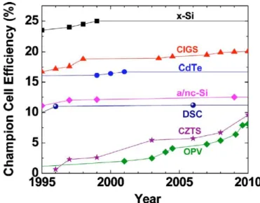
Figure 1.8 displays the champion overall power conversion efficiencies for laboratory solar cells and commercial modules for the established PV manufacturing technologies. In addition to efficiency, materials and manufacturing costs are the greatest levers controlling the cost of solar power. In most cases, the champion cells have seen little or no improvement over the past decade while economies of scale and advances in manufacturing science and technology have fueled the expansion of PV through cost reduction and module performance improvements. Figure 1.8 shows that the PV technologies are at different points in their respective learning curves when compared to the Shockley-Queisser (SQ) limit of ≈1% solar energy conversion efficiency for single junction devices (W. Shockley 1961). Since the band-gap energy dependence of the Shockley-Queisser limit is flat around the maximum, the theoretical efficiency limits for these technologies are only marginally different and are not a deciding factor in their competitiveness with each other. Nevertheless, record single crystal (c-Si) cells have matured to within 90% of their SQ limit, while commercial thin-film modules harvest about 35% of their potential.
17
Fig. 1.8. Champion efficiencies reported for cells and commercial modules for the established PV manufacturing technologies (Wolden 2011).
1.1.1. Silicon
Silicon is the most developed and well-understood semiconductor in the world, benefiting from decades of development by the integrated circuit (IC) industry. Techniques to control and manipulate its properties are well established. Silicon has proven field stability, and it is the most abundant semiconductor in the world. Multicrystalline silicon (mc-Si) remains the leading PV product, though its market share has ebbed from values as high as 65% earlier in the decade. The combination of higher efficiency, lower polysilicon prices, and improvements in wire cutting technology has reduced wafer thicknesses and kept single crystal (c-Si) silicon competitive. The issues that limit the c-Si technology today remain quite similar to those described by Goetzberger et al. in their detailed 2003 review article (A. Goetzberger 2003). The cost of the silicon feedstock remains the biggest lever impacting manufacturing costs. Reducing the cost of silicon is being pursued through a number of avenues including improving the feedstock, the production of kerfless wafers, the development of ultrathin silicon, as well as the use in bifacial cells.
18
Silicon feedstock
To date, purification techniques for silicon have been dictated by the IC industry, which employs electronic grade silicon with purity levels of less than 1 ppb. A significant shift occurred a few years ago when the PV industry surpassed the IC industry as the largest consumer of refined silicon. Electronic grade silicon is produced primarily using the energy intensive (>120 kWh/kg) Siemens process (G. del Coso 2007). New production strategies such as fluidized bed technology are being investigated, to upgrade metallurgical grade silicon, potentially reducing these energy requirements by up to a factor of 5 (Pizzini 2010). Though less expensive, these techniques often retain higher levels of metals such as Fe and Al than electronic grade silicon. While these impurities would be catastrophic in IC manufacturing, such low levels may be tolerable in solar cells.
Kerfless wafers
Improvements in wire-saw technology have enabled the reduction of wafer thicknesses to 180 /µm at present. However, over 50% of the silicon is lost as silicon sawdust or Kerf. While this material can be recycled, it would be desirable if the wire-sawing step could be eliminated. Kerfless wafer could potentially reduce Si use from an industry average of about 6-3 g/W at current wafer thicknesses. Techniques for the direct production of wafers from the melt were invented in the 1970s (Ciszek 1972) (T. F. Ciszek 1982), and after decades of development they have now reached the market. The two closely related techniques are edge-defined film-fed growth (EFG) and string ribbon silicon technologies. The elimination of wafer sawing makes this the most energy efficient mode to produce c-Si, and companies using these methods claim that energy payback times have been reduced to 1 year. The quality of the material produced by these techniques is somewhat inferior to standard block-cast mc-Si but is continuously improving with champion laboratory cells now reaching power conversion efficiencies over 18% while 4.5% efficient modules are already on the market (D. S. Kim 2006) ( Schott Solar, Albuquerque,NM, 2010). Passivation of surface and bulk defects is critical to achieving high efficiency, and this is
19
usually achieved through the deposition of a hydrogen-rich silicon nitride layer, which also serves as an antireflection coating.
Ultrathin silicon
The term ultrathin silicon (ut-Si) refers to solar cell technology where the photon absorbing silicon layer is on the order of 5-50 /μm thick. Because silicon has an indirect band gap, it is often assumed that silicon must be thicker than 100 μm to effectively absorb light (Smestad 2002). However, simulation studies have shown that ≈40 μm is ideal for obtaining maximum performance (Wolf 1980) (M. J. Kerr 2002). Green’s calculations showed that a 19.8% efficient device could be obtained with only 1 μm of single crystal silicon with state-of-the-art surface passivation (Green 1999). If one could produce such materials using a Kerfless process, it would result in an order of magnitude reduction in material cost with respect to today’s state-of-the-art wafers: thus, ut-Si would merge the benefits of crystalline silicon with those of thin-film solar cells. Thin silicon is also amenable to use of bifacial architectures, which harvest light from both directions. There are a few general approaches to the fabrication of ut-Si. The first strategy employs heteroepitaxial growth followed by liftoff or removal of a sacrificial substrate. One complication is identifying low-cost substrates with appropriate properties for these types of processes. A related approach involves deposition a-Si directly on glass followed by thermal recrystallization. The third approach involves “peeling” ultrathin silicon layers off of silicon ingots using techniques such as stress-induced liftoff (F. Dross 2007). A new process has been recently introduced where this is achieved through a combination of ion implantation and thermal treatment, producing Kerf-free wafers as thin as 25μm.
Module efficiency
While crystalline silicon solar cell science and technology is considered to be mature, there remains room to further enhance its efficiency, particularly at the module level (typical modules fall ≈20% short of record values with respect to both Voc and Jsc). Efforts to
address this include improvements in front side texturing, integration of back side reflectors, and use of advanced antireflection coatings. Another strategy is to reduce the level of shadowing associated with front contacts by either reducing the linewidths or by
20
completely eliminating them using back side contacting schemes. Another problem is that the quantum efficiency in the blue region of the spectrum is limited by high absorption and associated recombination in the vicinity of the front emitter. This issue is being addressed through the use of selective emitter designs and improved passivation strategies.
Amorphous and nanocrystalline silicon
Solar cells based on hydrogenated amorphous silicon (a-Si:H or a-Si) were first reported in 1976 (D. E. Carlson 1976). Silicon layers are deposited by plasma-enhanced chemical vapor deposition (PECVD) using mixtures of H2 and SiH4. Hot-wire chemical vapor
deposition has been offered as an alternative but has yet to be implemented in large-scale manufacturing. The addition of dopants to a-Si leads to the creation of additional recombination centers that hinder performance. Because of this effect p-i-n device structures are almost always used. Benefiting from synergies with the IC industry, a-Si was rapidly commercialized and the first PV products appeared in the early 1980s. Early devices rapidly surpassed 10% efficiency, but it was quickly recognized that these devices suffered from light-induced degradation through the now well known Staebler-Wronski effect (D. L. Staebler 1977): light exposure leads to a reduction of the solar cell efficiency over months which, eventually stabilizes at efficiencies around 6-7%. Nevertheless, for decades, a-Si was by far the most successful thin-film technology, achieving market shares approaching 10% early in the decade (A. Goetzberger 2003) before falling and being surpaszsd by CdTe a few years ago.
One of the most attractive features of a-Si is that devices can be deposited at low temperature (≤200 °C), enabling the fabrication of lightweight flexible laminates on temperature sensitive substrates. This is a unique trait that provides a competitive advantage in markets such as consumer products and building integrated photovoltaics (BIPV). Though discovered much earlier (Marecek 1968), another major change that has occurred over the past decade is the integration of microcrystalline or nanocrystalline silicon (nc-Si) into device structures. The quality of PECVD deposited material is strongly influenced by the level of silane dilution in hydrogen, and high H2 dilution levels (>90%)
21
nc-Si is that it is much less susceptible to the Staebler-Wronski degradation. Another important feature is that a/nc-Si is the only thin-film PV technology that has proven amenable to the formation of multijunction devices. Most commercial devices are based on either tandem cells or even triple junction cells. A common configuration is the "micromorph" tandem, which pairs an a-Si top cell with a nc-Si bottom cell. Solar cells with record efficiencies are based on triple junctions that employ germanium alloys to further improve absorption in the red region of the solar spectrum (J. Yang 1997). A related success story has been the introduction of the a-Si/c-Si heterojunction with intrinsic thin layer (HIT) cell, which boasts 21% conversion efficiency (M. Taguchi 2005). The intrinsic a-Si:H layers appear to be important for passivation of the underlying c-Si material.
1.1.2. CdTe
The first reports of CdTe-related PV devices appeared in the 1960s (Cusano 1963), but the development of this technology was fitful, with many stops and starts. The early 1990s saw a flurry of improvement that brought efficiencies to levels that began to attract commercial interest (J. Britt 1993). CdTe has a number of intrinsic advantages as a light absorber. First, its band gap of 1.45 eV is well positioned to harness solar radiation. Its high optical absorption coefficient allows light to be fully captured using only 2 μm of material. Like many II-VI compounds. CdTe sublimes congruently: it vaporizes homogeneously and the compound’s thermodynamic stability makes it is nearly impossible to produce anything other than stoichiometric CdTe (Cusano 1963).Thus, simple evaporation processes may be used for film deposition.
Standard CdTe-based devices employ a superstate configuration: production begins with a glass substrate followed by the successive deposition of the transparent conducting oxide (TCO, SnO2:F), the n-type window layer (CdS), the p-type CdTe absorber, and finally the
back contact (ZnTe/Cu/C). With low manufacturing costs established, the biggest opportunities for CdTe lie in the improvement of device efficiency. Champion cells (Fig. 1.8) convert just over 50% of their SQ potential, while commercial modules are at ≈11%
22
power conversion efficiency. Improving efficiency will require enhancements in both current and voltage. The former is perhaps the most straightforward route, as much of the blue region of the solar spectrum is absorbed in the TCO and CdS layers that make up the front contact. Top laboratory cells have replaced the FTO with advanced TCOs such as cadmium stannate (Wu 2004) and ITO (Compaan A. D. 2004). The more daunting challenge is improving the voltage. The open-circuit voltage (Voc) of champion CdTe cells
is below that of similar band-gap PV materials. For example, the best Voc obtained in CdTe
is 230 mV shorter of GaAs devices that have a similar band gap. Short carrier lifetimes are at the root of this limitation. The combined effect of defects and grain boundaries limits minority carrier lifetimes in polycrystalline CdTe to a few nanoseconds even in the best devices. These lifetimes are very short compared to almost 1 μs for epitaxial CdTe or hundreds of nanoseconds for copper indium gallium diselenide (CIGS). Sites and Pan (J. Sites 2007) showed through simulation that increasing the carrier lifetime or the use of a
p-i-n device structures may be two viable routes to increase the efficiency to above 20%. A
number of fundamental questions must be solved for CdTe PV to move beyond current records and approach 20% efficiency.
A final issue to be mentioned with respect to large-scale CdTe manufacturing is perceptions with respect to both cadmium toxicity and tellurium availability. The toxicity issue appears to be one of the public perceptions. Cadmium is indeed a toxic element, but the risk of exposure once incorporated into PV modules is minimal. Testing of module fate during fires, following standard protocols from the Underwriters Laboratory and the American Society of Testing Materials, showed that Cd emissions during fires are negligible as Cd is encapsulated in the glass-glass structure of the modules. Also early testing of leaking of Cd from broken CdTe modules has shown concentrations of the element in water collected over the course of a year to be below drinking water threshold (Steinberger 1998). Additional testing may be needed as module designs have changed since the 1990s. To their credit, all CdTe manufacturers are committed to 100% ownership of recycling, which in part is related to the issue of Te availability. One also notes that Cd will continue to be produced as a natural by-product of Zn mining. Perhaps the best
23
argument for CdTe PV is that it serves as a means to sequester this element in an environmentally beneficial manner.
1.1.3. CIGS
The first copper chalcopyrite PV devices were introduced in 1976 in the form of copper indium diselenide (CuInSe2 or CIS) by Kazmerski et al. (Kazmerski L. L. 1976) CIS has a
band gap of 1 eV. However, the band gap may be continuously engineered over a very broad range (1-2.5 eV) by substituting either Ga for In or S for Se. The abbreviation CIGS is now used to describe this material as current manifestations often involve either four or all five elements. Much like CdTe, the development CIGS followed a combination of starts and stops. The early 1990s brought a rapid succession of improvements that elevated device efficiencies to over 16% (L. Stolt 1993) (A. M. Gabor 1994). While most PV technologies have recorded little or no improvement in champion cell performance over the past decade, CIGS has continued a steady advance and recently-crossed the 20% threshold, making it the clear efficiency-leader among thin-film technologies (M. A. Green 2010). Substrates include soda lime glass, metal foils, or high-temperature polyimide. The latter has garnered substantial interest for applications such as BIPV and portable power. In the case of deposition on flexible substrates it is critical to match the coefficient of thermal expansion, with highest efficiencies obtained on titanium and stainless steel foils. The insulating nature of PI is advantageous for monolithic integration, but process temperatures are limited to <450 ° C, which limits efficiency.
The basic structure of the CIGS device is quite similar across manufacturers. Fabrication begins with the deposition of a Mo back contact followed by the p-type CIGS absorber (1-3 µm), a thin buffer layer (50>100 nm), with doped ZnO serving as the transparent front contact. Here the similarities end.The approaches to CIGS fabrication may be classified into three basic categories: coevaporation, selenization/sulfurization of metal films, and nonvacuum techniques (M. A. Contreras 1999) (K. Ramanathan 2005) (C. J. Hibberd 2010).
24
The nonvacuum strategies may be further divided into electrodeposition, particulate deposition, and solution processes. Electrodeposition has been around for decades and achieved cell efficiencies as high as 13.8% (Lincot et al. 2004), but concerns about up-scaling have limited commercial interest. The particulate route is currently the most actively pursued, with variations employing particles composed of CIGS, metal, metal oxides, and/or metal selenides.
Material chemistry
With five elements and numerous binary and ternary phases, the CIGS system presents much greater complexity than the PV technologies described previously. Extensive theoretical work has made great advances in understanding the electronic structure and role of defects in this system. These studies have been aided by improvements in advanced characterization techniques. Raman and time resolved photo-luminescence are becoming useful for identifying the presence of secondary phases and certain defects (M. A. Contreras 1999). It is well known that sodium plays a critical role in the morphology and electronic properties of CIGS. Some concerns remain about the use of ZnO as the front TCO and its potential impact on long-term device stability. Moisture exposure is particularly detrimental both to the TCO and the heterojunction itself. Encapsulation in glass partially alleviates this effect, but further development of transparent ultrabarriers is required to improve the long-term stability of flexible CIGS solar cells. (G. L. Graff 2004). A longer-term concern is the availability and price of In. Recycling of this metal will alleviate constraints on CIGS long-term production, but research is needed to develop technologies for efficient and low-cost recycling of all the elements from the CIGS modules. The possibility of substituting indium/gallium with earth abundant alternatives such as zinc/ tin is discussed below.
1.1.4. Organic photovoltaics
Carbon is abundant, and the potential for high volume manufacturing of flexible photovoltaics has spurred extensive efforts to develop solar cells using organic semiconductors. Figure 1.9 charts the progress of champion cell efficiencies for the past 15
25
years. While most technologies have been relatively stagnant in their champion efficiency, organic PV has made great strides in the past decade, with Heliatek and Konarka being the current champions, each with devices certified at 8.3% (Heliatek 2010) (Konarka 2010). OPV devices are comprised of a heterojunction between an electron donor molecule (e.g., poly(3-hexylthiophene) or copper phthalocyanine) and an electron acceptor molecule (e.g., C60 or its derivatives such as phenyl-C61-butyric acid methyl ester). The essentially limitless varieties of candidate organic semiconductor materials may be categorized, as either solution processable (polymers, dendrimers, oligomers, or small molecules) or vacuum deposited (small molecules or oligomers). Although superficially similar to inorganic p-n junctions, the OPV junction is fundamentally different. Instead of directly creating an e-/h+ pair, photon absorption produces an exciton, an uncharged excited state that must diffuse to a donor/acceptor interface in order to dissociate into a free e-/h+ pair.
In organic materials the exciton can typically diffuse only 5-10 nm before decaying to the ground state, a problem that limits performance and is typically referred to as the exciton bottleneck. There are two ways to deal with this. One can make a multilayer device that uses very thin donor/acceptor layers such that a majority of excitons can diffuse to a heterojunction interface. Otherwise, one can reduce the distance the exciton has to diffuse before reaching the heterojunction by mixing the donor and acceptor materials on a nanometer length scales to form a single-layer interpenetrating network called a bulk heterojunction. This approach is commonly used in solution-processable materials.
In the OPV device structure, the heterojunction active layer(s) is (are) sandwiched between a set of contact electrodes, with buffer layers likely to be present. In the bulk heterojunction approach an asymmetry in the device must be imposed by either using electrodes with different work functions (typically a front TCO contact modified with a conducting polymer poly(3,4-ethylenedioxythiophene) poly-(styrenesulfonate) and a back contact metal of Ca or Al) or by inserting a buffer layer that blocks carriers from leaving one side of the device. An oxide buffer layer is commonly inserted to block holes from leaving the device through the front TCO contact, which inverts the direction of operation of the device and allows the use of a high work function Ag back contact. In the vacuum
26
deposited multilayer approach, co-doping of buffer layers has been used to great effect to produce a true p-i-n structure that obviates the need for a mismatch in the contact work functions.
Fig 1.9. Evolution of champion cell efficiencies since 1995 for various PV technologies (Wolden e al. 2011).
There are several challenges to improve the efficiency of organic solar cells (Brabec C. J. 2010) (H. Spanggaard 2004). These are being addressed through the development of novel donor and acceptor materials, new buffer layers, and electrode geometries, innovative processing, and through the use of tandem architectures. A key issue is to significantly raise the short circuit current density (JSC) to above 20 mA/cm2. Present values are
typically 10-12 mA/cm2 with champion values approaching 17 mA/cm2 (C. J. Brabec 2010). Advanced photon management strategies are also being pursued to increase optical absorption. A second challenge is to increase the open-circuit voltage. Key to this is achieving optimal band alignment of the device structure and minimizing the band offset between donor and acceptor molecules while maintaining efficient charge transfer. Third, the fill factors (FF) have to be increased beyond 0.7, which has been achieved in only a
27
few champion devices.Organic solar cells typically have poor FF relative to conventional
p-n junctions. This is due to high series resistance and/or carrier recombination, as the
carrier mobility in organic thin-films is lower than their inorganic counterparts. Simultaneous achievement of JSC=20 mA/cm2, VOC =0.8 V, and FF=0,7, leading to an
efficiency of 11%, has not been achieved yet. Doing this in a single junction device will require simultaneous optimization of all the materials and interfaces. With existing materials and devices, the energy payback time for OPV has been estimated to be between 0.3 and 3 years. This relatively high level of uncertainty reflects the range of assumptions used for this still developing technology. However, an efficiency of closer to 15% may be needed to achieve a true grid-parity leveled cost of electricity of ~$0.07/kW h. Much work still needs to be done to demonstrate acceptable performance in large area modules.
Another important issue that has to be resolved is the stability of organic solar cells. The chemical, physical, and mechanical degradations that are predominant in OPV materials and devices have been well discussed (M. Jørgensen 2008). The current goal is to increase lifetimes from 3 to 5 years, which is expected to be sufficient for consumer applications. Due to the flexibility of organic synthesis, it can be estimated that there are on the order of 1013 different material combinations that could be employed. Whether the right combination of properties (e.g., band gap, charge mobility, exciton diffusion length, etc.) exists and how to identify them remain open questions.
1.1.5. Dye-sensitized solar cells
Dye-sensitized solar cells are based on the photoelectro-chemical effect discovered by Bequerel in 1839. A relatively new concept, DSSC, was introduced by O’Regan and Gratzel in 1991. (B. O’Regan 1991). They proposed a device based on a hybrid material typically composed of organometallic dye molecules adsorbed on a mesoporous wide band-gap semiconductor and an electrolyte filling the pores. The dye provides high absorption in visible range, thus enabling efficient conversion of sunlight; the working mechanism of DSSC will be discussed in detail in the next chapter. Dye sensitization of oxides was well known at that time, and Gratzel’s key innovations were in creating a
28
nanoparticles film with high surface area to improve light harvesting and in choosing components with appropriate kinetics for fast charge transfer and slow recombination. Gratzel’s group rapidly optimized the device to over 10% within a few years of its introduction (M. K. Nazeeruddin 1993). This brought the attention of industry and today a number of small companies are engaged. Most current products are directed at the consumer market, for example, DSSC on flexible substrates that replace rechargeable batteries for portable electronics. A beneficial feature of DSSC is that their performance improves under diffuse and low light conditions (Tulloch 2004), enabling their use indoors and without direct solar exposure. Devices can be fabricated in a number of colors and levels of transparency, which is an attractive feature for architectural and architectural applications. Recent trends evolve to the Building Integrated PhotoVoltaics (BIPV) to replace conventional building materials in parts of the building envelope such as the roof, skylights or facades (F. -T. Kong 2007). According to how and where such systems are built, whether into the facade or in the roof, the BIPV systems are different (Luque A., Handbook of Photovoltaic Science and Engineering 2003). In the case of facade or roof systems the photovoltaic modules are added to the building after it is built. These low powered systems of up to some 10 kW are usually integrated into the south facade. Facade integrated photovoltaic systems could consist of different transparent module types. In such case a part of natural light is transferred into the building through the modules. Solar cells are available in different colours; therefore, there is no limitation for imagination of the architect or the designer. Such constructed buildings give the term architecture a completely new meaning.
Roof-integrated photovoltaic systems are integrated into the roof, that is covered with photovoltaic modules. It is possible to use tiles that integrate solar cells. Photovoltaic systems could be used for shadowing, where photovoltaic modules serve as venetian blinders. In some of such cases photovoltaic modules tilt angle could be adjusted manually or automatically allowing for shadowing the building and/or photovoltaic module efficiency optimization. Such systems are also known as “Shadow-Voltaic” systems. Even if the area-related investment costs of a PV building element is higher than the cost of
29
conventional high-end elements, the electricity generated and the benefit of architectural double uses may compensate for this difference within a reasonable time (Tulloch 2004). Manufacturing can also be done at low temperature using flexible substrates.
Unfortunately, the champion cell efficiency has been stagnant at ~11% for the past 15 years (Fig. 1.9). Higher efficiency values have been reported for small-area cells. In 2006, Chiba et al. achieved an AIST-validated efficiency of 11.1% using the so-called black dye, a ruthenium terpyridyl complex (coadsorbed with deoxycholic acid) and a masked area of 0.219 cm2. More recently, slightly higher efficiencies (up to 12.1%) have been reported for small-area (0.28 cm2) DSSC utilizing hexyl(thiophene)-conjugated bipyridine ligands. With respect to manufacturing numerous module fabrication strategies are being pursued, which, in general, can be divided into monolithic or sandwich constructions. The former offers advantages with respect to material cost, while the latter may be more amenable to roll-to-roll processing. Substrates include glass, metal, and polymer foils, with best performance being obtained on glass. Critical issues include stability and the production of large area modules. At present minimodules with areas <100 cm2 are used, with resistance losses being one of the major problems. The stability of a DSSC module is strongly related to the device encapsulation. Standard practices for lifetime and stability testing do not exist for DSSC. However, long-term light soaking at 55-60 °C under resistive load has shown that efficiencies remain above 80% of their initial value for over 25 000 h (Desilvestro 2011 ). These Dyesol data on ~ 1 cm2 cell indicate that carefully encapsulated glass-based DSSC can last for over 20 years in a typical Middle European climate. The longest outdoor test of DSSC modules (110 cm2) by Toyota and Asin was 2.5 years, showing efficiency losses of 6% (relative) per year (N. Kato 2011). Faster degradation could be attributed to differences related to sealing methods, cell/module area, or environment. Hermetically sealing flexible DSSC is more challenging, and current products using DSSC on plastic substrates have lifetimes of only a few years. For outdoor applications, the sealing material must, for example, be mechanically and thermally stable, stable under UV exposure, and chemically inert to the electrolyte. Moreover, it should prevent mass transport between adjacent cells. The issue is so important that Hagfeldt et al. (A. Hagfeldt 2010) suggested
30
that the leading manufacturing approach for DSSC may be the one that provides the most functional encapsulation method. Replacing the liquid electrolyte with a gel or solid would greatly reduce encapsulation requirements, but these changes have resulted in decreased efficiency. Elimination of glass, implementation of roll-to-roll manufacturing methods, and increased lifetimes will be critical to economics particularly if device efficiency remains below 12%.
It is interesting to compare these “champion” efficiencies with those of competing thin-film technologies. All of these values are for cells that are 1 cm2
in area. The most remarkable of these values is the 8.3% for organic cells, which are threatening to catch-up with DSSC. Clearly, competition is strong, and if the DSSC technology is to evolve into a mature and successful commercial one, the current efficiency bottleneck needs to be addressed.
The three main components in a DSSC, the Ru-based dye, the photoanode, and the iodine-based redox couple, have remained largely unchanged. Further optimization of any one of these components individually is not likely to yield significant improvements in efficiency. The recent review by Hamann et al. (T. W. Hamann 2008)provides an excellent overview of the complexity of the issues involved. First, the leading dye does not capture much light past 750 nm, and harvesting the red and near-infrared portions of the spectrum is needed to increase current densities. In addition, replacing Ru is an important long-term concern with respect to material availability. Second, the I3-/I- redox couple is positioned with a 550 mV
overpotential relative to dye regeneration. An alternative redox couple could potentially allow the Voc to be improved by up to 300 mV, but recombination rates are typically much
faster with non-iodine redox couples. A combination of these two changes could elevate device performance to >16%. However, as cautioned by Hamann et al. (T. W. Hamann 2008), this will most likely require simultaneous optimization of both dye and electrolyte and perhaps the development of new photoanodes with faster charge transport as well. Photoanode designs based on wide band gap semiconductor nanowires have been applied
31
to improve efficiency, but six years after their first introduction, their performance remains low.
1.5.MATERIAL AVAILABILITY AT TW/YR MANUFACTURING
Manufacturing solar cells at a rate of 1 TW/yr will be a colossal undertaking, and will be strongly conditioned by the availability of material resources. The two elements of concern most often discussed are tellurium and indium (Andersson 2000) (Green 2009). The former is a by-product of copper mining, while indium is a by-product of zinc extraction. Tellurium is one of the least abundant elements in the earth’s crust, comparable to the platinum group metals. However, there is great debate and uncertainty in the assessments of Te resources, with the level of concern ranging from critical to manageable to nonexistent. Indium is also scarce, and there are concerns about its price and preferred use in higher value products such as flat panel displays. One concern is that rising demand will increase prices of indium and tellurium by several factors so that the absorber material will become more expensive and larger fraction of the material cost. Such a rise can quickly erode the cost advantages of CdTe and CIGS thin-film technologies.
1.6.FUTURE OUTLOOK
Redefining the boundaries of PV technologies
Photovoltaic technologies are often classified as being either first generation (c-Si), second generation (thin film), or third generation concepts that have the potential to overcome the SQ limit such as devices that employ multijunctions, extract hot carriers, or involve multiple electron/exciton generation (Green 2001). In 2001, Green formally classified the potential of first, second, and third generation technologies with respect to both power conversion efficiency and manufacturing costs, and his diagram is reproduced in Fig. 1.10. The quotient of these two variables is proportional to the cost/Wp, which is reflected by the
32
generations provided by Green. Advocates of DSSC and OPV often describe these platforms as third generation concepts. However, it should be noted that Green did not make this distinction, limiting his definition to those concepts that can exceed the SQ limit. In practical terms DSSC and OPV should be considered thin-film technologies, ideally competing for the low-cost region of oval II in Fig. 1.10.
Fig. 1.10. Green’s 2001 classification of PV technologies superimposed with the current status (solid and projected evolution) (Wolden 2011).
One of the key points that came out of the workshop discussions was the idea that these accepted boundaries have become outdated. It has become clear that CdTe and c-Si are not bound by the limits imposed by Green’s original figure. The current status and projected future of these two technologies have been added to Fig. 1.10. The point for CdTe reflects the present status of First Solar’s technology, which is based on 11.2% modules and self-reported production costs of $0.77/Wp, putting it on the fringe of the second generation
domain. The arrow indicates the expected potential of this technology based on the discussions above. Through improvements in efficiency and further integration of manufacturing it is not unreasonable to expect CdTe manufacturing costs to drop below $0.5 /Wp within the next decade.
33
The diversity of products makes the situation for c-Si more complex to analyze, but the revised oval for c-Si also sits on the edge of the initial bounds proposed by Green. Module efficiencies range from 15% to 22%, with leading production costs as low as $1.10/Wp
reported by Trina Solar in the second quarter of 2010. Again, the arrow leaving the oval represents the future potential of this technology as discussed above. Here, the largest gains are related to further reduction in the production costs through reduction in Si requirements, as well as boosting module efficiency closer to 25%. This combination provides a pathway that approaches $0.5/Wp. Some may find this projection overly
optimistic. However, one of the enlightening consequences of First Solar’s emergence has been the ability of the c-Si industry to rapidly respond and reduce its costs. It is also important to note that silicon does not have to move as far as CdTe. As module costs drop below $l/Wp they become increasingly less important as balance of system issues including
inverters, racks, installation, and space become important cost drivers. These costs drop with module efficiency, and thus silicon can afford to remain competitive despite higher manufacturing costs than CdTe. It is too early to project what may happen to CIGS, though it is plausible to expect that it might end up in a similar region, most likely somewhere between CdTe and c-Si.
34
Chapter 2. Dye sensitized solar cells
This chapter introduce dye-sensitized solar cells technology: from the working principle to the materials in use. Advantages and drawbacks related to this class of device are put in evidence to introduce the results presented in the following chapters.2.1 STRUCTURE AND WORKING PRINCIPLE
A dye-sensitized solar cell can be considered as a hybrid of photogalvanic cells and solar cells based on semiconductor electrodes (K. Kalyanasundaram 1998). It consists of a dye-coated semiconductor electrode and a counter electrode arranged in a sandwich configuration, the inter-electrode space being filled with an electrolyte containing a redox mediator (Fig. 2.1).
35
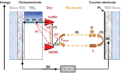
Under light irradiation, the dye molecule are photo-excited, and in time of the order of femtoseconds injects an electron into the conduction band of the semiconductor electrode; the original state of the dye is subsequently restored by electron donation from the electrolyte, usually an organic or ionic liquid solvent containing the I3-/I- redox system (F.
-T. Kong 2007), (A. Luque 2003). The iodide is regenerated, in turn, by reduction of triiodide at the counter electrode, the circuit being completed through the external load. The voltage generated under illumination corresponds to the difference between the Fermi level of the electron in the semiconductor electrode and the redox potential of the electrolyte. Overall, electric power is generated without permanent chemical transformation. These primary processes can be schematically summarized (see Fig. 2.2) by the following reactions (A. Luque 2003) (J. Halme 2010).
Fig. 2.2: Operating principle of a DSSC (J. Halme 2010). The black and red arrows show the forward and back reactions, respectively.
36
1) The photosensitizers (typically Ru complex) adsorbed on the porous semiconductor material surface (TiO2) absorb incident photon flux. The photosensitizer is excited from
the ground state S to the excited state S* due to the metal-ligand charge transfer transition. S + hν → S* - light absorption by the dye -
2) The excited electrons are injected into the conduction band of the TiO2 electrode,
resulting in the oxidation of the photosensitizer. S*→S+
+ e- (TiO2) - electron injection-
3) The oxidized photosensitizer S+ accepts one electron from the I- ion redox mediator, regenerating the ground state S, while I- is oxidized to I3-.
2S+ + 3I-(PA) → 2S+I3- (PA) -dye regeneration-
4) Injected electrons in the conduction band of TiO2 are transported in TiO2 toward the
front contact (TCO) and consequently reach the counter electrode through the external load and wiring.
e-(TiO2) →e-(PA) -electron transport
At the counter electrode (CE):
5) The oxidized redox mediator I3- diffuses toward the counter electrode and is again
reduced to I- ion (the electrons are returned to the cell)
I3-(CE) + 2e-(CE) → 3I-(CE) -overall charge transfer reaction-
At the electrolyte:
6) The electrical circuit of the cell is completed by ionic transport of the redox pair in the electrolyte,
3I-(CE) → 3I-(PA) -iodide diffusion- I3-(PA) →I3-(CE) -tri-iodide diffusion-
The total reaction is given by:
3I-(PA) + 2hν →I3-(PA) + 2e-(TiO2) -photoanode
e- (CE) + hν → e-(PA) -cell-
The back reactions limiting the photocurrent (fig. 2.2) are: a) the non radiative relaxation of the excited state of the dye b) the recombination of the electrons with the oxidized dye
37
c) the recombination of the electrons with the tri-iodide in the electrolyte.
The performance of a DSSC is predominantly based on four energy levels of the components (A. Luque 2003): the excited state (approximately LUMO-Lowest Unoccupied Molecular Orbital) and the ground state (HOMO-Highest Occupied Molecular Orbital) of the photosensitizer, the Fermi level of the TiO2 electrode, which is located near
the conduction-band level, and the redox potential of the mediator (I-/I3-) in the electrolyte
(Fig.2.3).
Fig. 2.3: Schematic energy diagram of a DSSC (A. Luque 2003).
The photocurrent obtained from a DSSC is largely determined by the energy difference between the HOMO and the LUMO of the photosensitizer, analogously to the band gap, Eg, for inorganic semiconductor materials. The smaller the HOMO-LUMO energy gap, the
38
the solar spectrum. The energy gap between the LUMO level and the conduction-band level of TiO2, ΔE1, is important, and the energy level of the LUMO must be sufficiently
negative with respect to the conduction band of TiO2 to inject electrons effectively. In
addition, substantial electronic coupling between the LUMO and the conduction band of TiO2 also leads to effective electron injection. The HOMO level of the complex must be
sufficiently more positive than the redox potential of the I-/I3-- redox mediator to accept
electrons effectively (ΔE2). The energy gaps, ΔE1 and ΔE2, must be larger than
approximately 200 mV as driving force for each of the electron-transfer reactions to take place with optimal efficiency.
The voltage in the DSSC is developed by the energy gap between the Fermi level of a TiO2
electrode and the redox potential of the I-/I3- in the electrolyte. The conduction-band level
of the TiO2 electrode and the redox potential of I-/I3- were estimated to be respectively -0.5
V and 0.4 V versus normal hydrogen electrode (NHE). Thus the maximum voltage is expected to be approximately 0.9 V, because the Fermi level of the TiO2 electrode depends
on the electrolyte components and their concentrations.
In contrast to a conventional p-n type solar cell, the mechanism of a DSSC does not involve a charge-recombination process between electrons and holes, because electrons are only injected from the photosensitizer into the semiconductor and a hole is not formed in the valence band of the semiconductor. In addition, charge transport takes place in the TiO2
film, that is separated from the photon absorption site (i.e. the photosensitizer); thus, effective charge separation is expected. The photon-to-current conversion mechanism in a DSSC is similar to the mechanism for photosynthesis in nature, in which chlorophyll functions as the photosensitizer and charge transport occurs in the membrane.
In conventional p-n type solar cells and classical solar cells using polycrystalline or single crystal photoelectrodes, the establishment of equilibrium between the Fermi level of the materials from the photovoltaic junction leads to space charge formation. Photogenerated charges are separated by the electric field in the space charge layer. In DSSC, however, the individual particle size is too small to form a space charge layer. Charge separation in DSSC has been discussed relative to an electrical field at the electrolyte/semiconductor
39
interface (A. Zaban 1998). Small cations, such as Li+, in the electrolyte and H+ released from the dyes upon binding, can adsorb (or intercalate) on the semiconductor surface (A. Luque, Handbook of Photovoltaic Science and Engineering 2003). A dipole is formed across the Helmholtz layer between these cations and negatively charged species (iodide ions and the dye). The electrical potential drop across the Helmholtz layer can help to separate the charges and reduce recombination with the dye cations or the redox mediator. Under illumination, this potential will decrease, as the electrons injected in the semiconductor will neutralize some of the positive charge at the surface.
2.1. DSSC MATERIALS
The basic structure of a DSSC presented above is based upon some important materials: the TCO (Transparent Conductive Oxide)-glass substrate, the TiO2, the dye sensitizer, the
electrolyte and the counter electrode.
2.1.1. TCO-conductive glass substrate
The TCO-coated glass is used as the substrate for the electrodes (A. Luque, Handbook of Photovoltaic Science and Engineering 2003). For high solar cell performance, the substrate must have low sheet resistance and high transparency. In addition, the material should be heat resistant up to 500 °C because this temperature is reached during the standard cell fabrication process.
Indium–Tin oxide (ITO) is one of the most famous TCO materials. In spite of having low resistance at room temperature, ITO resistance increases significantly after high temperature treatment in air. Therefore, the more stable fluorine-doped SnO2 (FTO) is used
40
2.1.2. TiO2 semiconductor electrode
Photoelectrodes made of common semiconductors as Si, GaAs, InP, and CdS decompose under irradiation in solution owing to photocorrosion. In contrast, oxide semiconductor materials have good chemical stability under visible irradiation in solution. Semiconductor oxides used in dye-sensitized solar cell include TiO2, ZnO, SnO2, Nb2O5, and so forth,
which serve as the carrier for the monolayers of the sensitizer using their huge surface and the medium of electron transfer to the conducting substrate(F. -T. Kong 2007) . So far, TiO2 is the best choice in semiconductor due to low price, abundance in the market,
nontoxicity, and biocompatiblity, (it is also used widely in health care products as well as in paints). DSSC photoanodes will be extensively discussed in chapter 5.
2.1.3. Dye photo-sensitizer
Dye sensitizers serve as solar energy absorber in DSSC, whose proprieties have much effect on the light harvesting efficiency and the overall photoelectric conversion efficiency (F. -T. Kong 2007). The ideal sensitizer for dye-sensitized solar cells should absorb all light below a threshold wavelength of about 920 nm. In addition, it should be firmly grafted to the semiconductor oxide surface and inject electrons to the conduction band with a quantum yield of unity. Its redox potential should be sufficiently high that it can be regenerated rapidly via electron donation from the electrolyte or a hole conductor. Finally, it should be stable enough to sustain at least 108 redox turnovers under illumination, corresponding to about 20 years of exposure to natural light. The best photovoltaic performance in terms of both conversion yield and long-term stability has been so far achieved with polypyridyl complexes of ruthenium and osmium. The sensitizers used in DSSC are divided into two types: organic dyes and inorganic dyes, according to their structure. Inorganic dyes include metal complexes, such as polypyridyl complexes of ruthenium and osmium, metal porphyrin, phthalocyanine and inorganic quantum dots, while organic dyes include natural organic dyes and synthetical organic dyes.
Compared with organic dyes, inorganic complexes dyes have higher thermal stability and chemical stability.
41
Among these complexes, polypyridyl ruthenium sensitizers were widely used and investigated for their high stability and outstanding redox properties and good response to natural visible sunlight. The sensitizers are anchored on the surface of the semiconductor electrode with carboxylate groups or phosphonate groups, that enable the electron injection into the conduction band of the semiconductor. Polypyridyl ruthenium dyes may be divided into carboxylate polypyridyl ruthenium dyes, phosphonate ruthenium dyes, and polynuclear bipyridyl ruthenium dyes. The difference between the first two types of sensitizers lies in the adsorption group. The first two types of sensitizers differ from the last type of sensitizer in the number of metal centres. The carboxylate polypyridyl ruthenium dye is in level structure, which enables the electron injection into the conduction band of the semiconductor quantitatively. Among these sensitizers, N3 and its tetrabutylammonium salt N719, black dye (fig. 2.9, 2.10) showed unmatched performance.
Fig.2.4.Molecular structure of the most used dyes.
Carboxylate polypyridyl ruthenium sensitizers are easily desorbed from the surface in aqueous solution when the pH value is lower than 5, though they have a lot of advantages. The phosphonate polypyridyl ruthenium sensitizers use phosphonate group to be anchored to the surface of the semiconductor, that is hardly desorbed from the semiconductor surface