UNIVERSITA' DEGLI STUDI di MESSINA
DI: DIPARTIMENTO DI INGEGNERIA
PhD in Engineering and Chemistry of Materials and Construction
Multi-Level Inverters exploiting an Open-end
Winding configuration
Salvatore Foti
PhD Coordinator: Prof. S. Galvagno
Tutor: Prof. A. Testa
1
Acknowledgments
First, I would like to express deep appreciation to my supervisors: Prof. A. Testa, Prof. G. Scelba, Prof. S. De. Caro and Prof. G. Scarcella, this research report has been developed thanks to their guidance and valuable advices.
Secondly, I would like to thank the Department of Engineering of the University of Messina, the Department of Electrical and Electronic Engineering and Computer Science of the University of Catania and the “CePTIT” center, where, during the last three years, I have studied, talked and realized many things together with other colleagues and students.
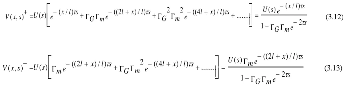
In particular, I would like to acknowledge: Angelo Sciacca, Dario Bazzano, Mario Pulvirenti, Daniele Caruso, Gianni Nobile, Tommaso Scimone and Luca Finocchiaro.
I would like to thank my parents, my brother and my girlfriend Elisa for being such a huge support through my experiences! I could not have made it without you all!
Last but not least, I need to thank all people that I am forgetting now!
Salvatore Foti January 2017
2
Table of Contents
Acknowledgments ………..………..……… 1
Table of Contents ... 2
Introduction... 4
1 Chapter: State of the Art of Multilevel Converters ... 6
1.1 Standard Multilevel inverter topologies ... 6
1.1.1 Neutral Point Clamped Inverter ... 10
1.1.2 Flying Capacitor Inverter ... 12
1.1.3 Cascaded H-Bridge Inverters... 15
1.1.4 Recent advances in MLI topologies ... 16
1.1.5 Control and Modulation Strategy for MLIs ... 20
1.2 References of Chapter 1 ... 27
2 Chapter: Open-end Winding Systems ... 33
2.1 Definition and features of an Open-end Winding System... 33
2.1.1 Symmetrical Dual Two-level Inverter with single DC-Bus ... 38
2.1.2 Symmetrical Dual Two-Level Inverter with two isolated DC-Buses ... 40
2.1.3 Asymmetrical Dual Two-level Inverter with two isolated DC-Buses ... 43
2.1.4 Review on Common-Mode Voltage and Zero Sequence Current in a Dual Two-Level inverter fed an Open-end Winding machine ... 44
2.2 References of Chapter 2 ... 55
3 Chapter: Overvoltage Phenomena in AC Motor Drives ... 59
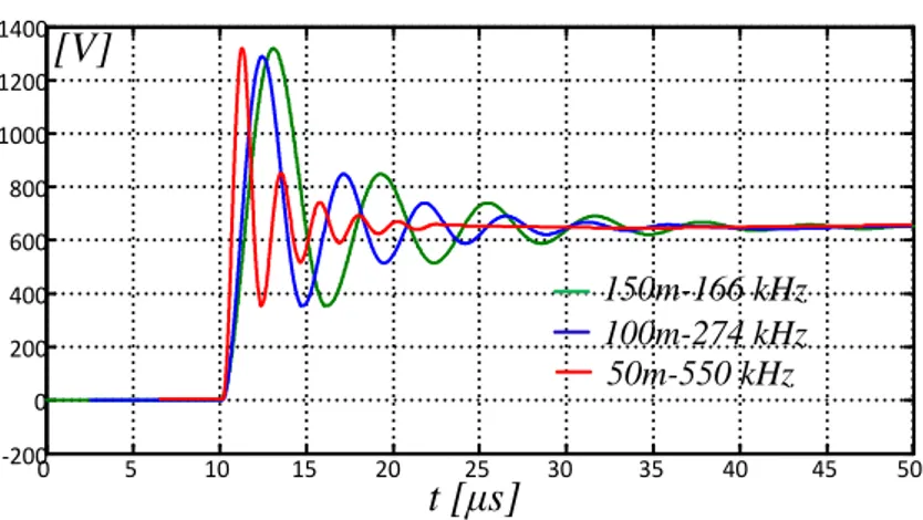
3.1 Study and presentation of the problem ... 59
3.1.1 Transmission Line Theory and Factors affecting the Overvoltage ... 61
3.1.2 Motor overvoltages < 2 DC Bus voltage ... 66
3.1.3 Motor overvoltages > 2 DC Bus voltage ... 67
3.1.4 Overvoltage Mitigation Techniques based on additional passive networks ... 70
3.1.5 Active Overvoltage Mitigation Techniques ... 82
3.2 Proposed overvoltage mitigation on Open-end Winding AC Motor Drive ... 88
3.2.1 Dwell Time impact on Inverter output voltage... 93
3.2.2 Dwell Time Adaptation ... 95
3.2.3 Experimental Validation ... 96
3.2.4 Proposed RC Passive Filter on Open-end Winding AC Motor Drive ... 98
3.3 References of Chapter 3 ... 100
4 Chapter: Asymmetrical Hybrid Multi-Level Inverter (AHMLI) ... 103
3
4.1.1 Space vector combinations of AHMLI ... 105
4.1.2 Low-frequency modulation in MLI ... 108
4.1.3 Active harmonic elimination method ... 111
4.1.4 Simulation results of the harmonic suppression method: THD and Power Losses ... 113
4.1.5 Experimental results on AHMLI AC Motor Drives: V/f control ... 121
4.1.6 AHMLI Motor Drive Efficiency ... 127
4.2 Field Oriented Control on AHMLI AC Motor Drives ... 129
4.2.1 Simulation and Experimental results on AHMLI AC Motor Drives ... 132
4.3 AHMLI approach for STATCOM and Generators ... 134
4.3.1 AHMLI current control system for STATCOM and Generators ... 138
4.3.2 AHMLI current control system with grid current harmonic compensation ... 142
4.3.3 AHMLI Conversion Efficiency for STATCOM and Generators ... 150
4.4 AHMLI for High-Speed Gen-Set Applications ... 151
4.5 References of Chapter 4 ... 161
5 Multi-Motor Drive Exploiting the AHMLI approach ... 164
5.1 Proposed Open-end Winding Multi-Motor Drives (OW MMDs) ... 167
5.1.1 Open-end Winding Multi-Motor Single Converter ... 168
5.1.2 Open-end Winding Multi-Motor Multiple Converters ... 178
5.2 References of Chapter 5 ... 188
4
Introduction
Multilevel converters are becoming more and more popular, overcoming some key limitations of conventional two-level structures in handling medium voltages and high voltage gradients. Today they provide the ground for the realization of high efficiency energy conversion systems for medium voltage applications, such as pumps, compressors, extruders, fans, grinding mills, rolling mills, conveyors, crushers, blast furnace blowers, gas turbine starters, mixers, mine hoists, reactive power compensation, marine propulsion, wind energy conversion, and railway traction. A detailed overview of multilevel converters is provided in Chapter 1, while, the state of the art of Open-end Winding Systems is described in Chapter 2. The last systems can be considered as special multilevel inverter structures, tailored around an electrical machine fed from both the ends of the stator, or primary, winding. Overvoltage phenomena generated in industrial motor drives at motor terminals by long feeding cables are investigated in Chapter 3 and an Open-end Winding configuration approach is presented to actively mitigate them. Moreover, an adaptive algorithm is described to make independent the active overvoltage mitigation from system parameters. The main contribution of this work is the development of a new multilevel inverter topology, the Asymmetrical Hybrid Multilevel Inverter (AHMLI), which is introduced in Chapter 4. According to the AHMLI structure, an open end winding machine (motor, generator or transformer) is supplied on one end by a main multilevel converter, fully managing the active power stream, and, on the other end by an auxiliary two level inverter. This acts as an active power filter, suitably shaping the electrical machine phase current. A mathematical analysis of the proposed structure is first provided, followed by an exhaustive comparison between AHMLI and conventional multilevel structures, emphasizing advantages in terms of efficiency and output current THD. Voltage and current control systems, optimally coping with key characteristics of the AHMLI structure are carried out and an original input capacitors voltage equalization technique is also presented. The application of the AHMLI concept to industrial induction motor drives is then evaluated by simulation and experimental test. A possible exploitation of the AHMLI approach in the realization of photovoltaic and wind plants, as well as STATCOM devices is also assessed. Moreover, a high efficiency three phase rectifier for high speed generation systems exploiting the AHMLI configuration is carried out. Finally, the application of the AHMLI approach to Multiple Motor Drive systems is proposed in Chapter 5. Two new topologies are presented, namely: Open-end Winding Multi Motor Single Converter (MMSC) and Open-end Winding Multi Motor Multi Converter (MMMC). Both configurations exploit the
5
AHMLI structure but the MMMC exploits a five-leg two level inverter to independently control the stator currents of two induction motors.6
1 Chapter: State of the Art of Multilevel
Converters
Multilevel converters are today successfully exploited in many industrial applications such as pumps, compressors, extruders, fans, grinding mills, rolling mills, conveyors, crushers, blast furnace blowers, gas turbine starters, mixers, mine hoists, reactive power compensation, marine propulsion, high-voltage direct-current (HVDC) transmission, hydro pumped storage, wind energy conversion, and railway traction [1]-[10]. However, such a technology is still under development, and many new contributions and new circuital topologies have been proposed in the last few years. Many publications of tutorial nature have recently addressed the multilevel converter technology, emphasizing the growing importance of multilevel converters for high-power applications [4]-[9]. These works cover in depth traditional and well-established multilevel converter topologies, such as the neutral point clamped (NPC), cascaded H-bridge (CHB), and flying capacitor (FC), as well as specific modulation strategies. The most attractive features of multilevel inverters, over conventional two-level inverters, are:
MLIs can generate output voltages with low distortion in term of Total Harmonic Distortion THDv;
MLIs draw input current with very low distortion in term of THDi;
MLIs generate output voltages with lower dv/dt, thus reducing the voltage stress across power devices and at the same time mitigating overvoltages at the load terminals;
MLIs generate smaller common-mode voltage CMVs, thus reducing the bearing currents. Additional modulation methods can be adopted in order to eliminate the CMVs;
MLIs can operate with a lower switching frequency.
In this chapter an overview of classic multilevel topologies is presented, together with the latest developments of multilevel modulation strategies. A particular attention is also played to multilevel converter control and operational issues, such as harmonic elimination and DC Bus capacitors voltage balancing.
1.1 Standard Multilevel inverter topologies
The development of the multilevel converter technology was started in the late 1960s with the introduction of a series-connected H-bridge converter with a multilevel stepped waveform voltage modulation, which became the H-Bridge converter (CHB) topology [11]. This was closely followed by low-power development of a Flying Capacitor (FC) converter topology [12]. In the late 1970s, the Diode-Clamped Converter (DCC)
7
[13] has been first introduced, that is today known as Neutral Point Clamped (NPC) inverter. This last has been proposed in [14], [15] and it can be considered as the first real multilevel power converter for medium-voltage applications. In the late 1980s [16], the CHB has been reintroduced although it reached more industrial relevance in the mid-1990s [17]. In the same way, in the early 1990s, the original low power FC converter evolved to the medium-voltage multilevel converter topology we know today [18]. Through the years, the FC has also been reported as the imbricated-cell and multi-cell converter. CHB, NPC and FC multilevel converters are considered now as the classic or traditional multilevel topologies and their development turned out in industrial products during the last two decades, Fig. 1. 1. These converters are today produced by several firms [19]–[34], offering different power ratings, front-end configurations, cooling systems, semiconductor devices, and control schemes. The most relevant parameters and ratings for each classic topology are listed in Table 1.1. NPC Inverter A VDC VDC/2 VDC/2 FC Inverter A VDC VDC/2 VDC/2 n VDC VDC Vo VA VA CHB Inverter nFig. 1. 1 Standard Multilevel inverter topologies: Three-level NPC inverter 3L-NPC (left). Three-level Flying Capacitor inverter 3L-FC (middle). Five-level CHB inverter (right)
Some major differences among NPC, CHB and FC inverters come apparent from Table 1.1:
The NPC features medium-/high-voltage devices (integrated gate-commutated thyristor (IGCT) and medium/high-voltage insulated-gate bipolar transistors (IGBTs)), whereas the CHB exclusively uses low-voltage IGBTs (LV-IGBTs).
The CHB reaches higher voltage and higher power levels. The NPC is also definitely more suitable for back-to-back regenerative applications.
The CHB needs a substantially higher number of devices to achieve a regenerative option (a three-phase two-level voltage source inverter (VSI) per cell).
8
The CHB needs a phase-shifting transformer, usually conforming a 36-pulse rectifier system. This is more expensive but improves the input power quality. The NPC has a simpler circuit structure, leading to a smaller footprint.
Although the three topologies generate the same amount of voltage levels when using the same number of power switches, commercially available CHBs shows more output voltage levels (up to 17, compared with three for the NPC). Hence, lower average device switching frequencies are possible for the same output voltage waveform quality. Therefore, air cooling and higher fundamental output frequency can be achieved without efficiency derating and without using of an output filter.
Table 1.1 Classic multilevel topology commercial ratings and specifications
Parameters Multilevel Topologies 3L-NPC CHB 4L-FC Max Power 27MW(1), 31.5MVA(2), 40MVA(3), 44MW(4) 33.6MW(5), 3.7MW(6,9), 27MVA(8), 10MW(14) 120MW(2), 15MW(3), 40MVA(7)
10MVA(10), 11.1MVA(11), 6MVA(12),
6.2MW(13) 2.2MW(15), Output Voltage [kV] 2.3/3.3/4/4.16(1,2), 2.3/3.3/4.16(4,6,8,9,14) 3.3/6.6(5) 2.3-13.8(2), 3.3/6.6(3,12), 2.3/4.16/6/11(5) 3/6/10(10), 3/4/6/10(11), 3/3.3/4.16/6.6/10(13) 2.3/3.3/4.16(15)
Max Output Freq. [Hz] 82.5(1), 250(2), 90(3), 140(4,14), 300(5) ), 120(6) 330(2), 120(3,7,11-13), 50(10) 120(15) Diode front-end 12/24(1-5,8), 24(6), 12/18(9), 12/24/36(14) 18/36(2,3,12), 30(7), 36(11), 24/30/42/48(13) 18/24(15) Active front-end option
3L-NPC in back to back(1-5,8,14) 3-phase VSI per cell(10) 4L back to back(15)
Power semiconductor
IGCT(1,2,4,8), MV/HV IGBT(2,5,8,9,14)
IEGT(3,8),
LV IGBT(2,3,7,10-13) MV-IGBT(15)
Cooling system Air/water(1,2,4,8,14), water(3,5), air(9) Air/water(2,13), air(3,7,11,12) air(15)
Modulation method PWM(2-6,14), SHE(3,9), SVM(8,9) PS-PWM(2,3,7,10-13) PS-PWM(15)
Control method
DTC(1), v/f and FOC(2-4,14), FOC(5,6,8)
v/f(9), DPC(4), VOC(2-5,8,14)
v/f and FOC(2,3,7,11,12), FOC(10,13)
v/f and FOC(15)
Voltage levels 3 9/13(2), 7/13(3,12), 11(7), 7/11/13/19(10) 4(15)
Power cells - 4/6(2), 3/6(3,12), 5(7), 3/5/6/9(10) 3(15) (1)[11], (2)[12], (3)[13], (4)[14], (5)[15], (6)[16], (7)[17], (8)[18],(9)[19], (10)[20], (11)[21], (12)[22], (13)[23], (14)[24], (15)[25]
9
A classification of multilevel converter topologies is shown in Fig. 1. 2. Generally, the medium-voltage sector ranges from 2.3 to 6.6kV and high power sector ranges from 1 to 50MW. The classification also includes direct AC-AC converters and current source converters as cycloconverter and load commutated inverters (LCIs) for very high power, high torque, low speed applications and pulsewidh-modulated current source inverter for high power variable speed drives. The three standard topologies are compared in [35]–[37] in terms of losses and output voltage quality. The 3L-NPC has become quite popular because of a simple transformer rectifier power circuit structure, with a lower device count when considering both the inverter and rectifier, and less capacitors. Although the NPC concept can be extended to structures with higher number of levels, these are less attractive because of higher losses and uneven distribution of losses in the outer and inner devices [5]. In particular, DC-link capacitor voltage balance becomes unattainable in higher level topologies with a passive front end when using conventional modulation strategies [38]–[40]. In this case, the classic multilevel stepped waveform cannot be retained, and higher dv/dts (more-than one-level transitions) is necessary to balance the capacitors for certain modulation indexes.High Power Converters Direct Conversion AC-AC Indirect Conversion AC-DC-AC Current Source Voltage Source Cycloconverters Matrix Converters PWM Current Source Inverter Load Commutated Inverter High Power 2-level
VSI
Multilevel Converters
NPC Cascaded Topologies Hybrid Topologies MLI Matrix
Converters Flying Capacitor
NPC+Cascaded H-Bridge FC+Cascaded H-Bridge COC+5L-ANPC Other MMC (Cascaded H-Bridge) CHB (Cascaded H-Bridge) Equal DC Sources Unequal DC Sources H-NPC Cascaded NPCs (Open Winding loads)
Transistor Clamped TCC or NPP 3L-ANPC 5L-ANPC Stacked FC Thyristor-Based IGCT-Based IGBT-Based IGBT-Bidirectional
Fig. 1. 2 Multilevel Converter classification
On the other hand, the CHB is well suited for high-power applications because of the modular structure that enables higher voltage operation with classic low-voltage semiconductors. The phase shifting of the carrier
10
signals moves the harmonics to the higher frequency range, and this, together with the high number of levels, enables the reduction of the average device switching frequency (≤ 500 Hz), allowing air cooling and lower losses. However, it requires a large number of isolated DC sources, which have to be fed from phase-shifting isolation transformers, which are more expensive and bulky, compared with the standard transformer used for the NPC.Although the FC is modular in structure, like the CHB, it has found less favor, compared to the NPC and CHB, mainly because higher switching frequencies are necessary to keep capacitor voltages properly balanced, whether a self-balancing or a control-assisted balancing modulation method is used (e.g., greater than 1200 Hz) [5]. So high switching frequencies are not feasible in high-power applications, where power switch limitations usually restrict the frequency range on 500–700 Hz. This topology also requires a proper initialization of the FC voltages.
1.1.1 Neutral Point Clamped Inverter
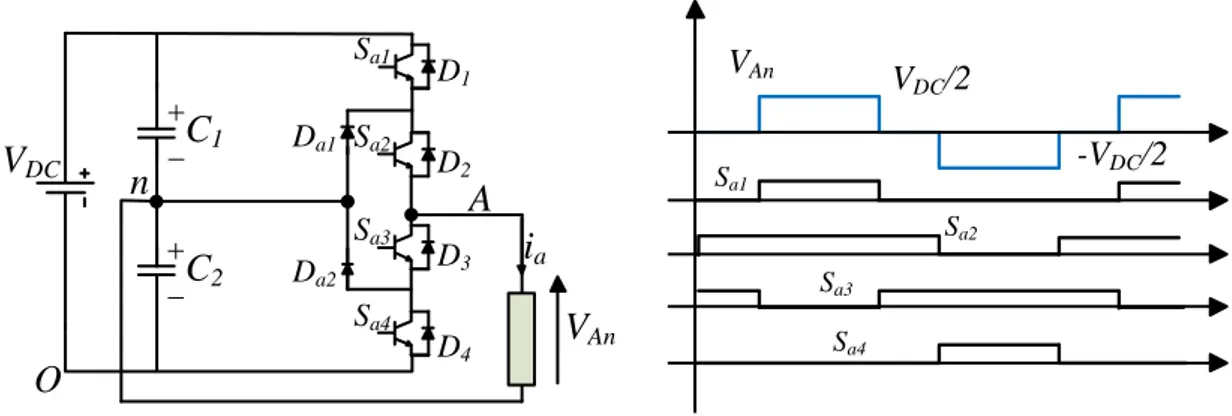
The conventional 3L-NPC inverter is shown in Fig. 1. 3. The DC-Bus voltage VDC is split into three levels
by two series-connected bulk capacitors C1 and C2. The middle point of the two capacitors n is defined as the
neutral point. In order to show the switching states, a single phase 3L-NPC inverter and its associated output voltage waveform VAn are considered in Fig. 1. 4. The output voltage VAn assumes three voltage levels: VDC/2,
- VDC /2 and 0, as depicted in Tab. 1.2. For voltage level VDC /2, switches Sa1 and Sa2 need to be turned on; for
voltage level -VDC /2, switches Sa3 and Sa4 need to be turned on and for the 0-voltage level, switches Sa2 and Sa3
need to be turned on. The key components that distinguish this topology from a conventional two-level inverter are the clamped diode Da1 and Da2.
These two diodes clamp the switch voltage to half of the DC-Bus voltage. When both Sa1 and Sa2 turn on, the
voltage across A and 0 is VDC, i.e., VAO=VDC. In this case, Da2 balances out the voltage sharing between Sa3 and
Sa4 with Sa3 blocking the voltage across C1 and Sa4 blocking the voltage across C2. The difference between VAn
and VAO is the voltage across C2, which is VDC /2.
Fig. 1. 5 shows a 5L-NPC inverter and their switching states. In this case, the DC-Bus consists of four capacitors C1, C2, C3 and C4. Assuming a VDC DC-Bus voltage, the voltage across each capacitor is VDC /4, and
the voltage stress on each device will be limited to VDC /4 through clamping diodes. Fig. 1. 6 shows the output
voltage waveform which consists of four voltage levels: VDC /2, VDC /4, 0, - VDC /4 and - VDC /2. In order to
11
turning on switches Sa2, Sa3, Sa4 and Sa5. Voltage levels 0 and -VDC /4 are respectively obtained by turning onswitches Sa3, Sa4, Sa5, Sa6 and Sa4, Sa5, Sa6, Sa7. Finally, by turning on Sa5, Sa6, Sa7 and Sa8 a-VDC /2 voltage is
produced.
V
DCV
DC/2
V
DC/2
n
A
B
C
N
i
ai
bi
cS
a1S
a2S
a3S
a4S
b1S
b2S
b3S
b4S
c1S
c2S
c3S
c4D
a1D
a2D
b1D
b2D
c1D
c2C
1C
2Fig. 1. 3 Conventional three-phase 3L-NPC inverter
V
DCn
A
i
aS
a1S
a2S
a3S
a4D
a1D
a2C
1C
2V
AnD
1D
2D
3D
4O
V
An Sa1 Sa2 Sa3 Sa4V
DC/2
-V
DC/2
Fig. 1. 4 Conventional single-phase 3L-NPC inverter and associated waveform Table 1.2 Switching states for a 3L-NPC inverter
Sa1 Sa2 Sa3 Sa4 VAn Component conduction 1 1 0 0 VDC /2 If ia>0 Sa1, Sa2 If ia<0 D1, D2 0 1 1 0 0 If ia>0 Da1, Sa2 If ia<0 Da2, Sa3 0 0 1 1 -VDC /2 If ia>0 D4, D3 If ia<0 Sa3, Sa4
A p-phase n-level NPC inverter is equipped with 2p(n-1) switching devices, p(n-1)(n-2) clamping diodes and
(n-1) capacitors. Although each active device is only required to block a VDC /(n-1) voltage, the clamping
12
devices Sa5, Sa6, Sa7 and Sa8 are turned on, Da2 needs to block three capacitor voltage, or 3VDC /4. Notice thatwhen the number of voltage levels n is sufficiently high, the number of switching devices and diodes will make the system impractical to implement.
Sa1 Sa2 Sa3 Sa4 Sa1 Sa2 Sa3 Sa4 VAO 1 1 1 1 0 0 0 0 VDC 0 1 1 1 1 0 0 0 3VDC /4 0 0 1 1 1 1 0 0 VDC /2 0 0 0 1 1 1 1 0 VDC /4 0 0 0 0 1 1 1 1 0 VDC A B C N ia ib ic Sa5 Sa6 Sa7 Sa8 Sb5 Sb6 Sb7 Sb8 Sc5 Sc6 Sc7 Sc8 C3 C4 n Sa1 Sa2 Sa3 Sa4 Sb1 Sb3 Sb4 Sc1 Sc2 Sc3 Sc4 Da1 Da2 C1 C2 Da3 Da4 Da5 Da6 Dc1 Dc2 Dc3 Dc4 Dc5 Dc6 Db1 Db2 Db3 Db4 Db5 Db6 O Sb2
Fig. 1. 5 Switching States for a conventional three-phase 5L-NPC inverter
S
a1S
a2S
a3S
a4V
DC/2
V
DC/4
-V
DC/4
-V
DC/2
Sa5
S
a6S
a7S
a8V
AnFig. 1. 6 Output voltage waveform for a 5L-NPC inverter
1.1.2 Flying Capacitor Inverter
Fig. 1. 7 depicts the fundamental building block of a three-phase three-level flying capacitor inverter. A major advantage of this topology is that it eliminates the clamping diode issues typical of the NPC topology. Additionally, this topology naturally limits the dv/dt stress across the devices and introduces additional
13
switching states that can be used to maintain the charge balance in the capacitors. Unlike the NPC, the FC topology has enough switching states to control the charge balance on each leg, even if the phase current is unidirectional. The voltage change between two adjoining capacitor legs gives the size of the voltage steps in the output waveform.
V
DCV
DC/2
V
DC/2
n
A
B
C
N
i
ai
bi
cS
a1S
a2S
a3S
a4S
b1S
b2S
b3S
b4S
c1S
c3S
c4C
1C
1C
1S
c2Fig. 1. 7 Conventional three-phase 3L-FC inverter
The output voltage inverter VAn in Fig. 1. 8 assumes three voltage levels: VDC /2, - VDC /2 and 0. In order to
obtain VDC /2, switches Sa1 and Sa2 need to be turned on, while -VDC /2, is produced by turning on switches Sa3
and Sa4 and a 0-voltage level is obtained by turning on Sa1-Sa3 or Sa2-Sa4. Clamping capacitor C1 is charged
when Sa1 and Sa3 are turned on, and is discharged when Sa2 and Sa4 are turned on. The charge of C1 can be
balanced by proper selection of the 0-level switch combination. Major advantages of the FC-MLI topology consist in making unnecessary the filter and the control of active and reactive power flows through phase redundancies.
However, troubles related to the capacitors voltage balance, as well as, to the initial capacitors charge procedure, in addition to a larger number of capacitors, disadvantage this topology. Moreover, on a FC inverter, capacitor voltages must be maintained within suitable limits. Thus, the capacitance of flying capacitors increases almost inversely with the switching frequency, making the FC topology impractical at low and medium switching frequencies (≥ 1500-1800 Hz).
The voltage synthesis in a FC converter has more flexibility than a NPC converter. Fig. 1. 9 shows a 5L-FC topology and the switching states. As an example, using the last diagram, the voltage of a five-level phase-leg A output referred to the neutral point n, VAn, can be synthesized by the following switch combinations.
14
2. Voltage level VDC /4: three possible combinations exist: a) Sa1, Sa2, Sa3, Sa5 are turned on and VAn=VDC/2 of upper C1’s-VDC /4 of C1. b) Sa2, Sa3, Sa4, Sa8 are turned on and VAn= 3VDC /4 of C3’s,VDC /2 of
lower C4’s. c) Sa1, Sa3, Sa4, Sa7 are turned on and VAn= VDC /2 of upper C4’s, -3VDC /4 of lower C3’s+ VDC
/2 of C2’s.
3. 0-voltage level: six combinations exist: a) Sa1, Sa2, Sa5, Sa6 are turned on and VAn= VDC /2 of upper C4’s
-VDC /2 of C2’s. b) Sa3, Sa4, Sa7, Sa8 are turned on and VAn= VDC /2 of C2 -VDC /2 of lower C4. c) Sa1, Sa3,
Sa5, Sa7 are turned on and VAn= VDC /2 of upper C4’s-3VDC /4 of C3’s+ VDC /2 of C2’s-VDC /4 of C1. d)
Sa1, Sa4, Sa6, Sa7 are turned on and VAn= VDC /2 of upper C4’s-3VDC /4 of C3’s+VDC /4 of C1. e) Sa2, Sa4,
Sa6, Sa8 are turned on and VAn= 3VDC /4 of upper C3’s-3VDC /4 - VDC /4 of C2’s+VDC /4 of C1-VDC /2 of
lower C4’s. f) Sa2, Sa3, Sa5, Sa8 are turned on and VAn= 3VDC /4 of C3’s-VDC /4 of C1, VDC/2 of lower
C4’s.
4. Voltage level -VDC /4: three possible combinations exist: a) Sa1, Sa5, Sa6, Sa7 are turned on and VAn=VDC
/2 of upper C4’s-3VDC /4 of C3’s. b) Sa4, Sa6, Sa7, Sa8 are turned on and VAn= VDC /4 of C1, -VDC /2 of
lower C4’s. c) Sa3, Sa5, Sa7, Sa8 are turned on and VAn= VDC /2 of C2’s, -VDC /4 of C1-VDC /2 of lower C4’s.
5. Voltage level -VDC /2: all lower switches Sa5-Sa8 are turned on.
Sa1 Sa2 Sa3 Sa4 VAn 1 1 0 0 VDC /2 1 0 1 0 0 0 1 0 1 0 0 0 1 1 -VDC /2
V
AnS
a1S
a2S
a3S
a4V
DC/2
-V
DC/2
Fig. 1. 8 Switching states for a 3L-FC inverter
By proper selection of capacitor combinations, it is possible to balance the capacitor charge. Similarly, to the NPC inverter, the FC requires a large number of bulk capacitors to clamp the voltage. In an n-level structure, the FC inverter requires (n-1) DC-link capacitors and (n-1) (n-2)/2 auxiliary capacitors per phase compared to NPC-MLI topology. The auxiliary capacitors are pre-charged to the voltage levels of VDC /4,
15
Sa1 Sa2 Sa3 Sa4 Sa1 Sa2 Sa3 Sa4 VAO 1 1 1 1 0 0 0 0 VDC 1 1 1 0 1 0 0 0 3VDC /4 1 1 0 0 1 1 0 0 VDC /2 1 0 0 0 1 1 1 0 VDC /4 0 0 0 0 1 1 1 1 0 V
DCA
B
C
N ia ib ic Sa5 Sa6 Sa7 Sa8 Sb5 Sb6 Sb7 Sb8 Sc5 Sc6 Sc7 Sc8 C1 C1 n Sa1 Sa2 Sa3 Sa4 Sb1 Sb3 Sb4 Sc1 Sc2 Sc3 Sc4 C1 C1 O Ca1 Ca2 Ca3 Ca4 Ca5 Ca6 Cb1 Cb2 Cb3 Cb4 Cb5 Cb6 Cc1 Cc2 Cc3 Cc4 Cc5 Cc6 Sb2Fig. 1. 9 A conventional 5L-FC inverter with Switching states
1.1.3 Cascaded H-Bridge Inverters
As earlier mentioned, the cascaded H-bridge inverter (CHB) has been the first multilevel converter, developed in the late 1960s [11]. This topology is based on the series connection of single-phase inverters with separate DC sources [17]. Fig. 1. 10 shows a 5-level CHB inverter composed by two isolated H-bridge inverters.
The resulting phase voltage is synthesized by combination of the voltages generated by the cells. Each single-phase full-bridge inverter generates three output voltages levels: VDC, -VDC, and 0. This is made possible by
connecting the capacitors sequentially to the AC side via the four power switches. The resulting output AC voltage swings from -2VDC to 2VDC with 5 steps. The obtained staircase waveform is nearly sinusoidal, even
without filtering. The switch power and the stored energy are reduced to about 80%, if compared to an NPC inverter.
However, a complex grid transformer, a large number of isolated power supplies, increased DC-link capacitances and a large number of semiconductor devices are major drawbacks of the CHB-MLI [41]-[42].
This topology has been used for active filter and reactive power compensation, electric vehicles, PV power conversion [42], Uninterruptible Power Supplies (UPSs), and magnetic resonance imaging etc. CHB-MLIs have been previously designed for static VAR compensators.
16
V
DCV
DCV
AnA
A
V
C2V
C1 Vc1 Vc2 2VDC VDC -VDC -2VDC VAnFig. 1. 10 Cascaded 5L-CHB inverter
Table 1.3 Main features of MLIs
Topology NPC FC CHB
Switching Devices 2(n-1) 2(n-1) 2(n-1) Clamping diodes per phase (n-1) (n-2) 0 0
DC.Bus Capacitors (n-1) (n-1) Depends on type of supply Balancing Capacitor per phase 0 (n-1) -
Voltage unbalancing Average High Very small Applications Motor drive
systems STATCOM
Motor drive systems STATCOM
Motor drive system, PV, fuel cells, battery system
1.1.4 Recent advances in MLI topologies
Advanced multilevel converters have been proposed in literature [41]. Among them, the following have found practical application:
five-level H-bridge NPC (5L-HNPC)
three-level active NPC (3L-ANPC)
five level active NPC (5L-ANPC)
modular multilevel converter (MMC)
cascaded matrix converter (CMC)
transistor-clamped converter (TCC)
17
cascaded NPC feeding open-end loads
hybrid NPC-CHB and hybrid FCCHB topologies
stacked FC or stacked multi-cell
These topologies are variations of the three classic topologies discussed in the previous section, as shown in Fig. 1. 2. Technical specifications are available in [11]-[25]. The 5L-HNPC converter is composed of the H-bridge connection of two classic 3L-NPC phase legs, as shown in Fig. 1. 11, forming a 5L-HNPC converter. This converter is found in practice with a 36-pulse rectifier system featuring IGCT devices, for the 2–7-MW (air cooled) or 5–22-MW (water cooled) power range. Several 5L-HNPC configurations have been developed with 24- or 36-pulse diode rectifier front ends, with medium-voltage IGBTs (MV-IGBTs), IEGTs, or GCTs, up to 7.8-kV output voltage, 120-Hz output frequency and 120 MVA output power [13]. Fig. 1. 12a shows a 3L-NPC inverter equipped with IGCTs, rating 20–200 MVA. One of the drawbacks of the 3L-NPC topology is the unequal share of losses between the inner and outer switching devices in each converter leg. Recently, a variation of the ANPC concept has been proposed, i.e., a five-level hybrid multilevel converter that combines a 3L-ANPC leg with a three-level FC power cell connected between the internal ANPC switching devices, as shown in Fig. 1. 12b. Although it is a hybrid topology, it has been called 5L-ANPC [48]–[50], [53]. Note that, instead of IGCTs, series-connected IGBTs are used in the NPC part of the converter, probably to keep all semiconductors of the same type. A commercial version of this topology has recently been introduced [11], [50], aimed to medium voltage, low-medium power applications. A variation of the hybrid 5L-ANPC has been proposed by adding a common cross converter (CCC) stage [55] to the 5L-ANPC, resulting in a nine-level hybrid converter [51], as shown in Fig. 1. 12c. Although this additional stage increases the number of levels, greatly improving the power quality, this comes at the expense of a quite complex structure and the need to balance both the CCC and FC capacitor voltages. Another multilevel converter that has recently found industrial applications, particularly for HVDC systems, is the MMC (also known as M2C) [56], [57]. Basically, the MMC is composed of series connected single-phase two-level voltage source converter (2L-VSC) legs, as illustrated in Fig. 1. 13(left). This topology found practical application on 200 power-cell/phase structures reaching 400 MW [55] and 1 GW [56]. The Transistor-Clamped Converter TCC concept is very similar to that of the DCC, however, bidirectional switches are used instead of diodes to clamp the connection points between switches and capacitors, Fig. 1. 13 (right). This gives a controllable path for the currents through the clamping devices, like the ANPC. This topology has been exploited [15], [58] in medium voltage (3.3, 6.6, and 9.9 kV) and high power (up to 48 MW) industrial applications. Power losses are shared among the devices,
18
enabling higher switching frequencies, thus increasing the maximum output frequency and making this converter suitable for variable high-speed drives, in railway traction applications.
V
DCV
DC/2
V
DC/2
n
V
DCV
DC/2
V
DC/2
n
V
DCV
DC/2
V
DC/2
n
A
B
C
6-Pulse rectifier 6-Pulse rectifier Three-phase transformerV
DC +-Fig. 1. 11 Three-phase 5L-HNPC inverter [43]-[45]
V
DC/2
V
DC/2
n
A
V
DCIGCT
V
DCV
DC/2
V
DC/2
V
DC/4
A
V
DCV
DC/2
V
DC/2
V
DC/4
A
V
DC/8
(a)
(b)
(c)
Fig. 1. 12 Active NPC. a) 3L-ANPC featuring IGCTs [46]-[47]. b) 5L-ANPC featuring IGBTs [48]-[50]. c) CCC stage plus 5L-ANPC hybrid nine-level inverter [51]
19
DC/AC DC/AC DC/AC VDC
DC/AC DC/AC DC/AC DC/AC
DC/AC
DC/AC DC/AC DC/AC DC/AC DC/AC + -Power cell A B C VDC VDC/2 VDC/2 n A B C MV-IGBT
Fig. 1. 13 Modular Multilevel converter MMC (left), Three phase three-level TCC(right)
The combination of different multilevel converter topologies gives rise to hybrid multilevel converters. Two main hybrid multilevel converter are present in the literature, the NPC-CHB converter [59]-[65], depicted in Fig. 1. 14(left) and the Hybrid Multilevel Converters feeding Open-End Winding machine [66]-[81], Fig. 1. 14 (right).
The NPC-CHB, combines a 3L-NPC and single-phase H-bridge cells. On the H-bridge DC side a floating capacitor is present without a voltage supply. Hence, the addition of H-bridge stages only introduces more voltage levels but does not effectively increase the active power rating of the overall converter. The number of series connected H-bridge usually varies between one and two.
VDC + -A B C 3L-NPC DC/AC DC/AC VDC ’ + -Main NPC VDC ’’ + -Cond. NPC Open-end winding Machine
Fig. 1. 14 Multilevel NPC-CHB hybrid converter(left)[52]-[54], Cascaded NPC inverter connected in series through an open-end winding stator machine(right)
The concept of cascading two 3L-NPC converters, with one at each side of an open-end stator winding of an induction motor, was first introduced in [66]. Later, two separately excited two-level voltage source inverters (2L-VSIs) with different voltage ratios generating a four-level converter were introduced [69]. This concept evolved in a structure encompassing a MLI and a TLI. The first (the main inverter) supplies only active power to the load, while the second (the auxiliary inverter) acts as a series active filter [67]-[70]. In this way, high voltage power devices are adopted for the main inverter and low voltage fast power devices can be used on the auxiliary one.
20
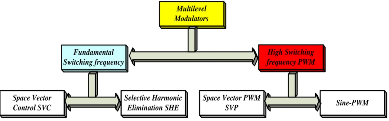
1.1.5 Control and Modulation Strategy for MLIs
Modulation strategies for multilevel inverters can be divided into two main groups, namely: space vector and time domain, Fig. 1. 15. Furthermore, they can be classified according to switching frequency, as shown in Fig. 1. 16 [82], [83]. A very popular modulation strategy, largely used in industrial applications, is the classic carrier-based sinusoidal PWM (Sine-PWM) that uses the phase-shifting technique to reduce output voltage harmonics [17], [84], [85]. An interesting alternative is the Space Vector Modulation SVM strategy [82].
Strategies which work at low switching frequencies, generating a staircase output voltage waveform are the multilevel selective harmonic elimination [86], [87] and the space-vector control (SVC) [88]. Generally, a low-switching frequency features low switching losses while high-switching frequency features high switching losses.
Fig. 1. 15 Classification of Multilevel modulation methods based on the domain in which they operate
Multilevel Modulators Fundamental Switching frequency High Switching frequency PWM Sine-PWM Space Vector PWM SVP Selective Harmonic Elimination SHE Space Vector Control SVC
21
1.1.5.1
Sine-PWM Modulation
The most popular control technique for traditional inverters is the sinusoidal or “subharmonic” Pulse Width Modulation (SPWM). Its popularity is due to the easy implementation and the robustness [89]. When a single triangular carrier signal is used on a conventional three-phase two-level inverter, n-1 carriers will be needed on a n-level inverter in order to synthetize the pseudo-sinusoidal output voltage. In the last case, the carriers have the same frequency fc, the same peak-to-peak amplitude Ac, and are deployed on contiguous bands. The
phase displacement between two contiguous triangular carriers is free. Three configurations can be used, Fig. 1. 17:
All the carriers are in opposition with the following one (APOD disposition, see Fig. 1. 17(left))
All the carriers above the zero value reference are in phase among them, but in opposition with those located below the zero level (POD disposition, see Fig. 1. 17(middle))
All the carriers are in phase among them (PH disposition, see Fig. 1. 17(right)).
-1 -0.5 0 0.5 1 -1 -0.5 0 0.5 1 -1 -0.5 0 0.5 1
Fig. 1. 17 Carriers and reference waveforms for 5-level inverter. Left) APOD. Middle) POD. Right) PHD.
The amplitude modulation index ma and the frequency ratio mf are defined as:
being Am and fm respectively the peak-to-peak amplitude of the fundamental voltage and the fundamental
frequency. The harmonic content of the output voltage varies according to the selected configuration. In the APO and PO cases, the harmonics at the carrier frequency and multiples do not exist at all. For the PHD, no harmonics exist at even multiples of the carrier frequency. When the frequency ratio mf is high, there are no
substantial differences among the three configurations, because all the harmonics are moved to the high frequency range so they are easily filtered. The scenario changes when mf is not sufficiently high. In this case
the PH configuration seems the least interesting, due to large (greater than the fundamental) harmonic at fc,
Ac n Am m a ( 1) (1.1) fc fm m f (1.2)
22
generated at low ma values. However, dealing with three-phase inverters and using a single-phase modulation,that harmonic is of common mode nature, so it will not be present in the harmonic content of the phase current of a wye connected load. In this case the PH configuration becomes the most interesting one, due to the very little amplitude of the other harmonics. On a multilevel SPWM the apparent switching frequency of the output voltage is a multiple of the switching frequency of each cell. Such an advantageous feature allows a reduction of the effective switching frequency, thus reducing the switching losses.
1.1.5.2
Space Vector Modulation
According to the space vector modulation, the reference voltage Vs is synthetized by forcing the inverter to assume a suitable sequence of states (or voltage vectors) [90], [91]. Fig. 1. 18 shows the allowable states for a three-level inverter. A common characteristic to all SVM-based schemes is that the modulation algorithm is divided into three stages. In the first, a set of voltage vectors are selected, usually, the three closest to the reference voltage vector. On the second stage duty cycles are computed (or On and Off times) for each vector in order to achieve the desired reference voltage as average over a single switching time (the inverse of the switching frequency). In the final stage the vector sequence is generated.
b
c
B C D E F K J I H S R P N M L 1 Aa
V
s G O QV
j+1V
jV
j+2Fig. 1. 18 Space vector for a 3LI inverter.
The desired voltage vector can be synthesized by computing the duty cycles (Tj, Tj+1 and Tj+2) of the three
23
SVPWM methods generally feature good utilization of DC-link voltage, low current ripple, and an easy hardware implementation by a digital signal processor (DSP). These features make it suitable for high voltage, high-power applications. As the number of levels increases, redundant switching states and the complexity of selection of switching states increase dramatically.1.1.5.3
Selective Harmonic Elimination
The selective harmonic elimination is considered as a low-frequency modulation [86], [87]. Fig. 1. 19 shows a generalized quarter-wave symmetric stepped-voltage waveform synthesized by a n-level inverter, being m the number of switching angles. By applying the Fourier series analysis, the amplitude of any odd harmonic of the stepped waveform can be expressed as:
V
MLIV
DC/2
-V
DC/2
V’
DC(n-1)
0
θ
1θ
mV
1Fig. 1. 19 Generalized output stepped-voltage waveform for a n-level inverter
where Vk is the kth level of DC voltage, n is the harmonic order and k is the kth switching angle. The amplitude
of the staircase output phase voltage VMLI is controlled by acting on m=(n-1)/2 switching angles 1,2,...,m
(0≤1<2<m)/2≤ π/2). More specifically, switching angles are selected in order to obtain the required
fundamental voltage reference V1, while eliminating from the harmonic content of the output voltage, n-1 of
the lowest odd, non-triple harmonics. Therefore, 1, 2,..., m, are computed by solving the following set of
(n-1)/2 non-linear transcendental equations:
T V j T j V j T j V s 1 1 (1.3)
m k k n V k n V n 1 ) cos( 4
(1.4)24
where: k is the order of the highest harmonic that has to be eliminated and ma is the modulation index definedas: DC
V
V
m
a*
4
(1.6)In general, the most significant low-frequency harmonics are selected for elimination, as high-frequency harmonic components can be readily removed by using additional filters.
1.1.5.4
Space Vector Control and Direct Torque Control
A conceptually different control method for multilevel inverters, based on the space-vector theory, is introduced in [83]. This control strategy, called Space Vector Control SVC, works with low switching frequencies. It is adopted for inverters with a large number of voltage levels, where voltage vectors are very close, as depicted in Fig. 1. 20.
b
c
a
V
sV
jV
jV
sFig. 1. 20 Space Vector locations for high number of level
0
cos
....
cos
cos
...
...
...
...
...
...
0
5
cos
....
5
cos
5
cos
cos
....
cos
cos
2 / ) 1 ( 2 1 2 / ) 1 ( 2 1 2 / ) 1 ( 2 1
n n a nk
k
k
m
(1.5)25
The basic principle of SVC is to generate a voltage vector that minimizes the space error, or distance to the reference vector Vs. The high density of vectors produced by the n-level inverter (n>11) will generate onlysmall space errors, a traditional PWM modulation strategy it is, therefore, unnecessary. The hexagon of Fig. 1. 20 shows the boundary of highest proximity, which allows to select the inverter voltage vector that is closest to the reference voltage vector. As the amount of inverter voltage levels drops, the SVC method becomes ineffective, as the space error raises, thus increasing the load current ripple. Finally, the DTC technique has been developed for low-voltage two-level inverters as an alternative to the field oriented method to effectively control torque and flux in ac drives [92]. DTC and hysteresis current control techniques have also been applied in multilevel inverters [93]. At least one major manufacturer has been selling medium-voltage three-level diode clamped inverters controlled with DTC [94].
1.1.5.5
Capacitor Balancing Techniques for MLIs
A typical issue of a MLI is the fluctuation of the neutral point of the DC-Bus, causing the distortion of the output voltage. This phenomenon is clearly discussed in [95]. The paper demonstrated that a diode-clamped multilevel inverter delivering only real power to the load cannot establish balanced voltages without admitting output voltage distortion. On the contrary, a voltage balancing method is not needed if a suitable reactive power is delivered to the load. Many techniques can be adopted in order to solve the problem of the fluctuation of the neutral point. In [96] the problem is solved by using a back to-back rectifier/inverter system and proper voltage balancing control. Other papers [97]–[99] suggested the use of additional voltage balancing circuits, such DC chopper, etc. The capacitor-clamped structure was originally proposed for high-voltage DC/DC conversions [100]. It is easy to balance the capacitor voltages in these applications because the load current is DC. Voltage balancing in a capacitor-clamped multilevel inverter, is a quite complex task [60], [101]. It has been shown theoretically that the capacitor-clamped inverter cannot self-balance the capacitor voltage when no real power is delivered to the load, such as in reactive power compensation. Moreover, voltage balancing become troublesome because each phase leg has its own floating capacitor. The cascaded multilevel inverter was first introduced for motor drive applications, exploiting an isolated and independent DC voltage source for each H-bridge [17]. However, a paper presented the idea of using cascade multilevel inverter for reactive and harmonic compensation, omitting isolated DC sources [96]. Additional works further demonstrated that the cascaded multilevel inverter is suitable for universal power conditioning in medium-voltage power systems [102], [103]. Such a configuration, in fact, provides lower costs, higher performance, less electromagnetic interference
26
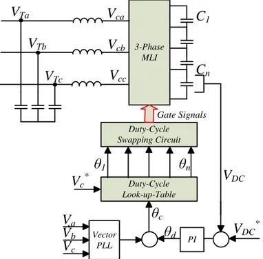
(EMI), and higher efficiency than the traditional PWM inverter for power line conditioning applications. Although the cascaded inverter has an inherent self-balancing characteristic, because of power losses and limited controller resolution, a slight voltage imbalance can occur. A simple control scheme, which ensures a DC voltage balance, has been proposed for reactive and harmonic compensation [96]. Fig. 1. 21 shows its control block diagram. It contains a proportional–integral (PI) regulator to adjust the trigger angle and to ensure zero steady state error between the reference DC voltage and the DC-bus voltage. Multilevel rectifiers have been also proposed to eliminate phase shift transformers. For those applications not requiring regenerative capabilities, simplified (or reduced) multilevel rectifiers have been proposed in [104]. This specific rectifier, named the Vienna rectifier, has been used for telecommunication power supplies. Fig. 1. 22 shows the per-phase leg structure for a three-level Vienna rectifier.3-Phase MLI Duty-Cycle Swapping Circuit Gate Signals Duty-Cycle Look-up-Table
θ
1θ
nV
DC*V
a PIθ
dθ
c Vector PLLV
bV
cV
c*V
DCV
caV
cbV
ccV
TaV
TbV
TcC
1C
nFig. 1. 21 Control diagram for DC-Bus voltage control in a MLI
to 3NPC
V
DC27
1.2 References of Chapter 1
[1] J. Rodriguez, J.-S. Lai, and F. Z. Peng, “Multilevel inverters: A survey of topologies, controls, and applications,” IEEE Trans. Ind. Electron., vol. 49, no. 4, pp. 724–738, Aug. 2002.H. Stemmler, “High-power industrial drives,” IEEE Proc., vol. 82, pp. 1266-1286, Aug. 1994.
[2] S. Rizzo and N. Zargari, “Medium voltage drives: What does the future hold?” in Proc. 4th IPEMC Conf., Aug. 14–16, 2004, vol. 1, pp. 82–89.
[3] R. D. Klug and N. Klaassen, “High power medium voltage drives—Innovations, portfolio, trends,” in Proc. Eur. Conf. Power Electron. Appl., 2005, pp. 1–10.
[4] B. Wu, High-Power Converters and AC Drives. New York: Wiley-IEEE Press, Mar. 2006
[5] J. Rodriguez, S. Bernet, B. Wu, J. O. Pontt, and S. Kouro, “Multilevel voltage-source-converter topologies for industrial medium-voltage drives,” IEEE Trans. Ind. Electron., vol. 54, no. 6, pp. 2930–2945, Dec. 2007.
[6] P. Steimer, “High power electronics, trends of technology and applications,” in Proc. PCIM, Germany, May 2007.
[7] L. G. Franquelo, J. Rodriguez, J. I. Leon, S. Kouro, R. Portillo, and M. A. M. Prats, “The age of multilevel converters arrives,” IEEE Ind. Electron. Mag., vol. 2, no. 2, pp. 28–39, Jun. 2008.
[8] J. Rodriguez, B. Wu, S. Bernet, N. Zargari, J. Rebolledo, J. Pontt, and P. Steimer, “Design and evaluation criteria for high power drives,” in Conf. Rec. IEEE IAS Annu. Meeting, Oct. 5–9, 2008, pp. 1–9.
[9] J. Rodriguez, L. G. Franquelo, S. Kouro, J. I. Leon, R. C. Portillo, M. A. M. Prats, and M. A. Perez, “Multilevel converters: An enabling technology for high-power applications,” Proc. IEEE, vol. 97, no. 11, pp. 1786–1817, Nov. 2009.
[10] B. K. Bose, “Power electronics and motor drives recent progress and perspective,” IEEE Trans. Ind. Electron., vol. 56, no. 2, pp. 581–588, Feb. 2009.
[11] W. McMurray, “Fast response stepped-wave switching power converter circuit,” U.S. Patent 3 581 212, May 25, 1971.
[12] J. A. Dickerson and G. H. Ottaway, “Transformerless power supply with line to load isolation,” U.S. Patent 3 596 369, Aug. 3, 1971. [13] R. H. Baker, “High-voltage converter circuit,” U.S. Patent 4 203 151, May 13, 1980.
[14] A. Nabae, I. Takahashi, and H. Akagi, “A new neutral-point-clamped PWM inverter,” IEEE Trans. Ind. Appl., vol. IA-17, no. 5, pp. 518–523, Sep./Oct. 1981.
[15] R. H. Baker, “Bridge converter circuit,” U.S. Patent 4 270 163, May 26, 1981.
[16] M. Marchesoni, M. Mazzucchelli, and S. Tenconi, “A non-conventional power converter for plasma stabilization,” in Proc. IEEE 19th Power Electron. Spec. Conf., Apr. 11–14, 1988, pp. 122–129.
[17] P.W. Hammond, “A new approach to enhance power quality for medium voltage drives,” in Proc. Ind. Appl. Soc. 42nd Annu. Petroleum Chem. Ind. Conf., Sep. 11–13, 1995, pp. 231–235.
[18] T. Meynard and H. Foch, “Dispositif électronique de conversion d’énergie électrique,” French Patent 267 971 5B1, Jan. 29, 1993. [19] ABB. [Online]. Available: www.abb.com
[20] SIEMENS. [Online]. Available: www.siemens.com [21] TMEIC-GE. [Online]. Available: www.tmeic-ge.com
28
[22] Ansaldo Sistemi Industriali. [Online]. Available: www.asiansaldo.com [23] Converteam. [Online]. Available: www.converteam.com
[24] Eaton. [Online]. Available: www.eaton.com
[25] Arrowspeed. [Online]. Available: www.arrowspeed.com [26] Ingeteam. [Online]. Available: www.ingeteam.com [27] WEG. [Online]. Available: www.weg.net
[28] Rongxin Power Electronic Co. (RXPE). [Online]. Available:www.rxpe.co.uk [29] LS Industrial Systems. [Online]. Available: http://eng.lsis.biz/
[30] Yaskawa. [Online]. Available: www.yaskawa.eu.com
[31] Beijing Leader & Harvest Electric Technologies. [Online]. Available:www.ld-harvest.com [32] Schneider-Electric. [Online]. Available: www.schneider-electric.com
[33] Alstom. [Online]. Available: www.alstom.com [34] Grupo Jema. [Online]. Available: www.grupojema.com
[35] D. Krug, S. Bernet, S. S. Fazel, K. Jalili, and M. Malinowski, “Comparison of 2.3-kv medium-voltage multilevel converters for industrial medium voltage drives,” IEEE Trans. Ind. Electron., vol. 54, no. 6, pp. 2979–2992, Dec. 2007.
[36] S. S. Fazel, S. Bernet, D. Krug, and K. Jalili, “Design and comparison of 4-kv neutral-point-clamped, flying-capacitor, and series-connected H-bridge multilevel converters,” IEEE Trans. Ind. Appl., vol. 43, no. 4, pp. 1032–1040, Jul./Aug. 2007.
[37] K. D. Papastergiou, P. W. Wheeler, and J. C. Clare, “Comparison oflosses in multilevel converters for aerospace applications,” in Proc. IEEE Power Electron. Spec. Conf., Jun. 15–19, 2008, pp. 4307–4312.
[38] M. Marchesoni and P. Tenca, “Theoretical and practical limits in multilevel npc inverters with passive front ends,” in Proc. EPE, Graz, Austria, Aug. 2001.
[39] J. Pou, R. Pindado, and D. Boroyevich, “Voltage-balance limits in fourlevel diode-clamped converters with passive front ends,” IEEE Trans. Ind. Electron., vol. 52, no. 1, pp. 190–196, Feb. 2005.
[40] S. Busquets-Monge, S. Alepuz, J. Bordonau, and J. Peracaula, “Voltage balancing control of diode-clamped multilevel converters with passive front-ends,” IEEE Trans. Power Electron., vol. 23, no. 4, pp. 1751–1758, Jul. 2008.
[41] S. Kouro, M. Malinowski, K. Gopakumar, J. Pou, L. G. Franquelo, BinWu, J. Rodriguez, M. A. Pérez, J. I. Leon, “Recent Advances and Industrial Applications of Multilevel Converters,” IEEE Trans. Ind. Electr., vol. 52, no. 8, pp. 2553–2580, Aug. 2010. [42] J. Rodríguez, Jih-Sheng Lai, F. Zheng Peng, “Multilevel Inverters: A Survey of Topologies Controls, and Applications,” IEEE Trans.
Ind. Electr., vol. 49, no. 4, pp. 724–738, Aug. 2002.
[43] Z. Cheng and B. Wu, “A novel switching sequence design for five-level NPC/H-bridge inverters with improved output voltage spectrum and minimized device switching frequency,” IEEE Trans. Power Electron., vol. 22, no. 6, pp. 2138–2145, Nov. 2007. [44] I. Etxeberria-Otadui, A. L. de Heredia, J. San-Sebastian, H. Gaztaaga, U. Viscarret, and M. Caballero, “Analysis of a H-NPC topology
for an AC traction front-end converter,” in Proc. 13th EPE-PEMC, Sep. 1–3, 2008, pp. 1555–1561.
[45] V. Guennegues, B. Gollentz, L. Leclere, F. Meibody-Tabar, and S. Rael, “Selective harmonic elimination PWM applied to H-bridge topology in high speed applications,” in Proc. Int. Conf. POWERENG, Mar. 18–20, 2009, pp. 152–156.
29
[46] T. Bruckner, S. Bernet, and H. Guldner, “The active NPC converter and its loss-balancing control,” IEEE Trans. Ind. Electron., vol. 52, no. 3, pp. 855–868, Jun. 2005.
[47] O. Apeldoorn, B. Odegard, P. Steimer, and S. Bernet, “A 16 MVA ANPC-PEBB with 6 ka IGCTs,” in Conf. Rec. 40th IEEE IAS Annu. Meeting, Oct. 2–6, 2005, vol. 2, pp. 818–824.
[48] J. Meili, S. Ponnaluri, L. Serpa, P. K. Steimer, and J. W. Kolar, “Optimized pulse patterns for the 5-level ANPC converter for high speed high power applications,” in Proc. 32nd IEEE IECON, Nov. 6–10, 2006, pp. 2587–2592.
[49] L. A. Serpa, P. M. Barbosa, P. K. Steimer, and J. W. Kolar, “Fivelevel virtual-flux direct power control for the active neutral-point clamped multilevel inverter,” in Proc. IEEE Power Electron. Spec. Conf., Jun. 15–19, 2008, pp. 1668–1674.
[50] F. Kieferndorf, M. Basler, L. A. Serpa, J.-H. Fabian, A. Coccia, and G. A. Scheuer, “A new medium voltage drive system based on anpc- 5l technology,” in Proc. IEEE-ICIT, Viña del Mar, Chile, Mar. 2010, pp. 605–611.
[51] T. Chaudhuri, P. Steimer, and A. Rufer, “Introducing the common cross connected stage (c3s) for the 5l ANPC multilevel inverter,” in Proc. IEEE Power Electron. Spec. Conf., Jun. 15–19, 2008, pp. 167–173.
[52] P. Steimer and M. Veenstra, “Converter with additional voltage addition or substraction at the output,” U.S. Patent 6 621 719, Sep. 16, 2003.
[53] M. Veenstra and A. Rufer, “Control of a hybrid asymmetric multilevel inverter for competitive medium-voltage industrial drives,” IEEE Trans. Ind. Appl., vol. 41, no. 2, pp. 655–664, Mar./Apr. 2005.
[54] K. A. Corzine and S. Lu, “Comparison of hybrid propulsion drive schemes,” in Proc. IEEE Elect. Ship Technol. Symp., Jul. 25–27, 2005, pp. 355–362.
[55] T. Chaudhuri, P. Barbosa, P. Steimer, and A. Rufer, “Cross-connected intermediate level (CCIL) voltage source inverter,” in Proc. IEEE Power Electron. Spec. Conf., Jun. 17–21, 2007, pp. 490–496.
[56] B. Gemmell, J. Dorn, D. Retzmann, and D. Soerangr, “Prospects of multilevel VSC technologies for power transmission,” in Proc. IEEE/PES T&D Conf. Expo., Apr. 21–24, 2008, pp. 1–16.
[57] SIEMENS, Introduction to HVDC Plus. [Online]. Available: https://www.energy-portal.siemens.com/static/hq/en/products_solutions/ 1 652_kn03011203.html
[58] B. Gollentz and V. Guennegues, “Three-level inverter,” U.S. Patent 20 100 084 922, Apr. 8, 2009.
[59] P. Steimer and M. Veenstra, “Converter with additional voltage addition or substraction at the output,” U.S. Patent 6 621 719, Sep. 16, 2003.
[60] M. Veenstra and A. Rufer, “Control of a hybrid asymmetric multilevel inverter for competitive medium-voltage industrial drives,” IEEE Trans. Ind. Appl., vol. 41, no. 2, pp. 655–664, Mar./Apr. 2005.
[61] K. A. Corzine and S. Lu, “Comparison of hybrid propulsion drive schemes,” in Proc. IEEE Elect. Ship Technol. Symp., Jul. 25–27, 2005, pp. 355–362.
[62] C. Silva, S. Kouro, J. Soto, and P. Lezana, “Control of a hybrid multilevel inverter for current waveform improvement,” in Proc. IEEE Int. Symp. Ind. Electron., Jun. 30–Jul. 2008, pp. 2329–2335.
[63] J. A. Ulrich and A. R. Bendre, “Floating capacitor voltage regulation in diode clamped hybrid multilevel converters,” in Proc. IEEE ESTS, Apr. 20–22, 2009, pp. 197–202.
30
[64] Z. Du, L. M. Tolbert, J. N. Chiasson, and B. Ozpineci, “A cascade multilevel inverter using a single DC source,” in Proc. 21st Annu. IEEE APEC, Mar. 19–23, 2006, pp. 426–430.
[65] S. Vazquez, J. I. Leon, L. G. Franquelo, J. J. Padilla, and J. M. Carrasco, ‘’DC-voltage-ratio control strategy for multilevel cascaded converters fed with a single DC source,” IEEE Trans. Ind. Electron., vol. 56, no. 7, pp. 2513–2521, Jul. 2009.
[66] H. Stemmler and P. Guggenbach, “Configurations of high-power voltage source inverter drives,” in Proc. 5th EPE, 1993, vol. 5, pp. 7–14.
[67] K. A. Corzine, M. W. Wielebski, F. Z. Peng, and J. Wang, “Control of cascaded multilevel inverters,” IEEE Trans. Power Electron., vol. 19, no. 3, pp. 732–738, May 2004.
[68] X. Kou, K. A. Corzine, and M. W. Wielebski, “Overdistention operation of cascaded multilevel inverters,” IEEE Trans. Ind. Appl., vol. 42, no. 3, pp. 817–824, May/Jun. 2006.
[69] K. A. Corzine, S. Lu, and T. H. Fikse, “Distributed control of hybrid motor drives,” IEEE Trans. Power Electron., vol. 21, no. 5, pp. 1374– 1384, Sep. 2006.
[70] S. Lu and K. A. Corzine, “Advanced control and analysis of cascaded multilevel converters based on P-Q compensation,” IEEE Trans. Power Electron., vol. 22, no. 4, pp. 1242–1252, Jul. 2007.
[71] V. T. Somasekhar, K. Gopakumar, M. R. Baiju, K. K. Mohapatra, and L. Umanand, “A multilevel inverter system for an induction motor with open-end windings,” IEEE Trans. Ind. Electron., vol. 52, no. 3, pp. 824– 836, Jun. 2005.
[72] S. Lu and K. Corzine, “Multilevel multi-phase propulsion drives,” in Proc. IEEE Elect. Ship Technol. Symp., Jul. 25–27, 2005, pp. 363–370.
[73] R. S. Kanchan, P. N. Tekwani, and K. Gopakumar, “Three-level inverter scheme with common mode voltage elimination and dc link capacitor voltage balancing for an open-end winding induction motor drive,” IEEE Trans. Power Electron., vol. 21, no. 6, pp. 1676– 1683, Nov. 2006.
[74] P. N. Tekwani, R. S. Kanchan, and K. Gopakumar, “A dual five-level inverter-fed induction motor drive with common-mode voltage elimination and dc-link capacitor voltage balancing using only the switchingstate redundancy—Part I,” IEEE Trans. Ind. Electron., vol. 54, no. 5, pp. 2600–2608, Oct. 2007.
[75] P. N. Tekwani, R. S. Kanchan, and K. Gopakumar, “A dual five-level inverter-fed induction motor drive with common-mode voltage elimination and dc-link capacitor voltage balancing using only the switchingstate redundancy—Part II,” IEEE Trans. Ind. Electron., vol. 54, no. 5, pp. 2609–2617, Oct. 2007.
[76] G. Mondal, K. Gopakumar, P. N. Tekwani, and E. Levi, “A reducedswitch- count five-level inverter with common-mode voltage elimination for an open-end winding induction motor drive,” IEEE Trans. Ind. Electron., vol. 54, no. 4, pp. 2344–2351, Aug. 2007. [77] D. Casadei, G. Grandi, A. Lega, and C. Rossi, “Multilevel operation and input power balancing for a dual two-level inverter with
insulated DC sources,” IEEE Trans. Ind. Appl., vol. 44, no. 6, pp. 1815–1824, Nov./Dec. 2008.
[78] M. Rotella, G. Penailillo, J. Pereda, and J. Dixon, “PWM method to eliminate power sources in a nonredundant 27-level inverter for machine drive applications,” IEEE Trans. Ind. Electron., vol. 56, no. 1, pp. 194– 201, Jan. 2009.
[79] G. Mondal, K. Sivakumar, R. Ramchand, K. Gopakumar, and E. Levi, “A dual seven-level inverter supply for an open-end winding induction motor drive,” IEEE Trans. Ind. Electron., vol. 56, no. 5, pp. 1665–1673, May 2009.
![Fig. 2. 25. ZSV V O’O’’ for Isolated Symmetrical Dual-Two Level Inverter in [8] with Sine-PWM modulation](https://thumb-eu.123doks.com/thumbv2/123dokorg/4584793.38863/48.892.145.811.166.428/fig-isolated-symmetrical-dual-level-inverter-sine-modulation.webp)
![Fig. 2. 31. Phase voltage and phase current in a Dual-two level Inverter proposed in [32]](https://thumb-eu.123doks.com/thumbv2/123dokorg/4584793.38863/50.892.149.807.574.898/phase-voltage-phase-current-dual-level-inverter-proposed.webp)
![Fig. 2. 36 . Phase voltage and phase current. a) Single DC-Bus voltage [51]. b) Isolated DC-Buses](https://thumb-eu.123doks.com/thumbv2/123dokorg/4584793.38863/54.892.162.805.397.840/phase-voltage-phase-current-single-voltage-isolated-buses.webp)