UNIVERSITÀ DEGLI STUDI DI ROMA
"TOR VERGATA"
FACOLTA' DI INGEGNERIA
DOTTORATO DI RICERCA IN
INGEGNERIA DEI SISTEMI SENSORIALI E DI APPRENDIMENTO
XXI CICLO DEL CORSO DI DOTTORATO
Study and Optimization of Polariton LASERs
Eleonora Petrolati
A.A. 2007/2008
Tutor: Prof. Aldo Di Carlo - Dr. Andrea Reale
Coordinatore: Prof. Corrado Di Natale
Trust I seek and I find in you Every day for us something new Open mind for a different view And nothing else matters
i
Index
Index ………...………...… i
Abstract ………...………..…… iv
Chapter 1 – Background and motivation ………...….…… 1
1.1 Scientific background ………..……….………… 4
1.1.1 Microcavities and Polaritons …………..……….…….………… 4
1.1.2 Microcavities as OPAs ……….…....……… 9
1.1.3 The need for wide band gap materials ………..…………..……….……… 9
1.1.4 Simulation softwares ………...……...… 11
References ……….………...….…… 13
Chapter 2 – Device simulation ………...…… 15
2.1 TiberCad ……….………....…… 15
2.1.1 The Exciton Model in TiberCad ……….………..…. 18
2.2 The simulation tool Dessis ……….………..……... 23
2.2.1 Upgrading of Dessis material parameter file ……….……… 26
ii
Chapter 3 - Design and optimization of GaN based LED
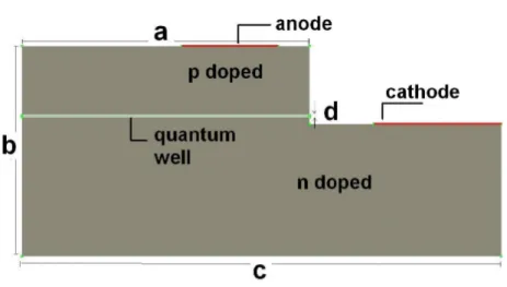
and Polariton Laser / VCSEL ……….…… 30
3.1 Influence of mesa contact dimension on the GaN/InGaN LED properties ...…….……… 30
3.2 Design of current confinement layer ………...…………...……… 36
3.3 The influence of mobility unbalance ………...……… 40
3.4 Enhancement of carrier focusing ………...……….… 45
3.5 Discussion on the inverted structure ………...………..…..… 50
3.6 Electrically injected bulk polariton laser ………...………...………..… 56
References ………...………..…… 60
Chapter 4 - Design of a new electrical injection polariton laser …….… 62
4.1 Why a new structure ………..………..……...…… 62
4.2 The patented design ………...………...…………..…… 61
References ………...………..… 66
Chapter 5 - Results of the StimScat Project (October 2008) ………...… 67
5.1 Microcavity properties and design ………...………...………..… 68
5.2 Observation of Polariton lasing at room temperature: optical injection …..…………...… 72
iii
References ………....………...………..… 77
Appendix A ………...………… 79
Appendix B ………...……… 82
Appendix C - List of publications and activities …….……...……….… 104
iv
Abstract
A polariton laser is a new concept of device based on the Bose Einstein condensation of cavity exciton-polaritons. It offers intrinsically high modulation speeds, low thresholds, long lifetime and low power consumption. Polariton lasing has been demonstrated at low and room temperature in optically pumped structures. Electrical injection of excitons and polaritons states have been reported for GaAs structures, while the realization of an electrically driven polariton laser is still missing.
The aim of the work presented in this thesis has been the modelling, design and optimization of GaN based devices, with regard to the aspects involved in the realization of the electrical injected polariton laser. To achieve these goals, a new simulation software has been developed to study the exciton transport in semiconductors and used together with conventional tools. Several simulations have been performed to understand the behaviour of GaN based light emitting diodes (LED), Vertical Cavity Vertical-cavity surface-emitting laser (VCSEL) and Polariton laser (PLASER) structures and new designs of GaN based devices have been proposed in order to optimize the electrical injection in GaN-based VCSELs/PLASERs and to achieve the polariton lasing in these structures. The strong interplay between carrier mobility, focussing efficiency and electrical injection has been carried for the first time.
The results of this work have received dissemination through 4 publications in international journals, presentations and posters at international conferences, and a patent concerning a new design for electrical injection in GaN based VCSELs/PLASERs. This work has been developed within the European Project StimScat (STIMulated SCATtering) started the 1st of September 2005 and ended the 1st of September 2008. The aim of the project was the realization of two new forms of opto-electronic device, namely the polariton laser and polariton-based micron-size optical parametric amplifier, both operating at room temperature.
v
Abstract
Il laser a polaritoni rappresenta una nuova classe di dispositivi basati sulla condensazione di Bose-Einstein di eccitoni-polaritoni in microcavità. Questo dispositivo prevede tra le caratteristiche principali un basso consumo di potenza, lunghi tempi di vita e basse tensioni di soglia. L'effetto laser dei polaritoni è stato dimostrato sia a basse temperature che a temperatura ambiente in strutture a pompaggio ottico. Inoltre, mentre l'iniezione elettrica di eccitoni e polaritoni è già stata dimostrata per strutture basate su GaAs, la realizzazione di un laser a polaritoni ad iniezione elettrica realizzato con GaN rimane ancora una sfida.
Lo scopo del lavoro di questa tesi è stato proprio progettare ed ottimizzare dispositivi basati su GaN, con particolare interesse agli aspetti coinvolti nella realizzazione del primo laser a polaritoni ad iniezione elettrica. Per raggiungere questo obiettivo, è stato sviluppato prima di tutto un nuovo simulatore in grado di studiare il trasporto di eccitoni nei semiconduttori. Sono state realizzate quindi diverse simulazioni per analizzare il comportamento di diodi ad emissione di luce (LED), laser a cavità verticale (VCSEL) e strutture per laser a polaritoni (PLASER) realizzati con GaN. Inoltre sono stati progettati nuovi design di dispositivi con lo scopo di ottimizzare l'iniezione elettrica nei VCSELs ed ottenere l'effetto laser dovuto ai polaritoni. Per la prima volta, è stata dimostrata la stretta interazione tra mobilità di portatori, efficienza di focusing e iniezione elettrica.
I risultati di questo lavoro sono stati pubblicati in riviste internazionali e presentati a diverse conferenze. Inoltre è stato realizzato un brevetto riguardante una nuova struttura per realizzare l'iniezione elettrica nei VCSEL e nei PLASER realizzati con GaN. Questo lavoro è stato sviluppato all'interno del progetto europeo StimScat (STIMulated SCATtering), che ha avuto inizio il primo Settembre 2005 ed è terminato il primo Settembre 2008. Lo scopo di questo progetto è stato la realizzazione di due nuovi dispositivi optoelettronici: il laser a polaritoni e il micro-amplificatore ottico parametrico a polaritoni, entrambi operanti a temperatura ambiente.
1
Chapter 1
Background and motivation
The semiconductor lasers have a wide range of use and represent an huge and evolving market. This development is linked with the advanced technology that allows the production of new types of lasers for new applications. Examples include the development of blue lasers, which opened the new market of Blue-ray DVD.
From a technical point of view, one of the main challenges imposed by the semiconductor lasers has been and is still to reduce their operating threshold. This threshold determines the energy consumption, but also the emission of heat which is fundamental for the integration of the components and their lifetimes.
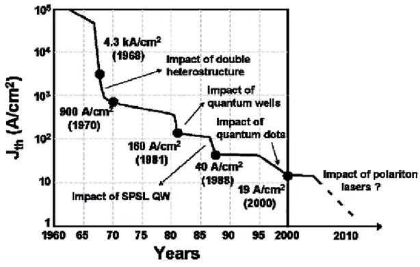
The first semiconductor laser produced fifty years ago had an extremely high current threshold, and for this reason they were unusable. Several revolutions based on the use of double heterostructures, quantum wells, vertical-emitting lasers (VCSEL) and quantum dots helped to reduce of several orders of magnitude the current threshold. Fig. 1.1 shows the evolution over time of the current threshold as it was presented by Z. Alferov (a double heterostructures developer and a Nobel Prize winner in 2000).
2
Recently a new kind of laser has been introduced based on Bose-Condensation of Polaritons, i.e the quasiparticle arising from the interaction between excitons and photons. Polaritons have a number of novel properties including scattering stimulated by final state occupancy, very light mass and new dispersions. Many new fundamental and applied opportunities arise from these properties. The high exciton binding energy and large oscillator strength of GaN provide the materials properties to achieve the realization of the Polariton laser even at rom temperature. At the same time GaN microcavity (MC) technology, required to correctly couple exciton and photons, is in its infancy and poses a number of challenges.
Although GaN devices are efficient light emitters, they have high thresholds for inversion due to the high carrier densities of states. MCs in the strong coupling regime overcome this intrinsic limitation, with up to 4 orders of magnitude lower density of states. Stimulation is thus much easier
Fig. 1.1 - Chronological evolution of the current threshold in semiconductor lasers shown by Alferov during his presentation for Nobel prize in 2000.
3
to attain, with the promise of low thresholds for coherent emission, an order of magnitude lower than present blue or ultra-violet semiconductor lasers.
The aim of the work presented in this thesis was the modeling, design and optimization of GaN based devices, with regard to the aspect involved in the realization of the first polariton laser. This work has been developed within the European Project StimScat (STIMulated SCATtering) started the 1st of September 2005 and ended the 1st of September 2008. The aim was to realize two new forms of opto-electronic device, namely the polariton laser and polariton-based micron-size optical parametric amplifier, both operating at room temperature.
While polariton lasing has been demonstrated by using all optical technique, the realization of an electrically driven polariton laser is still missing. There are several issues which have to be addressed for electrical injection such as efficient current injection, efficient exciton formation, contacting technologies, separate electron and hole injection etc.
The project assembled a collaboration from leading laboratories around Europe, with the necessary expertise:
• The University of Sheffield (USFD)
• Centre de Rechereche sur l'Hétéro-Epitaxie et ses Applications (CRHEA) • University of Strathclyde (U-Strath)
• Ecole Polytechnique Fédérale de Lausanne (EPFL) • University of Southampton (USTN)
• LASMEA, University Clermont-Ferrand II (LASMEA) • Sharp Laboratories of Europe (SLE)
• University of Rome “Tor Vergata” (Rome)
Stimscat focus on Gallium Nitride (GaN) based semiconductor microcavities (MCs) in which excitons and photons are strongly coupled together to form exciton-polariton coupled modes, to fabricate new forms of coherent light emitters and compact optical parametric amplifiers, with
4
major potential advantages over present-day technologies. These radically new device concepts have major potential advantages over present day technologies, in terms of low threshold, short wavelength coherent emission and low power operation.
The specific overall objectives of StimScat were:
• The design, fabrication and testing of the first polariton laser at room temperature. The demonstration of this new form of coherent light source would represent a major breakthrough on the international scale with implications for both pure and applied science. It also corresponds to the achievement of Bose condensation in a solid state material, an equally significant fundamental advance. The research focus on both optical and electrical injection. The research on electrical injection structures have additional wide relevance to the development of GaN-based resonant cavity LEDs and VCSEL structures.
• In similar structures demonstrate ultrafast optical parametric amplifier (OPA) operation at room temperature and above in compact micron size devices, as opposed to the mm-cm scale in standard OPAs.
The field of polariton physics and of stimulated scattering in semiconductors is one which has been pioneered by European scientists.
1.1 Scientific
background
1.1.1 Microcavities and Polaritons
The novel properties of polaritons in semiconductor microcavities (MCs) provided the scientific underpinning for the advances of polariton science and technology. [1-3] MCs permit
5
unprecedented control of the interactions of light with matter in solid state systems. They allow separate control of the properties of both correlated electron-hole pairs (excitons) and photons and of their interactions with one another to form polaritons. The polaritons have a number of novel properties including bosonic character and scattering stimulated by final state occupancy, [4-7] very light mass and dispersions of totally new forms which permit novel scattering processes.[2] A large variety of opportunities for both fundamental and applied advances arise from these properties.
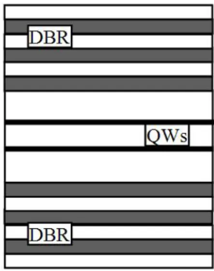
A typical inorganic semiconductor based microcavity (MC) is shown in Fig 1.2. The MC is composed of a planar Fabry-Perot cavity in which the high reflectivity mirrors are formed from ~10-20 repeats of distributed Bragg reflector quarter wavelength λ/4 layers. Quantum wells (QWs) are embedded within the cavity at the antinodes of the optical field to achieve maximum interaction between the QW excitons and the confined photon field. Both the exciton and photon states are confined, with the dispersion relations shown by the dashed lines in Fig 1.3.
The excitons and photons couple together to form new quasi-particles, cavity-polaritons which are part exciton, part photon. The existence of these new particles forms the basis of the new
Fig. 1.2- Schematic diagram of a semiconductor microcavity, showing quantum wells in the cavity region surrounded by high reflectivity (>99%) distributed Bragg reflector (DBR) mirrors.
6
phenomena and device structures. This is the regime of strong-coupling, and arises so long as the splitting between the two polariton branches is greater than the linewidths of the uncoupled modes. The splitting between the two polariton branches is given by the vacuum Rabi splitting, ΔVRS, and is determined by the exciton-photon interaction strength. The excitation oscillates back and forth between the two modes until the polariton decays by photon leakage through the Bragg mirrors and is converted to an external photon.
The polaritons have very small mass of order 10-4m
e as a result of the strong photon dispersion in the cavity (Fig. 1.3). This results in a density of states ~104 times smaller than that for excitons, a very important property which facilitates the achievement of state occupancies greater than one, the basis of the polariton laser.
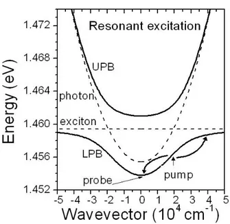
Fig. 1.3 - Dispersion of microcavity in strong coupling regime. Dashed – uncoupled exciton, cavity. Full - polariton coupled mode dispersion. LPB, UPB lower, upper polariton branches. Resonant excitation at the point of inflection leading to E and k-conserving pair scattering is indicated. The
7
The shape of the lower polariton dispersion curve is noteworthy (Fig. 1.3), with a point of inflection between k=0 and the uncoupled exciton energy. This permits new pair scattering processes (Fig 3) from the pump into signal and idler beams, in which energy and momentum are conserved (2Elaser=Esignal+Eidler, 2klaser=ksignal+kidler). Such pair processes are not achievable for the quadratic dispersions of either excitons or photons alone. Furthermore, the polaritons are directly accessible in reflectivity and emission, a key point for all the applications.
Polariton distributions can be probed directly along the dispersion curve by varying the external angle of the excitation beam, and populations can be injected at precise points in k-space, all features which do not arise in either bulk semiconductors or QWs.
The dispersion curves of Fig. 1.3 and Fig. 1.4 are controllable by design, by varying the number of quantum wells, the length of the cavity and the energy separation between the uncoupled modes (the detuning). This allows control of the depth of the ‘trap’ formed by the lower polariton branch (Fig. 1.3), and of the separation of the bottom of the trap from its 'environment' (the exciton reservoir), hence allowing loss processes to be minimised.
Fig.1. 4 - Polariton dispersion over large range of k (log scale), showing the exciton reservoir formed under non-resonant excitation conditions. The curved line indicates scattering out of the reservoir to
8
Both the exciton and photon components of polaritons are bosons, and hence the polaritons themselves have bosonic character. As a result they exhibit specific bosonic properties such as stimulated scattering and macroscopic state occupation (for fermions by contrast the state occupancy is restricted to one by the Pauli principle). The probability for a transition is proportional to (1+Nfinal), and since for bosons Nfinal may be >1, stimulation of transitions may occur. This is the origin of stimulated emission in conventional lasers, and stimulation of scattering between initial and final states depicted in Fig. 1.3 and Fig. 1.4.
Stimulation of scattering from klaser to k=0 in Fig. 1.3 or from the reservoir to k=0 in the polariton laser, leads to macroscopic occupation of the k=0 state.[8,9] The polaritons at k=0 convert to external photons by leakage through the Bragg mirrors and lead to the new form of coherent emission embodied in the polariton laser (Fig. 1.4).
Such a process is distinct from the stimulation in a photon laser since it is the polariton scattering process which is stimulated, as opposed to the photon emission in a laser. This separation of stimulation and emission leads to coherent emission without the requirement for population inversion, as in a photon laser, and hence to the prospect of very low threshold coherent emission.
In an equivalent description, the stimulation of scattering to k=0 leads to condensation of the polaritons to a state with macroscopic occupation from an incoherent exciton distribution. The achievement of polariton lasing is of major significance from the point of view of fundamental physics: a dynamical Bose condensate is formed in a process where symmetry is spontaneously broken from the incoherent reservoir to the coherent condensed state. Relative to Bose-condensates of atoms, the polariton condensate is composed of strongly interacting quasi-particles, has approximately 100 times higher density, is strongly coupled to the environment and importantly has a critical temperature greater than 300K, due to the very small polariton mass.
9
1.1.2 Microcavities as OPAs
In addition to the polariton laser application involving non-resonant carrier injection and stimulated scattering to the light emitting k = 0 state, the same or similar microcavities have considerable potential as very low threshold, micron size optical parametric amplifiers (OPAs). The principles of the OPA operation can be understood by reference to Fig. 1.3. In the presence of a pump beam at the point of inflection of the lower polariton dispersion, scattering of the pump polaritons to k=0 can be stimulated by a weak probe injected at k = 0.5 x 104 cm-1. Due to the very strong polariton interactions and the automatic phase matching between pump, signal and idler enabled by the unusual shape of the dispersion curve, very high ultrafast gains of the probe beam can be realised. Gains up to 10000 have been reported [5], with maximum temperature of operation of 200K in CdTe-based microcavities, the high temperature limit being determined by the relatively small exciton binding energy (20meV) in the CdTe quantum wells.
Compared to standard OPAs, the MC-based structures have micron size (as compared to mm-cm in conventional OPAs), gains up to 107cm-1 and orders of magnitude lower threshold (up to 106 times) due to the triple resonance condition evident on Fig. 1.3, and the large nonlinear coefficients of resonant semiconductor media. Such OPAs are inherently ultrafast because no energy is stored within the medium. They also have high potential as ultrafast switches. Since all the pump energy is split into signal and idler, they are very efficient in their redistribution of power in different directions.
1.1.3 The need for wide band gap materials
Many of the underpinning advances in polariton physics have been achieved in GaAs/AlGaAs based structures, and more recently in CdTe-based systems. In these materials due to the small
10
exciton binding energies (Ex) and small exciton oscillator strengths (f) the stimulated scattering phenomena are restricted to low temperatures (<50K) and to relatively low exciton densities. For example it was shown in [11] that in GaAs-based structures, due to the small exciton binding energies and oscillator strengths, exciton screening, loss of strong coupling and of the essential bosonic character occurs before the onset of polariton lasing.
For these reasons, one need to focus on GaN wide band gap materials where the large Ex and f provide the necessary electronic properties to enable polariton laser operation at both low and elevated temperatures and to achieve polariton-based optical parametric amplifier operation at 300K and above. The high oscillator strength enables large splittings between the polariton modes, and thus resistance to broadening effects which occur due to population of the exciton reservoir. The high exciton binding energy is also essential since the excitons in the quantum well will be stable at room temperature and highly resistant to screening. These two conditions provide the essential requirement to achieve polariton lasing, namely that the strong coupling between excitons and photons is retained under excitation conditions sufficient to achieve state occupancies greater than one and thus stimulated scattering to k=0 states.
As well as the obvious technological drive to achieve 300K operation, further advantages for polariton lasing arise from operation at higher temperature: at high temperatures the probability of energy and momentum conserving pair scattering from the reservoir into the trap increases strongly as a result of the wide spread in energy of the excitons, thus increasing strongly the probability of achieving condensation to k=0.
Wide band gap semiconductor materials, although efficient light emitters, have high thresholds for population inversion and lasing. Although GaN blue lasers are commercially available, they suffer from high threshold current (in the kA/cm2 range). This high J
th is to a large degree an intrinsic limitation due to the high carrier densities of states resulting from the high masses in wide band gap materials. The polariton laser offers a means to overcome this limitation: the polariton mass, and hence the density of states in the light emitting region, is 104 times smaller than that for
11
excitons, thus offering the prospect of very low threshold current, at least an order of magnitude less than in conventional “photon” lasers. Furthermore, the processes of stimulation and emission are separated in the polariton laser, as opposed to the situation in conventional VCSEL or edge emitting lasers, again leading to the prospect of very low threshold.
As well as promising low threshold coherent emission, the polariton laser is a generically new form of coherent light emitting device. It also offers intrinsically high modulation speeds and because of the low thresholds long lifetime and low power consumption. Such high performance green/blue/UV devices have potential to have a wide variety of applications in e.g. DVD writers/readers, projection tv, high definition printers.
1.1.4 Simulation software
The device simulators that are mostly used at present emerged during the ’80 (Silvaco [15]) and ‘90 (DESSIS of ISE-TCAD, acquired by Synopsis and now called Sentaurus Device [16]) and are based on a continuous media simulation approach. In particular, DESSIS is a multi-dimensional simulator for simulation of one, two and three-dimensional semiconductor devices and has mixed-mode capabilities for circuit simulation. Depending on the device which is simulated and on the accuracy which is needed different transport models can be used, which are drift-diffusion, self-heating, hydrodynamic, or Monte-Carlo. [17]
However all the available device simulators did not include models to describe exciton or polariton transport. Moreover, they needed improvements to handle GaN based device simulations, due to the particular properties of GaN wide band gap materials. Even the new device designs proposed on this work outlined the need of new simulation approaches or new refinements for the existing simulators.
12
For all these reasons, the work has been focused also on the developing of a new device simulator, called TiberCad, and on the improvement of Dessis to perform the optimization of the design of devices for the realization of polariton laser.
13
References
[1] M S Skolnick, T A Fisher and D M Whittaker, Semiconductor Science and Technology 13, 645, 1998
[2] M S Skolnick, A I Tartakovskii, R Butté, D M Whittaker and R M Stevenson, IEEE J Sel Top QE 8, 1060, 2002
[3] Special issue of Semiconductor Science and Technology, editors L Vina and J J Baumberg [4] F Tassoné, C Piermarocchi, V Savona, A Quattropani and P Schwendimann, Phys Rev B56, 7554, 1997, Phys Rev B59, 10830, 1999
[5] P G Savvidis, J J Baumberg, R M Stevenson, M S Skolnick, D M Whittaker, Phys Rev Lett 84, 1547, 2000
[6] R M Stevenson, V N Astratov, M S Skolnick, M Emam-Ismail, P G Savvidis, J J Baumberg, Phys Rev Lett 85, 3680, 2000
[7] R Houdré, C Weisbuch, R P Stanley, U Oesterle and M Ilegems, Phys Rev Lett 85, 2793, 2000
[8] A Imamoglu and R J Ram, Phys Lett, A214, 193, 1996
[9] Le Si Dang, D Heger, R André, F Boeuf and R Romestain, Phys Rev Lett 81, 3920, 1998 [10] M Saba, C Ciuti, J Bloch, V Thierry-Mieg, R André, Le Si Dang, S. Kundermann, A. Mura, G. Bongiovanni, J. L. Staehli, B. Deveaud, Nature 414, 731, 2001
[11] R Butté, G Delalleau, A I Tartakovskii, M S Skolnick, V N Astratov, J J Baumberg, G Malpuech, A Di Carlo, A V Kavokin, J S Roberts Phys Rev B65, 205310, 2002
14
[12] G Malpuech, A di Carlo, A V Kavokin, J J Baumberg, A Zamfirescu and P Lugli, Appl Phys Lett 81, 412, 2002
[13] G Malpuech, A V Kavokin, A Di Carlo and J J Baumberg, Phys Rev B65, 153310, 2002 [14] P G Lagoudakis, M D Martin, J J Baumberg, A Qarry, E Cohen, and L N Pfeiffer, Phys Rev Lett 90, 206401 (2003)
[15] Silvaco TCAD Solutions, http://www.silvaco.com.
[16] Synopsis Inc., http://www.synopsis.com.
[17] M.Auf Der Maur, A Multiscale Simulation Environment for Electronic and Optoelectronic Devices, PhD Thesis, Università di Roma Tor Vergata.
15
Chapter 2
Device simulation
The first part of the work has concerned the implementation of the exciton transport equations in TiberCad, the multiscale device simulator developed by the Optoelectronic Group at the Electronic Engineering Department of the University of Rome “Tor Vergata”.
At the same time, the improvement of the material parameter file of Dessis, a device simulation tool from Ise-TCad simulation software, has been carried out to create the requirement for the GaN based device simulation and to have a comparison from a commercial simulator and the in-house simulator TiberCad.
2.1 TiberCad
TiberCAD is a multiscale tool for the simulation of modern nanoelectronic and optoelectronic devices. Applications range goes from nanoelectronic to laser technologies including molecular electronics and bio-devices.
The TiberCAD project is aimed at the implementation of a device simulator which captures the most important physical concepts encountered in present and future electronic and optoelectronic devices. On the one hand the down-scaling of device dimensions requires the inclusion of more advanced quantum mechanical concepts which go beyond classical transport theories. On the other hand new devices are emerging whose functionality is based on properties not only related to electrons and holes but also to other quasi-particles in the system such as excitons, polaritons etc.
16
Often the active part of a device which needs a more elaborate and careful quantum-mechanical treatment is small compared to the overall simulation domain. The computational cost of the more accurate model, however, forbids its application to the whole domain. Moreover, in many systems, mechanical strain due to lattice mismatch or processing plays a crucial role for device performance and therefore needs an accurate description. Usually mechanical properties depend on a length scale that is much larger than the electrically active part of the device. This raises the need for a multiscale simulation environment capable of simulating different regions of a device using different physical models and coupling these simulations in a consistent way.
The models describing the different physical aspects encountered in modern devices are separated in TiberCAD into three families.
The first one contains the classical or semi-classical transport models for the quasi-particles in the system. These are based on drift-diffusion or hydrodynamical models, possibly with quantum corrections [1]. The drift-diffusion equations are written in terms of an adequate electro-chemical potential as shown for electrons in Eq. (2.1):
(
)
t
n
G
R
n
n n∂
∂
−
−
=
∇
∇
μ
φ
(2.1)where n, μn, R and G are the electro-chemical potential, the mobility, the recombination and the generation rate, respectively.
The second one comprises models for the description of mechanical strain induced by lattice mismatch or external forces. The current implementation is based on continuous elasticity theory, assuming crystallographically perfect heterointerfaces [2]. In this framework one solves a system of partial differential equations as given in Eq. (2.2):
0
2
1
0=
⎟
⎟
⎠
⎞
⎜
⎜
⎝
⎛
⎟⎟
⎠
⎞
⎜⎜
⎝
⎛
∂
∂
+
∂
∂
+
∂
∂
l k k l kl ijkl ix
u
x
u
C
x
ε
(2.2)17
where Cijkl, and ul are the elasticity moduli tensor, the lattice-matching abrupt strain induced by lattice mismatch and the deformation vector field, respectively. External mechanical forces can be applied by implying adequate boundary conditions, which allows the simulation of piezoelectric effects. The inclusion of atomistic models like valence force field is foreseen for the future.
The third class contains quantum-mechanical models for the calculation of electronic and optical properties of bulk materials and heterostructures. In this case a Schrödinger type equation has to be solved which leads to an eigenvalue problem. The hamiltonian for these models is calculated based on tight-binding and kp theories, including strain corrections in the usual ways [3]. An extension to account for quantum transport theories like non-equilibrium Green’s functions is under development.
The three sets of models are completed with the Poisson equation and with the models for material properties as e.g. mobility, recombination and generation processes or dependence of band gap on strain and doping. The different models are in general not independent from each other. Mechanical strain for example is an input for the quantum-mechanical calculation of the band properties of the materials, which in turn are needed for drift-diffusion simulations. A general iteration scheme for self-consistent coupling of different models will be implemented based on underrelaxation or predictor–corrector schemes [4]. Special care is needed if a model is not applied to the whole simulation domain. In this case the simulation results in the different regions have to be consistent on the common boundaries.
The partial differential equations occurring in the different models are discretized in the framework of the finite element method (FEM) and the box integration method.
All models are implemented for one, two and three space dimensions. This allows especially the simulation of 2D and 3D structures including realistic strain patterns, which is important for small structures.
18
TiberCAD is implemented in C++ using heavily the object-orientated features of the language. It is organized in a highly modularized way which allows for easy addition of new physical models and solvers. Every physical model is encapsulated in its own software module. The modules have a common interface so they can be handled in a model independent way by the control module of the simulator. Material parameters are stored in a database which is accessible to the different modules. The control module is responsible for the creation and setup of all the data structures and models and the flow control of the simulation.
TiberCAD relies on freely available software libraries which provide data structures and routines for the mesh handling for use with FEM [5] and environments for the numerical solution of the resulting (usually sparse) matrices [6] and [7].
2.1.1 The Exciton model in TiberCad
A model for exciton formation, dissociation and transport is proposed in the following for the simulation of electrically pumped polariton laser with a geometry similar to that of a VCSEL and resonant cavity LEDs. How the strain effects and the geometry of the device influence the exciton distribution for a GaN/InGaN laser structure have been demonstrated.
As already said, polariton laser offers intrinsically high modulation speeds, low thresholds, long lifetime and low power consumption. Gallium nitride is a material of choice for polariton lasers and room temperature operation is expected for laser structures based on this material [8].
In order to perform realistic simulations the 2D/3D TiberCAD software [9] has been used, extending it to include exciton formation and transport. Four equations are solved simultaneously, namely the Poisson equation, hole and electron transport at Drift-Diffusion level and the exciton transport equations. Exciton dynamics can be described by a simple Drift-Diffusion model [10,11]:
19 x
R
G
t
t
x
J
r
∇
−
−
=
∂
∂
(
,
)
(2.3)( )
r
( )
r
( )
r
j
drift,
t
=
−
μ
xx
,
t
∇
E
g (2.4)( )
r
( )
r
t
j
diff,
t
=
D
x∇
x
,
(2.5)where x is the exciton concentration, G is the generation term, R the recombination term, Eg is the band gap profile, Dx the exciton diffusion coefficient, μx the exciton mobility and Jx is the exciton current density. In our approximation, the generation term reads:
(
2)
in
np
G
=
γ
−
(2.6)and the recombination term can be described as:
rad non rad
x
R
−+
=
τ
τ
1
/
/
1
(2.7)where n and p are the electron and the hole concentrations, γ is the generation rate parameter, τrad and τnon-rad are the radiative and nonradiative recombination time constants.
The exciton system is treated in the model as the classical Boltzmann gas. Therefore, the exciton density is described as:
(
kT
)
N
x
=
xexp
−
ψ
x/
(2.8)with the density of states:
2 / 3 2 2 3 ⎟ ⎠ ⎞ ⎜ ⎝ ⎛ = h kT m N x x
π
(2.9)(mx is the exciton effective mass) and the chemical potential:
x x
−
E
=
φ
20
where φx is the effective exciton potential, which is analogous to the electro-chemical potential of electrons and holes, and Ex is the exciton energy, described as:
B
E
E
x=
g−
(2.11)where B is the exciton binding energy.
The exciton generation, recombination and dissociation time constants are obtained by Monte Carlo simulations which account for all the electron/hole/exciton scatterings in GaN [12]. In order to study the stationary case, the continuity equation for the effective exciton potential can be written as:
(
x
)
G
R
J
x=
−∇
x∇
x=
−
⋅
∇
μ
ψ
(2.12)The Eq. (2.12) is solved together with the stationary Drift-Diffusion equations for electrons and holes, using the Finite Element Method with proper boundary conditions, thus providing a self-consistently calculated potential profile.
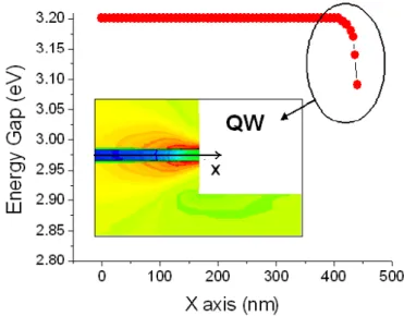
A GaN based diode structure with an embedded In0.14Ga0.86N quantum well as shown in Fig. 2.1 has been simulated. In Fig.2.2 the variation of the energy gap inside the quantum well and the εxx component of the strain are shown.
21
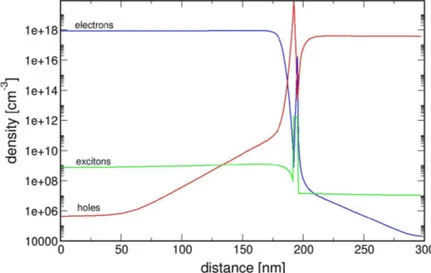
Results demonstrate a stronger lattice constant variation near the surface due to the strain relaxation at the free surface. The strain becomes less compressive moving toward the surface and this induce a decrease of the energy gap close to the surface. From the Eq. (2.3), one expects that the exciton current flow increases near the surface. In Fig. 2.3, it has been demonstrated that due to the inhomogeneous strain effects near the surface, the excitons are generated and also confined there. Generation of exciton in this region is also related to the electron/hole current which, for this device layout, is large near the laser diode surface. Finally in Fig. 2.4 the carrier densities are shown along the y-direction. As expected, the excitons are strongly confined inside the quantum well. For this polarization, the exciton density is about 1012 cm−3. From these simulations the conclusion is that an optimized device layout is required to focus the excitons to the cavity region which is typically at the center of the structure.
Fig. 2.2- Energy gap profile inside the quantum well (along x -direction). The strain (εxx
22
23
2.2 The simulation tool Dessis
Dessis is a multidimensional, electrothermal, mixed-mode device and circuit simulator for one-, two-one-, and three-dimensional semiconductor devices. It incorporates advanced physical models and robust numeric methods for the simulation of most types of semiconductor device ranging from very deep submicron Si MOSFETs to large bipolar power structures [13].
Dessis simulates numerically the electrical behavior of a single semiconductor device in isolation or several physical devices combined in a circuit. Terminal currents [A], voltages [V], and charges [C] are computed based on a set of physical device equations that describes the carrier distribution and conduction mechanisms.
Physical phenomena in semiconductor devices are very complicated and, depending on applications, are described by partial differential equations of different level of complexity.
Fig. 2.4- Electron, hole, and exciton density profile along a vertical section of the device.
24
Coefficients and boundary conditions of equations (such as mobility, generation–recombination rate, material-dependent parameters, interface and contact boundary conditions) can be very complicated and can depend on microscopic physics, the structure of the device, and the applied bias.
Dessis allows for arbitrary combinations of transport equations and physical models, which allows for the possibility to simulate all spectrums of semiconductor devices, from power devices to deep submicron devices and sophisticated heterostructures.
A real semiconductor device, such as a transistor, is represented in the simulator as a ‘virtual’ device whose physical properties are discretized onto a non-uniform ‘grid’ (or ‘mesh’) of nodes.
Therefore, a virtual device is an approximation of a real device. Continuous properties such as doping profiles are represented on a sparse mesh and, therefore, are only defined at a finite number of discrete points in space.
The doping at any point between nodes (or any physical quantity calculated by Dessis) can be obtained by interpolation. Each virtual device structure is described in the ISE TCAD tool suite by two files:
• The grid (or geometry) file contains a description of the various regions of the device, that is, boundaries, material types, and the locations of any electrical contacts. This file also contains the grid (the locations of all the discrete nodes and their connectivity). • The data (or doping) file contains the properties of the device, such as the doping
profiles, in the form of data associated with the discrete nodes. By default, a device simulated in 2D is assumed to have a ‘thickness’ in the third dimension of 1 μm. These features can be summarized as:
• An extensive set of models for device physics and effects in semiconductor devices (drift-diffusion, thermodynamic, and hydrodynamic models).
25
• General support for different device geometries (1D, 2D, 3D, and 2D cylindrical). • A extensive set of nonlinear solvers.
• A mixed-mode support of electrothermal netlists with mesh-based device models and SPICE circuit models.
Device structures can be created in various ways, including 1D, 2D, or 3D process simulation (DIOS), 3D process emulation (DEVISE), and 2D (MDRAW and DEVISE) or 3D (DIP and DEVISE) structure editors.
Dessis includes optional models for the comprehensive simulation of semiconductor lasers and lightemitting diodes (LEDs). Both edge-emitting lasers and vertical-cavity surface-emitting lasers (VCSELs) are supported. Drift-diffusion or hydrodynamic transport equations for the carriers, the Schrödinger equation for quantum well gain, modal optical rate equations, and the Helmholtz equation are solved self-consistently in the quasistationary and transient modes.
Spontaneous and stimulated optical recombinations are calculated in the active and bulk regions according to Fermi’s golden rule. They are added as carrier recombination mechanisms in the continuity equations and as modal gain and spontaneous emission in the photon rate equations. Different line-width broadening models are available for gain broadening.
Both bulk and quantum well (QW) lasers can be simulated. In the case of QW lasers, the optical polarization dependence of the optical matrix element is automatically taken into account. The QW subbands are calculated as the solution of the single-band Schrödinger equation in the effective mass approximation, assuming a box-shaped potential or by a multiple-bands kp method. Strain effects can also be taken into account. The distribution of carriers in the well is determined according to the quantum mechanical wavefunctions and QW density of states.
In the unquantized direction, drift-diffusion transport applies to the carriers. In the quantized direction, two transport models are available. The simple transport model assumes thermionic
26
emission at the heterointerfaces, which form the quantum well. The advanced transport model separates the QW carrier distributions into a bound and continuum distribution. The fraction of bound and continuum carriers is then self-consistently computed by additional scattering equations, mainly contributed by carrier-carrier and carrier-optical phonon scatterings.
2.2.1 Upgrading of Dessis material parameter file
Gallium nitride and related nitrides are quite new for simulation tools. Even thought several real application have been already achieved with GaN [14], identification of correct material parameters is still under debate. For this reason, the material parameter file of Dessis was improved by direct comparison with available experimental data. This part of the work was made in the collaboration of the group from EPFL of Lausanne. The information used for the upgrading of the file come from Refs. [15-17]. Here, the parameters for nitrogen-containing semiconductors have been studied and described (Fig. 2.5). In Appendix A and B, a complete description of the new material parameter file is reported.
27
28
References
[1] M.G. Ancona and G.J. Iafrate, Quantum correction to the equation of state of an electron gas in a semiconductor, Phys. Rev. B. Condens. Matter 39 (1989), p. 9536
[2] M. Povolotskyi and A.D. Carlo, Elasticity theory of pseudomorphic heterostructures grown on substrates of arbitrary thickness, J. Appl. Phys. 100 (2006), p. 063514
[3] S.L. Chuang and C. Chang, View the MathML source method for strained wurtzite semiconductors, Phys. Rev. B 54 (1996), p. 2491.
[4] A. Trellakis, A.T. Galick, A. Pancelli and U. Ravaioli, Iteration scheme for the solution of the two-dimensional Schrödinger–Poisson equations in quantum structures, J. Appl. Phys. 81 (1997), p. 7880
[5] B.S. Kirk, J.W. Peterson, libMesh library, http://libmesh.sourceforge.org.
[6] S. Balay, K. Buschelmann, W.D. Gropp, D. Kaushik, M.G. Knepley, L.C. McInnes, B.F. Smith, H. Zhang, PETSc Web page. http://www.mcs.anl.gov/petsc, 2001.
[7] V. Hernandez, J.E. Roman, V. Vidal, SLEPc Web page. http://www.grycap.upv.es/slepc. [8] G. Malpuech et al. App. Phys. Lett. 81,412 (2002).
[9] www.tibercad.org
[10] Tamor M.A. and Wolfe J.P. 1980, Phys.Rev.Lett44 1703; [11] V Emiliani, et al. J. Phys.: Condens. Matter 11 (1999) 58895900. [12] G. Kokolakis et al. Phys. Stat. Sol. (a) 195, 618 (2003)
29
[13] Dessis Manual, ISE Integrated Systems Engineering, Release 9.5
[14] Merfeld D. W. et al., Influence of GaN Material Characteristics on Device Performance for Blue and Ultraviolet Light-Emitting Diodes, Journal of Electronic Materials, Nov 2004
[15] Vurgaftman I. and Meyer J. R., Band parameters for nitrogen-containing semiconductors, J. Appl. Phys., Vol. 94, No. 6, 15 September 2003
[16] Chris G. Van de Walle and Jorg Neugebauer, Small valence-band offsets at GaN/InGaN heterojunctions, Appl. Phys. Lett. 70(19), 12 May 1997
30
Chapter 3
Design and optimization of GaN based LED and Polariton
Laser / VCSEL
The second part of the work concerned the study of new structures and devices to optimize the design of the polariton laser.
The first step was to compare experimental data and simulation results of simple LED structures in order to validate the simulation tool performances. Then, several designs of LED structure have been simulated to understand the influence of the geometrical parameters and the material properties on the characteristics of the device. As a consequence, new VCSEL structures have been designed, optimizing the electrical injection.
These results led to publication of papers and a patent, as described in the next chapter.
3.1 Influence of mesa contact dimension on the GaN/InGaN LED
properties
As previously shown, the basic geometry of electrically driven polariton lasers is very similar to that of vertical cavity surface emitting lasers (VCSELs) and resonant cavity light-emitting diodes (RCLEDs). For this reason, a simple GaN-based LED geometry has been intentionally adopted in order to better understand the factors affecting the LED characteristics (Fig. 3.1). Using this geometry, devices with several p-contact and mesas diameters have been studied.
31
Starting from standard LED structures grown in LASPE laboratories of EPFL (Lausanne, Switzerland), experimental studies and simulations of GaN-based LED structures have been done in order to highlight and to confirm the factors influencing the devices performances and to improve the software simulations. Several parameters are used to evaluate the emission characteristics of a LED structure. The quantum efficiency, together with the I-V characteristics, will be used as quality parameters. A simple LED geometry has been intentionally adopted in order to better understand the factors affecting the LED characteristics.
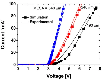
The LED structures studied are grown by MOVPE on 2 inch sapphire substrates. The typical geometry of the device consists of: 2 μm Si doped (3×1018 cm-3) n-GaN layer; 3 x QWs [12 nm Si doped GaN; 1.5 nm In0.14Ga0.86N]; 20nm Al0.2Ga0.8N electron-barrier; 120 nm Mg doped (~3×1017 cm-3) p-GaN layer. For this geometry, the device has been studied with three different MESAs diameters (540 μm, 240 μm, 190 μm) P-type contacts are realized using a Ni/Au metallization on top of the MESA structures with a diameter 140μm smaller than the MESA diameter (Fig. 3.1). For this LED with 3 QWs a central emission wavelength λ = 403 nm is measured. Device with similar structure but different number of quantum well have been also fabricated in order to compare with the 3QW reference structure.
32
Devices are simulated using the IseTCad simulation software. Here, Poisson equation, carrier continuity equations for electrons and holes, and transport equations at drift-diffusion level are solved in a self-consistent fashion. Full account of spontaneous and polarization field is considered. Material parameters used in the simulation are tuned according the experimental data previous reported by EPFL [1-3] and described in the previous chapter.
The setup used for the characterization of the device made in LASPE laboratories consists of a probe station, a large area silicon photodiode (Hamamatsu S1337-1010BR) and a HP 4145A semiconductor parameter analyzer used as DC voltage source, current and photocurrent monitor. The devices are in direct contact with the surface of the detector and the emitted light is collected from the backside of the substrate.
The IV characteristics of LED having different contact and MESA size as a function of the injection current is shown in Fig. 3.2 where both experimental and simulation results have been compared. 0 1 2 3 4 5 6 7 8 0 20 40 60 80 100 190 μm 240 μm MESA = 540 μm
Cu
rr
en
t [mA]
Voltage [V]
Simulation ExperimentalFig. 3.2 - Current-voltage (IV) characteristics of the fabricated LEDs for several MESA diameters. Comparison between simulation results and experimental data.
33
A very good comparison between experiment and simulation is achieved (in the simulation nominal parameter are considered). This shows the very good control and reproducibility of material parameters in the fabrication process.
External quantum efficiency (ηext) of InGaN/GaN based LEDs has been shown to increase by increasing the number of QWs in the active region [4]. Samples having one, three and five QWs have been fabricated, characterized and simulated in order to find an upper limit for the number of QWs which optimizes the ηext. Simulations have been performed by varying the numbers of QWs in the 50μm mesa diameter device. The internal quantum efficiency, ηi as the ratio between the radiative recombination rate in the QWs and the total recombination rate have been calculated. ηi is related to the external quantum efficiency ηext by the equation:
extract i inj ext
γ
η
η
η
=
⋅
⋅
(3.1)where γi is the injection efficiency and ηextract is the extraction efficiency. In the following, the simplifying assumption that both γi and ηextract are independent on the number of quantum wells have been done. Fig. 3.3, shows the calculated internal quantum efficiency as well as the measured external quantum efficiency, both normalized to the maximum efficiency value obtained for the device with one quantum well. A qualitative agreement between simulation results and experimental data is achieved. The efficiency increases by using a larger number of quantum wells. This is due to the more strict dependence of radiative recombination rate (RR) on the quantum well number with respect to the sum of RR and the non-radiative recombination rate (RNR). In fact, the contribution to the RR arises from the QWs while the RNR is the sum of the bulk and QW contributions, RNR=RNR(bulk)+RNR(QWs). Saturation of quantum efficiencies for both experimental and simulation results, is achieved for samples where the number of QWs is equal or larger than three. By increasing the number of quantum well, RNR(QWs) becomes much larger that RNR(bulk) which results in a saturation of the efficiency.
34
The difference in ηext is even more dramatic in the low injection range, where ηext for devices with 5 QW is more than 2 orders of magnitude higher than for samples with only 1 QW. In the
Fig.3.3 - Simulated Internal Quantum Efficiency for devices with a different number of quantum wells.
Fig.3.4 - Experimental External Quantum Efficiency (EQE) for devices with a different number of quantum wells.
35
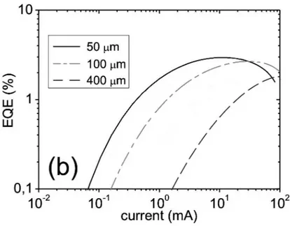
realized devices, the presence of non radiative channels (i.e. dislocations, point defects, etc.) bypassing the active region, is responsible for the decreasing of ηext in the low current range. Having a defect free structure would imply a constant ηext independently of the injection current. For this reason, considering a constant superficial defect density, when the device size is decreased (higher current density for the same current value), the ηext curves shift toward lower injection current values as shown in Fig. 3.5.It can be also observed that, as the contact size is decreased, the maximum EQE increases. This value, for devices having a 50 μm contact diameter, is almost two times higher than for devices having a 400 μm contact diameter. This result could be explained by considering an improved light extraction near the MESA edges.
In fact, light extracted from LEDs is the sum of the light extracted directly from the substrate and of a small fraction of light extracted from the device sidewalls that reaches the bottom side of the substrate. Other phenomena, like photon re-absorption into the QWs as well as photon recycling, affect the overall efficiency of the devices. Absorption in the n-GaN and p-GaN regions can be neglected for the propagation direction perpendicular to the emitting surface, since the
36
device thickness (~3 µm) is much smaller than the absorption length at 400 nm (100 to 500 cm-1) [5].
The simulation results of Fig. 3.6 show that the radiative recombination between holes and electrons mainly occurs into the first QW close to the AlGaN barrier. This is due to low hole mobility (20 cm2V-1s-1) with respect to the electron one (1500 cm2V-1s-1) and to the presence of an AlGaN e-blocking layer.
3.2 Design of current confinement layer
In order to optimize the current confinement in the center part of the device, three different structure have been simulated. As shown in Fig. 3.7, the first design has the AlInN current confinement layer below the active region, with the aim of forcing the carrier transport in the center part of the device (as shown in Ref. [6]); the second design has a double confinement layer; the
Fig. 3.6 - Radiative recombination rate [cm-3s-1] inside the quantum wells (x-direction) at 5V
37
third one a single layer above the active region. The Internal Quantum Efficiencies (IQE) (Fig. 3.8), the Focusing Efficiencies (Fig. 3.9) (defined as the ration between the total radiative recombination rate of the QWs in the aperture region and the total recombination rate of the QWs in the whole device) and the IV characteristics (Fig. 3.10) of these three structures have been investigated.
Fig. 3.8 - Internal quantum efficiencies for three different design of the AlInN current confinement layer
38
As shown, the focusing efficiency increases by using the top layer and the double layer. But the the current is strongly reduced. For these reasons, the structure with the bottom AlInN layer has been chosen as the best trade off of the characteristics studied in these simulations.
However, the AlInN layer is not enough to confine the current in the center part of the device: when the applied voltage increases, a spread of the current has been observed in the device (fig. 3.11). [18] This behavior has been confirmed also by simulations. As shown in fig. 3.12, the maximum value of the radiative recombination rate is quite focused in the center part of the device
Fig. 3.10 - IV characteristics for three different design of the AlInN current confinement layer Fig. 3.9 - Focusing efficiencies for three different design of the AlInN current confinement layer.
39
for 3V applied, but when the voltage increases, radiative recombination rate spreads towards the p contact region. This behavior will be better described and explained in the next paragraphs.
Fig. 3.12 – Radiative recombination rate map in the half part of the device (in x=0 is the symmetry axis for cylindrical symmetry) at 3V and 8V applied.
Fig. 3.11 - EL intensity maps of a GaN based LED with AlInN layer confinement realized at EPFL laboratories, at (a) 200 nA, (b) 1 μA, (c) 50 μA, and (d) 1 mA injection currents.
40
3.3 The influence of mobility unbalance
Concerning the enhancement of electrical and optical coupling properties of POLARITON laser (PLASER) and VCSEL structures, one of the main problems remains the focusing of the carrier density in the central part of the device where optical mode confinement is present. For this reason the use of an efficient current confinement layer is required even though this has been shown to be limited to low applied voltages.[6] The main effect of the reduce carrier focusing efficiency is the excitation of unwanted higher order modes strongly raising the lasing threshold to an unacceptable level. [7]
So far, the presence of strong polarization field [8] and the large resitivity of the p-layers forming the structure [7, 9] have been advocated to explain the non-uniform charge injection which reduces the carrier focussing efficiency and the consequent failure in the realization of electrically driven VCSEL and PLASER. In fact, as will be showed, this effect is mainly related to the strong unbalance between electron and hole mobilities.
The simulated structure is similar to the one developed in [6]. A schematic layout of simulated device is shown in Fig. 3.13: the mesa diameter is 20 μm, contacts are rings with inner/outer diameters of 10.5/18 μm for the p-contact and 33.25/52.25 μm for the n-contact, the current confinement is achieved by selective oxidation of an Al0.82InN layer of 25 nm high, leaving an horizontal aperture of 5 μm. The structure has the following layer sequence: 85nm p-doped (3x1019cm-3) Al0.15GaN, 10nm p-doped (3x1019cm-3) Al0.20GaN electron barrier layer, 3x GaN/Al0.15GaN (2nm/3nm) QWs forming the active region, 25 nm partially oxidized Al0.82InN layer, 140 nm n-doped (3x1018cm-3) Al
41
Material parameters used in the simulations have been tuned according the experimental data presented in Refs.[1][2][11]. We have considered a realistic field dependent mobility model [13]:
( )
β β μ μ μ 1 0 0 1 ⎥ ⎥ ⎦ ⎤ ⎢ ⎢ ⎣ ⎡ ⎟⎟ ⎠ ⎞ ⎜⎜ ⎝ ⎛ + = sat v E E (3.2)where μ0 denotes the low field mobility, E the driving field, νsat the saturation velocity and β is the Caughey-Thomas parameter [14].
The low field mobilities are equal to μoe=1100cm2/Vs for electrons [14] and μoh=20 cm2/Vs for holes [15].In the simulations, the Bragg reflectors have been not considered since the attention has been focused only on charge injection mechanisms.
As clearly shown by the 2D maps of Fig 3.14a, the radiative recombination rate, which is proportional to the local product of electron and hole densities, is not focussed in the central region of the VCSEL where the intensity of the electromagnetic field is high. This characteristic is not related to the choice of the thickness and doping of the different layers forming the structure. In
Fig. 3.13 - Schematic section of the simulated device (cylindrical symmetry has been used in simulation)s. The dashed line represent the symmetry axis.
42
fact, additional simulations have been performed to equalize the p and n layers resistances [7] but also in this case the radiative recombination rate is not focussed in the central part of the VCSEL.
The main motivation for the lost of carrier injection focussing is the strong unbalance of the electron and hole mobilities. Electrons injected in the QWs experience a larger drift (vdrift=μE) compared to the holes injected by the p-contact and consequently the recombination between electron and hole occurs far apart from the center of the device toward the p-contact region. One should consider that in the active region the electric field along the y-axis reaches values of the order of kV/cm.
To prove this assertion several simulations have been performed where a perfectly balanced electron and hole mobility, both equal to 1100 cm2/Vs, is considered. The calculated 2D radiative recombination rate map is shown in Fig. 3.14b. In this case, a stronger focusing of the recombination rate in the central zone of the quantum wells is shown. To be noticed that this conclusion is not related to particular choice of the mobility value but only to the balance between electron and hole mobilitites.
Fig. 3.14 - Recombination maps (cm−3 s−1) for the VCSEL at 7 V around the active region. (a) Simulation result with real mobility values μoc=1100 cm2 /V s, μoh=20 cm2 /V s and (b) simulation
43
In fig. 3.15 the radiative recombination rate and the absolute value of the current density for both balanced and unbalanced mobility case along the horizontal x-direction for the central quantum well have been reported. The focusing effect induced by the balancing of the mobility is quite evident. However, focusing induced by mobility balance is only related to the radiative recombination and not to the current density. In fact, current density peaks in the region of high velocity (i.e. high electric field) independently of the mobility value. This shows how the optimization procedures for current injection in GaN-VCSEL (or PLASER) should concentrate directly on carrier focusing without pursuing the focusing of the current which is related to both densities and velocities.
In order to describe quantitatively the focussing properties of the structure and the relation with the mobility, the focussing efficiency (FE) has been extracted from the simulation. Moreover, the internal quantum efficiency (IQE) as the ration between the total radiative recombination rate in the QWs and the total recombination rate in the structure (obtained summing the radiative and non-radiative recombination rates) has been calculated.
Fig. 3.15 - Radiative recombination rate and absolute value of the current density for both balanced and unbalanced mobility case in the middle quantum well along the horizontal x direction.
44
The calculated FEs for both real unbalanced mobility model and perfectly balanced mobility model as a function of the applied potential are shown in Fig 3.16. Above threshold (Vth~3 V) the focussing efficiency is much larger in the balanced mobility simulation than in the real unbalanced mobility condition. Almost the 60% radiative recombination occurs in the aperture region of the QW when electrons and holes have the same mobility. This reduce to 20% when a the realistic unbalanced model for the mobility is considered. As discussed above, these results do not depend on the mobility value used for the mobility balanced simulations and are not related to the presence of heterointerfaces between GaN/AlGaN forming the QWs. In fact, the same conclusion holds for a VCSEL with bulk GaN active region. The internal quantum efficiency, on the other hand, is not influenced by the mobility balance (fig.3.16).
Several design strategies could be considered for contrasting the reduce focussing efficiency induced by the electron and hole mobility unbalance, as a proper strain engineering of the layers to improve hole mobility or considering an inverted structure, where the n-doped part of the device is growth on the p-doped layers.
Fig. 3.16 - FE and IQE for the VCSEL. Results are reported for real mobility values and for the case where electron mobility=hole mobility=1100 cm2 V s.
45
3.4 Enhancement of carrier focusing
The relation between the focusing efficiency and the unbalance between electron and hole mobility have been outlined in the previous section. To overcomes the focusing limitation of conventional GaN based VCSELs and PLASERs a new device structure is proposed where the n-layer is on the top of the p-n-layer .
The schematic layouts of the simulated structures are shown in Fig.3.17. Here a conventional structure (Fig. 3.17a), similar to the device described before where the p-doped layer is on top of the n-doped layer, and a new “inverted” structure (Fig. 3.17b) where the n-layer is on top of p-layer are proposed. For both structures the mesa diameter is 20 μm, upper contacts are rings with inner/outer diameters of 10.5/18 μm and 33.25/52.25 μm for the other contact, the current confinement is achieved by selective oxidation of an Al0.82InN layer of 25 nm high, leaving an horizontal aperture of 6 μm [16]. The conventional structure (fig. 17.a) has the following layer sequence: 85nm p-doped (3x1019cm-3) Al
0.15GaN, 10nm p-doped (3x1019cm-3) Al0.20GaN electron barrier layer, 3x GaN/Al0.15GaN (2nm/3nm) QWs forming the active region, 25 nm partially oxidized Al0.82InN layer, ~140 nm n-doped (3x1018cm-3) Al0.15GaN.
The “inverted” structure (fig. 17.b) has 71 n-doped (3x1018cm-3) Al
0.15GaN, 25 nm partially oxidized Al0.82InN layer, 3x GaN/Al0.15GaN (2nm/3nm) QWs forming the active region, 10nm p-doped (3x1019cm-3) Al
0.20GaN electron barrier layer, 125nm p-doped (3x1019cm-3) Al0.15GaN. Only few realization of such inverted structure [16] have been reported even though the relation with focusing efficiency has never been outlined.
46
Fig. 3.18 shows the radiative recombination rate, which is proportional to the local product of electron and hole densities, in the middle QW along the horizontal direction (here the x-axis origin is the centre of the device). One can observe that for the conventional device the radiative
Fig. 3.18 - Radiative recombination rate for the conventional and inverted structure in the middle QW along the horizontal direction. The origin of the X axis is the centre of the device. Results are
obtained for an applied potential of 5 V.
47
recombination is not focussed in the central region of the VCSEL where the intensity of the electromagnetic field is high.
In order to describe quantitatively the focusing properties of the structure, we extract from the simulation a focusing efficiency (FE). The FE for the conventional structure (Fig. 3.19) is quite low and it is below 20% in typical operative conditions. As said, the main reason for this low FE is the unbalance between electron and hole mobilites, which is quite large in GaN related semiconductors.
As shown in the radiative recombination rate of Fig 3.18 and in the focusing efficiency plotted in Fig. 3.19, the inverted structure allows for a better confining of electron and holes in the current aperture region resulting in a strong improvement of the focusing efficiency which reaches an average value of 60% in the operative region with a peak of 80% in the region close to the threshold (the typical operative region for PLASERs). Fig. 3.19 shows also the internal quantum efficiency (IQE).
Fig. 3.19 - Focusing efficiency and Internal Quantum efficiency for the conventional and inverted structure as a function of the applied potential.
![Fig. 3.6 - Radiative recombination rate [cm -3 s -1 ] inside the quantum wells (x-direction) at 5V applied](https://thumb-eu.123doks.com/thumbv2/123dokorg/8050090.123176/43.892.184.758.205.552/fig-radiative-recombination-inside-quantum-wells-direction-applied.webp)