Alma Mater Studiorum - Universit`a di Bologna
DOTTORATO DI RICERCA IN
INGEGNERIA ELETTRONICA, INFORMATICA
E DELLE TELECOMUNICAZIONI
Ciclo XXIV
Settore Concorsuale di afferenza: 09/E3 ELETTRONICA
Settore Scientifico-disciplinare: ING-INF/01 ELETTRONICA
NUMERICAL MODELLING OF
GRAPHENE NANORIBBON-FETS
FOR ANALOG AND DIGITAL APPLICATIONS
Presentata da: Ilaria Imperiale
Coordinatore Dottorato:
Relatore:
Chiar.mo Prof. Ing.
Chiar.mo Prof. Ing.
Luca Benini
Massimo Rudan
Sommario
Il grafene, uno strato monodimensionale di atomi di carbonio disposti a nido d’ape, `e stato recentemente isolato a partire dalla grafite. Questo ma-teriale dispone di propriet`a fisiche molto interessanti, tra cui eccellenti mo-bilit`a elettroniche, capacit`a di trasporto di corrente e conduttivit`a termica. Inoltre, i portatori si muovono all’interno del grafene in condizioni quasi balistiche, e la sua struttura planare ed il suo spessore pari ad uno strato atomico fanno supporre che transistor ad effetto di campo (field-effect transistors, FETs) che utilizzano il grafene come materiale di canale sareb-bero poco condizionati dagli effetti di canale corto, e che l’integrazione e lo scaling del grafene sarebbero pi `u semplici di quelli di altri materiali emergenti per le applicazioni post-CMOS. In considerazione di questo, il grafene negli ultimi tempi `e stato oggetto di grande studio, come poten-ziale candidato per l’utilizzo in dispositivi su scala nanometrica per ap-plicazioni elettroniche. Il maggiore limite per l’utilizzo del grafene nei dispositivi elettronici `e il fatto che `e un semi-metallo, ossia non dispone di un gap energetico. La presenza di un gap energetico `e essenziale nei tran-sistor digitali, che necessitano di un gap per chiudere il canale conduttivo quando il dispositivo `e nello stato di OFF. In questa tesi sono stati studiati i graphene nanoribbons (GNRs), che sono delle sottili strisce di grafene, nei quali un gap energetico `e causato dal confinamento quantistico delle cariche nella direzione trasversale.
Dato che i GNR-FETs realizzati sperimentalmente sono ancora lontani dallo essere ideali, essenzialmente per l’eccessiva larghezza e per la rugosit`a ai bordi, una descrizione accurata dei fenomeni fisici presenti in questi dispositivi `e necessaria per fare valutazioni corrette riguardo alla perfor-mance di queste nuove strutture. Con questo fine, un codice `e stato svilup-pato e utilizzato per studiare la performance di GNR-FETs di larghezza da 1 a 15 nm. Data l’importanza di una descrizione accurata degli effetti quantistici nel funzionamento dei dispositivi in grafene, `e stato utilizzato un modello di trasporto completamente quantistico: la dinamica degli elettroni `e stata descritta attraverso un modello di Hamiltoniano tight-binding (TB) e il trasporto `e stato risolto con il formalismo delle funzioni di non equilibrio di Green (NEGF). Sono stati considerati sia il trasporto
di tipo balistico che dissipativo. L’interazione elettrone-fonone `e stata in-clusa nell’approssimazione auto-consistente di Born.
In considerazione della diversa ampiezza del gap energetico di cui dispon-gono, i GNR stretti sono potenziali candidati per le applicazioni digitali, mentre quelli di larghezza maggiore per le applicazioni a radiofrequenza.
Abstract
Graphene, that is a monolayer of carbon atoms arranged in a honeycomb lattice, has been isolated only recently from graphite. This material shows very attractive physical properties, like superior carrier mobility, current carrying capability and thermal conductivity. In addition, the carriers move inside graphene in quasi-ballistic conditions and its planar structure and atomic thickness suggest that field-effect transistors (FETs) made of graphene as channel material would be slightly affected by short-channel effects and its integration and scaling could be easier than that of other emerging material for post-CMOS applications. In consideration of that, graphene has been the object of large investigation as a promising candi-date to be used in nanometer-scale devices for electronic applications. The main disadvantage for the application of graphene in electronic devices is the fact that it is a semi-metal, namely it does not show any energy band-gap. The presence of a band-gap is essential in digital transistors, that require a band-gap to close the conductive channel when the device is in the OFF state. In this work, graphene nanoribbons (GNRs), that are nar-row strips of graphene, for which a band-gap is induced by the quantum confinement of carriers in the transverse direction, have been studied. As experimental GNR-FETs are still far from being ideal, mainly due to the large width and edge roughness, an accurate description of the phys-ical phenomena occurring in these devices is required to have valuable predictions about the performance of these novel structures. A code has been developed to this purpose and used to investigate the performance of 1 to 15-nm wide GNR-FETs. Due to the importance of an accurate de-scription of the quantum effects in the operation of graphene devices, a full-quantum transport model has been adopted: the electron dynamics has been described by a tight-binding (TB) Hamiltonian model and trans-port has been solved within the formalism of the non-equilibrium Green’s functions (NEGF). Both ballistic and dissipative transport are considered. The inclusion of the electron-phonon interaction has been taken into ac-count in the self-consistent Born approximation.
In consideration of their different energy band-gap, narrow GNRs are ex-pected to be suitable for logic applications, while wider ones could be
Contents
Introduction 1
1 Model 7
1.1 Overview of the model . . . 8
1.2 Inclusion of electron-phonon interaction . . . 13
1.2.1 Acoustic phonon scattering . . . 14
1.2.2 Optical phonon scattering . . . 17
1.3 Self-consistency of potential solution . . . 20
1.4 Summary . . . 20
2 GNR-FETs for digital applications 21 2.1 Simulated structure . . . 22
2.2 Effect of acoustic phonons . . . 22
2.3 Effect of edge roughness . . . 27
2.4 Summary . . . 32
3 GNR-FETs for analog applications 33 3.1 Performance evaluation . . . 34
3.2 Design considerations . . . 37
3.2.1 Asymmetrical doping . . . 37
3.2.2 Use of high-k oxide . . . 40
3.2.3 Introduction of underlap region . . . 42
3.3 Extension to GNR-FETs with metal contacts . . . 43
3.3.1 Optimization criteria . . . 45
3.4 Generalization of the study . . . 50
3.5 Summary . . . 62
Conclusions 65
Bibliography 67
Introduction
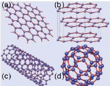
Current integrated-circuit (IC) technology is driven by the silicon transis-tor, or more importantly, the ability to increasingly scale down the tran-sistor size in order to enhance the performance of an individual transis-tor while also increasing the total number of transistransis-tors for a given area. However, as feature sizes of silicon transistors approach the nanometer scale, transistor performance no longer scales in proportion with device dimensions, particularly channel length [1]. In recent years, the request for increasing performance and reducing area occupancy for both active and passive electronic components has pushed the scaling process ev-ery day closer to the physical limits of the silicon-based MOS technol-ogy. Thus, the research has been oriented towards the investigation of new nanoscale devices capable to overcome the main limitations observed for silicon MOSFETs at the nanometer scale, like short channel effects (SCEs) and gate leakage. In particular, both the introduction of new architectures and new channel materials have been proposed. Among those, carbon-based materials like graphene and carbon nanotubes have attracted large interest in the scientific community, due to their fascinating electrical prop-erties. Graphene is a monolayer crystal of carbon atoms arranged in a hexagonal structure of carbon atoms arranged in a honeycomb lattice. It is the fundamental building block of graphitic materials, and thus is im-portant in determining the electronic properties of other carbon allotropes such as graphite (3-D stack of graphene sheets), carbon nanotubes (1-D rolled up graphene cylinder), and fullerenes (0-D molecules of wrapped-up graphene with the introduction of pentagons), shown in fig. 1. In fact, graphite can be viewed as a stack of weakly bonded graphene layers and carbon nanotubes (CNTs) can be considered as resulting from the folding of a graphene sheet to a cylinder. Although graphene properties have been known for a long time, only in 2004 a research group at Manchester Uni-versity succeded in isolating graphene from graphite [2]. The employed technique was based on a repetitive exfoliation of a graphitic block using adhesive tape and the subsequent deposition of the flakes onto an oxi-dized silicon wafer. Although it was not obtained a perfect single layer of graphene, that was the first reported experiment in which graphene
Figure 1:Allotropes of carbon include: a) graphene, b) graphite, c) CNTs and d) fullerenes.
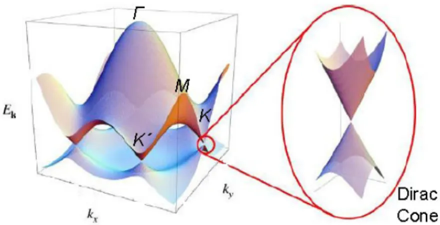
layers had been isolated. Since then, the fabrication of graphene has sig-nificantly improved and rapid advancements have been achieved in the understanding of the physical mechanisms typical of this material. The excellent electrical and thermal properties of graphene hold great promise for applications in future IC technology [3]. The interesting properties of graphene arise from its two-dimensional structure that confines electrons in one atomic layer and that causes charge carriers to behave as mass-less Dirac fermions [4, 5] and to its low density of states (DOS) near the Dirac point, which causes the Fermi energy to shift significantly with vari-ation of carrier density [6]. Early measurements suggested graphene has high intrinsic mobility (≈ 40000 cm2/Vs) [7] and high thermal conductiv-ity (≈ 600 W/m K) [8], both significantly greater than in silicon and other standard semiconductors. Therefore, graphene has attracted large atten-tion as a promising candidate for future electronics, with specific interest for radiofrequency applications. A graphene transistor fabricated from graphene epitaxially formed on a SiC wafer has demonstrated a cutoff fre-quency as high as 100 GHz [9]. In addition, optical properties of graphene make it a promising material for IR optoelectronics [6] and its high elec-trical and thermical conductivity, makes it an attractive material for fu-ture high-speed interconnects. The main drawback for the application of graphene in electronic devices is the fact that it is a semi-metal, namely it does not present an energy band-gap, as shown in 2. The presence of a band-gap is essential in digital transistors, that require a band-gap to close the conductive channel when the device is in the OFF state. Therefore, the lack of a band gap results in very poor ION/IOF F ratio, too low to be used
Figure 2:Band structure of graphene showing six Dirac (K and K) points and a linear dispersion relationship around them. Image taken from [11].
in digital logic [10]. Recently, several ways have been proposed in the lit-erature to create a band gap in graphene. One of the most interesting tech-niques is patterning graphene into narrow ribbons, so that the carriers are confined in a quasi 1-dimensional layer, this resulting in the opening of an energy band-gap. With respect to carbon nanotube field-effect transistors (CNT-FETs), FETs that use graphene nanoribbons as the channel material (GNR-FETs) exhibit comparable performance, reduced sensitivity on the variability of channel chirality, and similar leakage problems due to band-to-band tunneling [12]. However, as carbon nanotubes [13, 14], graphene nanoribbons can be either seminconducting or metallic. A sketch of the two main edge orientations are depicted in fig.3. Zigzag GNRs are metal-lic, while armchair can be either semiconducting or metalmetal-lic, depending on the number of atoms in the lateral cross-section. This property is very attractive, since it could lead to the introduction of a fully carbon-based tecnology, where both the active devices and interconnects could be made of the same material, thus avoiding technology compatibility issues. As far as the energy band-gap width is concerned, large theoretical and ex-perimental work has been carried out in recent years to investigate the energy band-gap engineering in graphene nanostructures. For example, in [16], from the analysis of experimental data carried out by the research group guided by Prof. Kim at Columbia University it was shown that
Egap= α(W − W ) (1)
where α could range between 0.2 - 1.5 eV nm and W ∗ ≈ W0, where W0 is
given by the consideration that W − W0 is the active GNR width
Figure 3:Main orientations of graphene nanoribbons. Image taken from [15].
Figure 4:Experimental data of 1/energy band-gap vs. GNR width shown in [16].
convenience. Practically, the possibility to obtain a tunable energy band-gap for graphene nanoribbons by lithographic process was demonstrated. Therefore, graphene nanoribbons have been regarded as a material that potentially offers large design flexibility.
This work will be focused on the investigation of electrical properties of field-effect transistors that use graphene nanoribbons as channel material (FETs): in chapter. 1, the model used to simulate armchair GNR-FETs will be discussed. In chapter 2 will the simulation results regarding
very narrow devices mainly for digital applications and a physical insight of the main phenomena that affect their performance will be presented; in chapter 3 the simulation study will be extended to wider GNR-FETs, that are promising candidates for high-frequency applications, and design consideration to maximise the performance will be suggested.
Chapter 1
Model
The combination of the tight-binding formulation to describe the Hamil-tonian and the NEGF formalism to address the transport issue provides the state-of-the-art technique to model quantum transport in carbon-based materials. Since the TB uses atomic orbitals as basis functions, it can poten-tially describe the real atomic structure of the material, therefore includ-ing the effect of atomistic defects, such as rough edges in GNRs. How-ever, complete physical insight is generally achieved at the expense of long computational times, which are not practical for device optimization stud-ies. Thus, in this work a simplified but accurate approach is presented for the simulation of transport in armchair GNR devices. The idea be-hind this approach, called mode-space tight-binding, is that the graphene nanoribbon behaves as a confined structure in the transverse direction. In fact, due to structural confinement, the two dimensional-graphene dis-persion relation splits up in many 1D subbands, whose separation in en-ergy is inversely proportional to the GNR width. If the subband index is a good quantum number, namely if the electrons travel through the de-vice without changing subband, a large computational advantage can be achieved by considering a separate transport problem for each subband and by simulating only those subbands that are present within the en-ergy interval under investigation. The NEGF formalism can be seen as the quantum analogue of the Boltzmann equation. While Boltzmann’s equa-tion combines Newton’s law with a statistical descripequa-tion of interacequa-tions, the NEGF formalism combines quantum dynamics with an analogous de-scription of interactions. The complete formulation of NEGF can be found in [18]. This chapter is organized as follows: in section 1, the adopted TB model for GNRs will be introduced and the general procedure for solving the NEGF equations in real space will be presented. In sec. 2, the models for the inclusion of electron-phonon scattering, both acoustic and optical will be illustrated. Finally, in sec. 3 some considerations regarding the self-consistency of the solution will be provided.
1.1
Overview of the model
An armchair GNR has been used as channel material of a FET. The nanorib-bon is generally sandwiched between two oxide layers and the electro-static potential over it is modulated by the field-effect of two short-circuited gate contacts. The source and drain ends of the GNR are assumed to be doped and to be connected to two semi-infinite leads, made of the same GNR as the device region. The two leads are conceptually supposed to be connected to two large contacts that maintain them in equilibrium. There-fore, the particles injected from each of the two leads into the device can be described by an equilibrium Fermi distribution. However, the Fermi levels of the source and drain leads, EF Sand EF D, are in general different,
and their difference is equal to -qVDS, where q is the electronic charge and
VDS the applied voltage between the drain and the source. The purpose
of the simulation is to compute the current IDS that flows from source to
drain as a function of the applied voltages VDS and VGS, in a steady-state
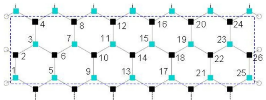
condition. Charge transport is assumed to occur only inside the GNR, which can be considered to be a periodic structure along the longitudi-nal direction. For an armchair ribbon, the unit cell or slab is made of two rows of dimers. Its length is equal to 3 aCC where aCC = 1.42 ˚Ais the
carbon interatomic distance. For reference, a slab taken from an NA = 13
armchair GNR, with NA is the number of dimers in the slab, is illustrated
in fig.1.1. The TB Hamiltonian is introduced to quantum-mechanically describe the electron dynamics inside the GNR. A a set of orthogonal pz
orbitals, one for each carbon atom, is in general sufficient to describe trans-port in graphene-related materials. Indicating with |l, αi the orbital asso-ciated with the atom α within the slab l, the generic matrix element of the Hamiltonian Hlα,mβ is written as
hl, α|H|m, βi = tlα,mβ+ δlα,mβ Ulα (1.1)
where δlα,mβ is the Kronecker delta and Ulα is the electrostatic potential
energy at the (l; α) atom site. The parameter tlα,mβi is usually taken as a
fitting parameter with respect to DFT: for graphene, one can obtain an ac-curate model by setting the t|lα,mβi = t1 if the atoms (l; α) and (m; β) are
first nearest neighbors, and equal to zero otherwise. In this work the approach proposed by [17] has been followed: t1 has been taken equal to -2.7 eV for the internal atom pairs and modified with a factor δ equal to 0.12 eV for the atom pairs along the edges of the GNR, to describe the pas-sivation of the edges by hydrogen atoms. In the real space (RS) approach, the transport problem is formulated within the NEGF formalism [18, 19] using the Hamiltonian described above. The retarded Green’s function Gr
at the energy E is defined by
[(E + iη)I − H]Gr = I (1.2)
with η an infinitesimal positive quantity. For convenience, the quantity A will be defined, with A = (E + iη)I − H. The matrix equation 1.2 is of infinite dimension because it describes the entire structure made of the device region plus the two semi-infinite source and drain leads. It can be proved [18] that if one can solve the problem in the leads, namely
AS gSr = IS (1.3)
AD grD = ID (1.4)
then it is possible to define two self-energies ΣrSand ΣrD:
ΣrS = ACS gSr ASC (1.5)
ΣrD = ACD gDr ADC (1.6)
where ACS defines the matrix that couples the source and the channel.
Similar expressions hold for ASC, ACD, ADC. The problem in the device
region therefore becomes
(AC− ΣrS− ΣrD) GrC = IC (1.7)
Indicating GrC with Grand explicitating the dependence on energy, eq.1.8 takes the form:
[(E + iη)I − HC− ΣrS(E) − ΣrD(E)]Gr(E) = I (1.8)
Assuming that the electrostatic potential in the first and last slabs of the device region is replicated periodically in each slab of the semi-infinite source/drain lead, the self-energies Σr
S and ΣrD can be numerically
com-puted using the iterative algorithm proposed in [20]. In the simulations presented in this thesis, the convergence factor has been set equal to zero inside the device region (in order to guarantee current conservation) and
to 10−7 eV in the leads.
The electron/hole correlation functions are given by
G</>(E) = Gr(E)[Σ</>S (E) + Σ</>D (E)]Ga(E) (1.9) where Ga= Gr†is the advanced Green’s function († represents the
Hermitian-transpose operator).
The self-energies Σ</>S (E) describe the in-scattering of electrons/holes from the source lead into the device region and, according to the previously mentioned hypothesis of thermalized contacts, are given by
Σ<S(E) = i ΓS(E) fS(E) (1.10)
Σ>S(E) = −i ΓS(E) [1 − fS(E)] (1.11)
where ΓS = Σr− Σais the broadening function and
fS(E) =
1 exp(E−EF S
kBT + 1)
(1.12) is the the Fermi function of the source lead and kB is the Boltzmann
con-stant. Analogous expressions can be used for the drain lead, with appro-priate substitutions. A common temperature T is assumed for both con-tacts. From eq.1.9, one can calculate the electron and hole numbers at the (l; α) atom site as nlα = −2i Z ∞ Ei(l,α) 1 2π G <(l, α; l, α; E) dE (1.13) plα= 2i Z Ei(l,α) −∞ 1 2π G >(l, α; l, α; E) dE (1.14) where Ei(l; α) is the intrinsic Fermi level, assumed equal to the potential
energy U∗
lα, and the factor of 2 is due to spin degeneracy. Finally, the
cur-rent is calculated as IDS = 2q h Z ∞ −∞ 2ℜ{T r[H(l, l + 1)G<(l + 1; l; E)]} dE (1.15) where h is the Planck constant and symbols ℜ and T r indicate the real part and the trace on the orbital index, respectively. Since only coherent transport is considered here, it can be proved that eq.1.15 is also equivalent to IDS = 2q h Z ∞ −∞
where T(E) is the transmission function of the Landauer formalism [18] T(E) = T r[ΓSGrΓDGa] (1.17)
It is worth observing that, since H is a block-tridiagonal matrix, with each block representing the coupling between two adjacent slabs, the only non-null block of Σr
S is the first term ΣrS(1, 1), while the only non-null block of
Σr
D is the last term ΣrD(N, N ), with N the number of slabs in the simulation
domain. As a consequence, by directly expanding 1.13, 1.14 and 1.16, it can be obtained that the only blocks of Gr which are needed to compute
charge and current are those related to the first and last columns, i.e. Gr i,1
and Gri,N with i = 1. . .N. Therefore, a recursive algorithm can be used to
compute only those blocks [19].
From the computational point of view the real-space tight-binding is heavy, since it involves the calculation of the elements and the inversion of square matrices whose size is equal to the number of orbitals in each slab. Since the model proposed here is based on a single pzorbital approximation, the
dimension of the matrices turns out to be equal to the number of atoms in each slab. For example, for a GNR with smooth edges with NA=13, the
di-mension of the generic matrix is 26. It is apparent that this approach is not suitable for the simulation of wide GNRs. Since the purpose of the work is to perform a simulation study on GNR-FETs with width up to 15 nm (cor-responding to NA= 124), this poses the need of finding an approximate
but accurate model to limit the use of real space method. As similar meth-ods in literature, mode-space tight-binding is characterized by a change of representation from real space (RS), where the unknown quantities and the Hamiltonian are expressed in terms of atomic orbitals, to mode-space (MS), where the basis is composed of a convenient subset of the transverse eigenvectors (modes).
Given a unitary matrix V, 1.8 in the real space can be transformed into an MS equation of the type:
[(E + i0+)I − fHC− fΣrS(E) − fΣrD(E)]fGr(E) = I (1.18)
where the quantities indicated byeidentify the representations in the mode-space of the corresponding quantities in the real mode-space. For example,
f
HC = V†HCV (1.19)
f
Gr(E) = V†Gr(E)V (1.20)
Similar expressions hold for fΣr
S(E) and fΣrD(E).
Once fGr(E) is known, the RS solution can be easily reconstructed by
1.18 instead of 1.8 is computationally advantageous if fHC can be written
as a block diagonal matrix apart from an index reordering, thus giving rise to an independent problem for each block (mode decoupling). An ad-ditional simplification is achieved if only a subset of these independent problems gives a significant contribution to Gr in the simulated energy window, thus allowing one to neglect the other blocks (mode truncation). Clearly, the efficiency of the MS method depends on the degree with which these two simplifications can be accurately performed. Thus, the selection of the modes to be retained in the calculations and the identification of the coupled and uncoupled modes play a crucial role in the MS approach. Here the transformation matrix V has been chosen as a block diagonal matrix, which has in the columns of its block of index l the orthonormal eigenvectors at k = 0 (modes) of the slab l, computed with the electro-static potential made periodic along the longitudinal direction. Regard-ing the mode couplRegard-ing of an ideal armchair GNR with uniform electro-static potential (the Hamiltonian of which is periodic), it can be studied by comparing the band structure of the RS Hamiltonian with that of the MS Hamiltonian obtained with a specific mode selection, i.e. using a spe-cific subset of the eigenvectors at k = 0 (group of modes) as columns of the generic diagonal block of the transformation matrix. If the selected modes are sufficient to accurately reproduce the desired portion of the RS band structure, it means that it is reasonable to consider them uncoupled from the others. In this work, the approach proposed by [21] has been followed: first the modes are split into several groups and a mode is considered to be coupled only with the other modes within the same group but not with the ones belonging to different groups (decoupling criterion). Secondly, only the groups containing at least one of the Nblowest energy conduction
modes or one of the Nbhighest energy valence modes are retained
(trunca-tion criterion), where Nb is the number of conduction/valence band pairs
that are required to be computed with sufficient accuracy. The algorithm is then used for the selection of modes prior to the simulation of devices with regular GNRs, namely GNRs made of the periodic repetition of an elemen-tary slab. Since the presence of a non-uniform potential along the axis of a regular GNR does not represent a serious cause of mode coupling, selec-tion criteria based essentially on the observaselec-tion of the eigenvalues with constant potential are in general sufficient [22]. Remarkably, although the formulation of the model has been presented energy per energy, the pro-posed method is applicable to the case of incoherent scattering as well.
1.2
Inclusion of electron-phonon interaction
The electron-phonon interaction is included within a perturbative model within the self-consistent Born approximation. Thus, the phonon system is considered unperturbed by the interactions with the electron gas, there-fore the self-energy induced by the presence of phonon scattering can be expressed by:
Σ</>ph = G</>D</> (1.21)
with D</> the less-than and greater-than Green’s functions of the unper-turbed phonon bath. In eq. 1.21, real space is assumed and the explicit dependence on energy is omitted. Details on the explicit calculation of Σ</>ph can be found in [18]. Remarkably, the solution of the kinetic equa-tions requires also the knowledge of the retarded self-energy Σr, that can
be calculated from the relation [23]: Σr(E) = P Z 1 2π Γ(ǫ) E− ǫ − i Γ(E) 2 dǫ (1.22)
where P is a principal value integral on the complex plane, and Γ is defined as
Γ(E) = i[Σ>(E) − Σ<(E)] (1.23) The real part of Σr, represented by the first term of the right side of 1.22, is a non-hermitian energy contribution giving a shift of the particle energy levels, while the second term is associated to the the scattering rate due to the electron-phonon interaction. Therefore, the evaluation of 1.22 can be performed analytically only for the case of elastic scattering while requir-ing a numerical evaluation of the principal value integral in the case of inelastic scattering process. Since this calculation can be computationally expensive due the necessity of the simultaneous knowledge of the Green’s functions for any energy, its contribution is generally omitted. The impact of this assumption has been investigated in [24]. Thus, generally eq.1.22 is well approximated with
Σr(E) ≈ −iΓ(E)
2 (1.24)
It is important to notice that the relations above introduce a dependence of Σron G<. This implies, that in presence of the electron-phonon interaction
eq. 1.8 and
G</> = GrΣ</>Gr† (1.25)
are coupled through a non linear relation. While in the ballistic case those two equations separately describe the dynamics and the statistical proper-ties of the system, when the phonon scattering is included, a self-consistent iterative solution of the two equations with the phonon self-energy func-tions is required.
1.2.1
Acoustic phonon scattering
As far as the scattering with acoustic phonons is concerned, the term Σr ph=
Σr
AP reads, in the real space approach [18]:
ΣrAP(iα, jβ) = KAP Gr(iα, jβ)δijδαβ (1.26) where KAP is given by KAP = DAPkBT mcvs2 (1.27) in which DAP is the deformation potential, kB is the Boltzmann constant,
T is the absolute temperature, mc is the carbon atom mass and vs is the
sound velocity in carbon. The phonon parameters for the 2D graphene longitudinal acoustic mode are employed [25], namely DAP = 16 eV and
vs approximated to 2 · 104 m s−1. According to the change of basis set in
the mode space gΣr
AP can be obtained as:
ΣrAP′ = V†ΣrAPV (1.28) Therefore, g Σr′ AP(iα, jβ) = X lγ,mδ [Viα,lγ† Σr AP(lγ, mδ)Vmδ,jβ] (1.29) thus ΣrAP′ (iα, jβ) = KAP X l,γ [Viα,lγ† Gr(lγ, lγ)Vlγ,jβ] (1.30)
Since V is a blockdiagonal matrix, it holds:
Viα,lγ = δi,lVi(α, γ) (1.31)
where δi,lis the Kronecker delta. Then the RHS of eq.1.30can be written as
KAP
X
γ
[Vi†(α, γ)Gr(iγ, iγ)Vi(γ, β)δi,j] (1.32)
Thus, for each slab it results: g Σr AP(α, β) = KAP X γ [V†(α, γ)Gr(γ, γ)V γ, β] (1.33) Since Gr= V fGrV† (1.34) it results: Gr(γ, γ) =X λ,µ [V (γ, λ)fGr(λ, µ)V†(µ, λ)] (1.35)
By replacing Gr(γ, γ) from 1.35 in eq.1.33, it results: g Σr AP(α, β) = KAP X γ,λ,µ [V†(α, γ)V (γ, λ)fGr(λ, µ)V†(µ, γ)V (γ, β)] (1.36)
Thus, by considering only diagonal terms of fGr, eq. 1.36 is approximated
to: g Σr AP(α, β) ≈ KAP X λ f Gr(λ, λ)X γ [V†(α, γ)V (γ, λ)V†(λ, γ)V (γ, β)] (1.37)
Finally, within the approximation of gΣr
AP as a blockdiagonal matrix, eq.1.37
is approximated with: g Σr AP(α, α) ≈ KAP X λ f Gr(λ, λ)X γ [V†(α, γ)V (γ, λ)V†(λ, γ)V (γ, α)] (1.38) Therefore g Σr AP(α, α) ≈ KAP X λ [fGr(λ, λ)I(α, λ)] (1.39)
where the form factor I(α, λ) is defined as I(α, λ) =X
γ
[V†(α, γ)V (γ, λ)V†(λ, γ)V (γ, α)] (1.40) that, exploiting the following property of the matrix V,
V†(i, j) = V⋆(j, i) (1.41)
can be written as
I(α, λ) =X
γ
[V∗(γ, α)V (γ, λ)V∗(γ, λ)V (γ, α)] (1.42) in which the terms are scalar. Therefore the commutative property can be applied, thus obtaining
I(α, λ) =X
γ
[|V (γ, α)|2|V (γ, λ)|2] (1.43) For reader’s ease, the explicit dependence of energy has been omitted. As pointed out in [26], care must be taken in dealing with the lead self-energies Σr
S/D when phonon scattering is active, in order to avoid
unphys-ical discontinuities near the injecting boundaries. For the determination of ΣrS/D, instead of adopting an iterative procedure based on an analytical approximation of Gr in the leads as in [26], in this work a fully numerical
Figure 1.2:Density-of-states vs.energy computed in the presence of elastic phonon scattering in a uniform NA = 12 intrinsic GNR in three
dif-ferent locations: inside the source lead, inside the drain lead, and in the middle of the device.
iteration procedure has been used. In essence, after a preliminary calcula-tion of Σr
S/D based on an approximation of Gr pertinent to homogeneous
and infinitely long leads, the loop is entered for the self-consistent cal-culation of Gr in the inner domain. At each iteration step, the phonon self-energy blocks relative to the slabs adjacent to the leads are used to recalculate ΣrS/D. Then the procedure is iterated until global convergence is achieved. Fig.1.2 illustrates the LDOS vs. energy calculated in a uni-form GNR at zero bias at three different longitudinal coordinates, namely within the source lead, within the drain lead, and inside the solution do-main. The three overlapping curves demonstrate the consistency of the global solution. From the inset one can appreciate the effect of energy smoothing due to phonon scattering, with the suppression of the singu-larities at the subband edges.
As far as computational cost is concerned, in the mode-space represen-tation the relation between phonon self-energies and Greens functions is more complex than in real space, since scattering tends to couple modes. Therefore, the possibility of a simplifying assumption to reduce the com-putational complexity has been tested. It consists in replacing the phonon self-energies with their respective slab-by-slab averages prior to MS con-version, thus approximating I(α, λ) in eq. 1.43 with 1/NA. As an example,
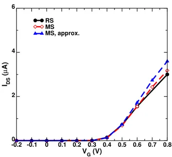
in fig. 1.3 the turn-on characteristics of a GNR-FET with gate length equal to 17 nm and NA= 13 are illustrated. Approximating the I(α, λ) in eq. 1.43
-0.2 -0.1 0 0.1 0.2 0.3 0.4 0.5 0.6 0.7 0.8 VG (V) 0 2 4 6 IDS ( µ A) RS MS MS, approx.
Figure 1.3:Turn-on characteristics of a GNR-FET with gate length equal to 17 nm and NA= 13 at VDS = 0.1 V, simulated accounting for AP scattering.
Simulations were performed with the real space (closed circles, solid black line), mode-space with form factor fully computed (MS: open di-amonds, dashed red line) or approximated to be constant (MSapprox;
closed triangles, dashed blue line) approaches.
if I(α, λ) is correctly computed, the discrepancy between the mode-space and real-space approach is almost negligible. Therefore in this work, oth-erwise stated, the complete formulation of I(α, λ) will be used as far as the scattering with acoustic phonons is concerned.
1.2.2
Optical phonon scattering
Regarding the inclusion of optical phonon scattering, it is worth highlight-ing that the energy levels that differ for the energy of the optical phonon become all coupled. Therefore the calculations described above become definitely more involved, as energies can not be considered as separate, but the simulation must take into account sets af energies instead of sin-gle energy levels. Apart from the computational burden, the treatment of optical phonons is quite straightforward and an expression similar to 1.26 can be considered: ΣrOP(iα, jβ) = KOP Gr(iα, jβ)δijδαβ (1.44) where KOP is given by KOP = (Dtk¯h)2 (2mc∆E) (1.45)
with Dtk is the deformation potential, ¯h the reduced Planck constant, mc
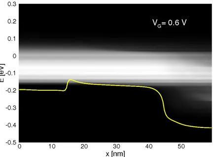
the carbon atom mass and ∆E the energy of the phonon. In this work, only optical phonons corresponding to a phonon energy ∆E equal to 160 meV [27] have been included. Fig. 1.4 depicts the turn-on and output charac-teristics of an armchair GNR-FET with double-gate geometry and with 2.5 nm-thick HfO2layers. NA=16 and the gate length is equal to 30 nm. Source
and drain regions are 30 nm long, with a doping density of 0.5 dopant per nm. Since in [33], devices with the same features were investigated by means of a real space approach, results in [33] can be taken as a benchmark to verify the accuracy of our model. From the current-voltage character-istics shown in fig. 1.4, one can assert that our simulations, performed in the mode-space approach, very well reproduce the results obtained for the full real-space even at high gate/drain voltage. The difference between the models is slightly larger at high drain voltage, where the coupling between modes becomes more involved. The phonon contribution at different bias can be understood by plotting the current flow. In figs.1.5 and 1.6 the cur-rent densities vs. longitudinal coordinate for the device presented above, at VDS= 0.3 V for different gate voltages, namely VG= 0.4 V and VG= 0.6 V,
are illustrated. As observed in [33], while at low gate voltage the contribu-tion of optical phonons is negligible, it becomes more important at higher VG, since a significant number of injected carriers have empty states
avail-able for scattering. Therefore an optical phonon can be emitted. Since as gate voltage increases, the number of available states increases, scattering with optical phonons is expected to affect performance more at higher gate voltages, as shown in fig. 1.4, lower panel.
0 0.1 0.2 0.3 0.4 0.5 0.6 0.7 0.8 VG (V) 0 2e-06 4e-06 6e-06 8e-06 1e-05 1.2e-05 1.4e-05 1.6e-05 1.8e-05 2e-05 ID (A) MS, 2 gr acc Yoon, APL VD = 0.3 V 0 0.1 0.2 0.3 0.4 0.5 VD (V) 2e-06 4e-06 6e-06 8e-06 1e-05 1.2e-05 1.4e-05 ID (A) MS, 2 gr acc Yoon, APL VG = 0.6 V
Figure 1.4:Turn-on characteristics at VDS = 0.3 V and output characteristics at
VDS = 0.6 V of a GNR-FET with NA= 16. The geometry of the
sim-ulated device is the same as proposed in [33], accounting for AP and OP scattering. Both our simulation results (blue line, closed symbols) and results in [33] (red line, open symbols) are reported.
Figure 1.5:Computed current density at VG= 0.4 V, VDS= 0.3 V for a GNR-FET
with NA= 16 with the same parameters as listed in [33], with the
acti-vation of acoustic and optical phonon scattering.
Figure 1.6:Computed current density at VG= 0.6 V, VDS= 0.3 V for the same
1.3
Self-consistency of potential solution
Finally, the electrostatic potential energy Ulαentering into the Hamiltonian
is calculated by self-consistently solving the 3D Poisson equation. The box integration method is used on a discretization grid of prismatic elements with a triangular base, matching the hexagonal graphene lattice. The elec-tron and hole charge given by 1.13 and 1.14 is directly assigned to the box surrounding the (l; α) atom. Otherwise stated, the self-consistency of the potential solution has been achieved with a precision of 0.01%.
1.4
Summary
In this chapter, the formulation of the tight-binding NEGF method has been presented, along with considerations above the inclusion of the electron-phonon interaction. Given the high computational cost of the model, rea-sonable approximations to improve speed-up have been discussed.
Chapter 2
GNR-FETs for digital applications
In recent years, graphene nanoribbons (GNRs) have been the object of large investigation for nanoelectronic applications, as they potentially com-bine the attractive features of graphene with the possibility of energy gap engineering [16] due to quantum confinement. Besides, since the energy band-gap, as previously discussed, scales inversely with the width of the GNR, only very narrow GNRs (1 to 3 nm-wide) have been proposed to be suitable for digital applications that require high ION/IOF F ratio. On
the other hand, the inevitable edge roughness (ER), related with the tech-nological issue of controlling the edges with atomic precision, seriously reduces the performance of GNR-FETs [29]. Given the difficulty of exper-imental verification, numerical simulation can greatly help to understand the essential features of transport in GNR devices in the presence of ER as well as of other defects and scattering centers. Recently, the GNR mobility has been studied by means of semi-classical approaches [30, 31, 32] and full GNR-FETs simulations accounting for ER have been carried out using quantum transport atomistic methods [33, 34], showing a dramatic current reduction in the ON-state. In [35], the GNR-FET mobility has been inves-tigated combining direct atomistic simulations of GNR-FETs affected by ER, as well as other types of point defects, by using semianalytical expres-sions for the phonon-limited mobility, showing that phonons and ER are the main causes of mobility reduction in very narrow GNR-FETs. In this chapter, the full-quantum transport model described in chapter 1 has been used to perform a simulation study on the transport properties of 1 to 2.5 nm-wide GNR-FETs. For GNR-FETs with perfectly smooth edges, the sim-ulations have been performed in the mode-space approach (see chapter 1), which is a very good trade-off between numerical accuracy and simulation speed-up, while for GNR-FETs affected by edge roughness, the real space formulation has been adopted, to fully account for mode coupling [21]. In section 1, the device under investigation will be presented; the results of the simulations with the inclusion of elastic phonons will be discussed in
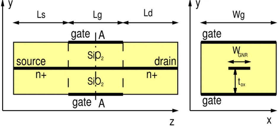
SiO2
source
drain
n+
n+
y
gate A
A
gate
z
y
gate
gate
x
tox Ls Lg Ld Wg W SiO GNR 2Figure 2.1:Longitudinal and transverse cross-sections of the simulated
GNR-FETs.
sec. 2, while in sec. 3 the performance of GNR-FETs with rough edges will be investigated.
2.1
Simulated structure
The simulated structure is presented in fig.2.1: the device presents a double-gate topology with very thin oxide layers (silicon oxide thickness tox has
been set to 1 nm), in order to maximise the electrostatic control over the channel. The symmetric 10 nm-long source and drain regions have been simulated by considering semi-infinite doped leads, while the channel has been assumed intrinsic. The doping concentration for source and drain regions has been fixed at 10−2 dopant atoms/carbon atoms. The
nomi-nal number of atomic dimers in the slab NA, that defines the GNR width
(WGN R), and the gate length LGhave been taken as variable parameters in
the study.
2.2
Effect of acoustic phonons
The inclusion of acoustic phonons (AP) in the transport model results in the suppression of the singularities of the density of states at the edge of the subband, as shown in fig.1.2. This induces a smoothing effect on the profile of the density of states, as apparent in fig. 2.2, that depicts the com-puted local density of states of a GNR-FET with NA= 13 and LG= 17 nm
at a given bias with and without the inclusion of acoustic phonons. The energy-smoothing effect due to phonons is clearly visible, especially in the quasi-bound states of the valence band within the channel.
Figure 2.2:Local density of states within a GNR-FET in the ballistic regime (up-per panel) and with elastic phonon scattering (lower panel) for a GNR-FET with NA= 13 at VG= 0 V, VDS= 0.5 V.
the ribbon, and from the interfaces with the underneath and top gate in-sulator layers are ignored. The latter assumption is justified in case of sus-pended GNRs. Fig. 2.3 illustrates the turnon and output characteristics of a GNR-FET with NA= 13 and LG= 20 nm, computed with and without the
inclusion of phonon scattering, in the case of ideal edges. From the com-parison with the ballistic case, it is observed that the effect of AP scattering is not negligible, in spite of the small gate length. From fig. 2.3, the ballis-ticity ratio, calculated at VG= 0.8 V, results as small as about 0.6. The reason
for this can be attributed to the small width of the GNR (W= 1.5 nm), and to the phonon scattering rate, that is expected to be inversely proportional to the GNR width [30]. For completeness of the study, fig. 2.4 depicts the turnon characteristics at VDS= 0.5 V and 1 V. Although AP scattering
-0.2 -0.1 0 0.1 0.2 0.3 0.4 0.5 0.6 0.7 0.8 VG (V) 0 2 4 6 IDS ( µ A) Bal AP 0 0.2 0.4 0.6 0.8 VDS (V) 0 2 4 IDS ( µ A) bal AP
Figure 2.3:Turnon characteristics at VDS= 0.1 V (left panel) and output
character-istics at VG= 0.6 V (right panel)for a GNR-FET with NA= 13 and LG=
20 nm simulated under ballistic conditions (solid lines) and account-ing for AP scatteraccount-ing (dashed lines).
VDS= 0.5 V shown in fig. 2.4 and the good current saturation performance
with respect to VDS, shown in the right panel of fig. 2.3, confirm the great
potential of narrow GNR-FETs for digital applications. At very high drain voltages, remarkable accumulation of holes in the channel due to band-to-band tunneling occurs. As a consequence of this phenomenon, it is not possible to turn the device off, as evident in fig. 2.4 for VDS= 1 V. For wider
nanoribbons the performance limitations due to holes pile-up in the
chan--0.2 0 0.2 0.4 0.6 0.8 VG (V) 10-14 10-12 10-10 10-8 10-6 10-4 IDS (A) VDS = 1 V VDS = 0.5 V
Figure 2.4:Turnon characteristics at VDS= 0.5 V (red triangles) and VDS= 1 V
(blue diamonds) in ballistic conditions (solid lines) and accounting for AP scattering (dashed lines). The device parameters are the same used in fig. 2.3.
0 50 100 150 LG (nm) 0 500 1000 1500 2000 2500 Mobility (cm 2 /Vs) Bal AP AP, extr.
Figure 2.5:Effective (red open symbols, solid line), ballistic (black closed sym-bols, solid line) and AP-limited (red open symsym-bols, dotted line) mo-bilities at low-field as a function of the gate length for a GNR-FET with NA= 13 and VGS = 0.6 V.
nel become more severe, as will be discussed in the next chapter.
The effective low-field mobility can be extracted from the current-voltage characteristics of devices with different gate lengths, as illustrated in fig. 2.5 for a GNR-FET with NA= 13. The drain voltage has been set to 10 mV.
This results in the device operating in linear regime. In this work mobility has been calculated as a function of gate length from the expression
IDS =
µQchVDS
LG
(2.1) where Qch is the average electron charge in the channel per unit length.
A strong mobility reduction induced by phonon scattering is apparent. In addition, from the mobilities calculated under ballistic conditions and with AP scattering, the AP-limited mobility is extracted vs. gate length assuming the validity of Matthiessen’s rule (dotted line in fig. 2.5). The extracted long-channel values are collected in fig.2.6 as a function of NA
for VG= 0.6 V, corresponding to the device operating in ON condition. The
extracted mobility values turn out to be almost proportional to NA and
divided in two sets according to the different family of seminconducting GNRs, namely the ones with NA= 3n and 3n+1, respectively. As expected,
mobility increases with device width in both families.
As far as the mobility dependence on VGis concerned, the increase of gate
voltage results in a mobility reduction, as illustrated in fig. 2.7. This can be explained on the basis of the Landauer conductance expression, which
12 14 16 18 20 22 NA 0 500 1000 1500 2000 2500 Mobility AP (cm 2 /Vs) 3n 3n+1
Figure 2.6:Extracted effective AP-limited mobility as a function of NA at VG=
0.6 V. The orange and green lines connect the points belonging to the family of NA= 3n and 3n+1, respectively.
holds for elastic scattering processes. In fact, when the channel is driven more and more into degenerate conditions, the carrier concentration in the channel increases with VG faster than the conductance, which ultimately
tends to saturate at high gate bias. Hence, mobility decreases.
0.4 0.5 0.6 0.7 VG (V) 0 500 1000 1500 2000 2500 3000 3500 Mobility (cm 2 /Vs) 0.4 0.5 0.6 0.7 VG (V) 0 500 1000 1500 2000 2500 3000 3500 Mobility AP (cm 2 /Vs) NA = 12 NA = 13 NA = 15 NA = 16 NA = 21 BAL AP
Figure 2.7:Mobility in ballistic conditions and with AP scattering (left panel) and extracted effective AP-limited mobility (right panel) as a function of VGfor GNR-FETs with different NA.
2.3
Effect of edge roughness
As proposed in [36], edge roughness is treated in the model by adding or removing dimers independently along each edge of the GNR according to a predefined probability P, that in this study is set equal to 5%. To take partially into account the statistical variance of the results, each simulation has been repeated five times, each time with a different ER implementa-tion. Due to the computational cost, that is quite high even for very narrow GNR-FETs, the self-consistent solution with Poisson equation has not been sought. Instead, the electrostatic potential has been determined from the self-consistent ballistic simulation of the nominal GNR-FET with perfectly smooth edges. Fig. 2.8 collects simulation results for devices with rough edges, with nominal NA= 13 and 21, with and without the inclusion of
elastic phonon scattering. The reference bias is VG= 0.6 V, VDS= 10 mV.
Interestingly, for the narrower device, when ER only is active, the current decreases almost exponentially with respect to LG, much faster than the
∝ 1/LG ohmic law, which suggests the presence of a strong localization
regime due to quantum interference. When AP scattering is included in the picture, the effect is to break quantum coherence, therefore the current increases. Moreover, the variance is significantly reduced. Thus, a nearly,
20 40 60 80 100 120 140 LG (nm) 1e-12 1e-11 1e-10 1e-09 1e-08 1e-07 1e-06 1e-05 IDS (A) ER ER+AP
ballistic, smooth edges
1/LG extrapolation
NA = 13
NA = 21
Figure 2.8:Current vs. gate length of NA= 13 (blue diamonds) and NA= 21 (red
circles) GNR-FETs at VG= 0.6 V, VDS = 10 mV, simulated with edge
roughness (ER) with P = 0.05 (solid black lines, closed squares), with ER + AP scattering (solid red curve, closed circles), and in the ballistic regime with smooth edges (dotted lines). The green dashed curves are 1/LGextrapolations through the LG= 110 nm ER+AP curves. The
but not fully, diffusive regime is recovered, as indicated by the comparison with the dashed curve, which is a 1/LGextrapolation. Similar results have
been found e.g. in [37], focused on the investigation of silicon nanowires with very small cross-sections. For the GNR with NA= 21, the impact of
the edge roughness is still not negligible, but the dependence on the gate length is weaker. Also, ER has much less impact with respect to the nar-rower case, as indicated by the quite small variance as well as by the fact that the current levels in ER + AP condition are lower than in the ER case. This is expected in a diffusive transport regime where different scattering mechanisms combine to limit current. The results for the NA= 13 and NA
= 21 GNR-FETs at VG = 0.6 V are µ ≈ 17 cm2/Vs and µ ≈ 307 cm2/Vs,
respectively. When compared with the ones in fig. 2.6, these data confirm the significant impact of ER on mobility. In [29] experimental µ equal to 174 cm2/Vs was reported for a 2.5±1 nm wide-GNR with LG= 110 nm,
which is smaller than the computed data for the NA= 21 device of
compa-rable width and length. A number of reasons can explain the difference, ranging from geometrical uncertainties to the presence of a variety of other scattering centers not included in the model.
For very narrow GNRs, since the current depends almost exponentially on gate length, it is not possible to define an ER-limited mobility and the use of Matthiessen’s rule becomes not suitable. However, the inclusion of elas-tic phonon scattering recovers the diffusive law and reduces the variabil-ity. Therefore, it is possible to extract an equivalent effective ER-limited
0 50 100 150 LG (nm) 0 100 200 300 400 Mobility (cm 2 /Vs) AP ER+AP ER eq., extr. 0 50 100 150 LG (nm) 0 1000 2000 Mobility (cm 2 /Vs) AP ER+AP ER eq., extr.
Figure 2.9:Extracted effective ER-limited mobility (dotted line) vs. gate length for GNR-FETs with different NA=13 (left panel) and NA=21 (right
panel). Low-field mobility data for perfectly smooth (black lines, squares) and rough (red lines, circles) GNR-FETs with AP scattering are reported. The extracted effective ER-limited mobility data have been calculated by subtracting the AP data (that include ballistic com-ponent) from ER+AP data by using the Matthiessen’s rule.
mobility by using the Matthiessen’s rule over the mobility data in case of smooth and rough GNR-FETs with the inclusion of AP. In fig. 2.9 the ex-tracted effective ER-limited mobility for GNR-FETs with NA= 13 and NA=
21 are reported. It is apparent that edge roughness affects performance definitely more than elastic phonon scattering. Finally, the study has been extended to GNR-FETs with different NA. Because of the high
compu-tational cost of the simulations, the approach adopted in this section has been to perform simulations at selected energies, without striving for self-consistency of the solution. In particular, transmission coefficients at two energy levels have been computed. The chosen energy levels have been E= 0.1 eV (with respect to the energy reference, that is the Fermi level in the source), and the energy that corresponds to the kinetic energy equal to 0.1 eV with respect to the bottom of the conduction band in the channel. Therefore, while the first energy level is fixed for different NA, the second
changes, according to the different electrostatics of the system. The ad-vantage of this simulation approach has been to provide a significant im-provement of the statistic, moving from 5 to 50 repetitions per data point. The obtained results are illustrated in fig. 2.10. Since the variance of hln T i is small, the errors bars are not reported in the picture. That also confirms that strong localization regime occurs in very narrow rough GNR-FETs even at short lengths, as it holds:
∆ln T
hln T i ≪ 1 and ∆ T
hT i ≫ 1 (2.2)
However, as shown in the left panel of fig. 2.10, the partial recovery of diffusive law gradually occurs as width increases, for GNRs belonging to the same family. In fact, devices with NA= 12 show strong
localiza-tion, that progressively decreases as width increases to NA= 15 and then
NA= 21. The dependence of the average logarithm of transmission on NA
for GNRs belonging to different seminconducting families, namely NA=
3n and 3n+1, is more involved. In fact, the curve related to GNR-FETs with NA= 12 report current levels higher than for the ones for NA= 13.
Data computed for kinetic energy= 0.1 eV are in line with these consider-ations, thus suggesting a very involved relation between transmission at any given energy and NA. That results in a quite intricate dependence of
the current on GNR width, as far as GNRs with rough edges are consid-ered.
To complete the study, the localization length ξ has been calculated for the GNR-FET with NA=13, for which the strongest localization regime at any
given computed energy has been observed. In this regime, a well-defined statistical quantity is provided by hln T i with
hln T i ≈ −L
where ξ is the localized length [38]. In equation 2.3, L is the length of the disordered region; hence, in this study it is equal to the gate length. The localization length has therefore been extracted through numerical fitting for five different energies, corresponding to kinetic energy varying from 0.1 eV to 0.5 eV. The plots of the transmission coefficient with respect to gate length and the fitting curves are presented in fig. 2.11, while the fitting values are collected in table 2.1. One can observe that longer lo-calization lengths correspond to higher energy levels, as the number of active channels increase. In table 2.2 the fitted values for ξ for different energies and NA are summarized. While for GNR-FETs with NA= 13 the
ξis quite low for both the computed energies, it significantly increases for NA= 12. Confirming the considerations presented above regarding current
performance for NA= 13 and NA= 21 devices, for both families ξ at a given
energy increases as GNR width increases. In [38], focused on a simula-tion study on armchair GNRs with NA= 27 and roughness probability set
to 7.5% for different types of disorder, extracted localization lengths were in the range between 10 and 40 nm, according to the disorder profile, thus suggesting a very small robustness of armchair GNRs to ER. In [38], the large variability of the extracted data was also due to the fact that in the energy region where only one channel is active, the strongest deviations were observed. Moreover, as the roughness probability inversely impacts the performance, extracted mean free paths (and localization lengths) var-ied of more than one order of magnitude when the roughness probability
0 50 100 150 LG (nm) -25 -20 -15 -10 -5 0 < ln T > N A = 12 NA = 13 NA = 15 NA = 16 NA = 21 0 50 100 150 LG (nm) -25 -20 -15 -10 -5 0 < ln T > N A = 12 NA = 13 NA = 15 NA = 16 NA = 21
Figure 2.10:Averaged logarithm of the transmission coefficient vs. gate length for GNR-FETs with different NAranging from 12 to 21 at energy= 0.1 eV
(left panel) and kinetic energy= 0.1 eV (right panel) at the reference bias point VG= 0.6 V, VDS= 10 mV. Solid lines with closed symbols
mark ER data, while dotted lines with open symbols indicate ER+AP data. As the statistic is quite accurate, the error bars are not reported in the picture.
0 50 100 150 LG (nm) -25 -20 -15 -10 -5 0 < ln T > E Kin = 0.1 eV EKin = 0.2 eV EKin = 0.3 eV EKin = 0.4 eV EKin = 0.5 eV
Figure 2.11:Transmission coefficient vs. gate length of NA= 13 GNR-FETs at VG
= 0.6 V, VDS = 10 mV for selected energies corresponding to kinetic
energies ranging from 0.1 eV to 0.5 eV (solid curves, closed sym-bols). The fitting curves are shown in the same colour, by using dot-ted lines. Ekin[eV ] ξ[nm] 0.1 6.9 0.2 11.6 0.3 17.7 0.4 23.4 0.5 25.9
Table 2.1:Fitted values for localization length ξ for GNR-FETs with NA= 13, for
different energies corresponding to kinetic energy (Ekin) ranging from
to 0.1 to 0.5 eV.
NA ξE=0.1eV[nm] ξEkin=0.1eV[nm]
12 24.2 16.4
13 7.2 6.9
15 35.2 26.3
16 15.5 10.9
21 41.2 52.5
Table 2.2:Fitted values for localization length ξ for GNR-FETs with different NA,
was changed from 2.5% to 7.5%.
Considering the large variability of parameters, the localization lengths extracted in this study, which are in the order of several decades of nm, are in line with data available in literature.
2.4
Summary
In this chapter an investigation on current-voltage characteristics and low-field mobility in very narrow GNR-FETs (W ≤ 2.5 nm) has been presented, comparing the effects of edge roughness and acoustic phonons on the performance of those devices. Full-quantum atomistic simulations have been performed, particularly oriented to the investigation of the low-field transport regime. Although the effect of elastic phonon scattering on cur-rent is not negligible even at small gate lenghts, very narrow GNR-FETs show good potential to be used in digital applications, due to their high ION/IOF F ratio and good current saturating behaviour at high drain
volt-age. Regarding the impact of edge roughness, for very narrow GNR-FETs quantum localization effects due to ER are apparent. When AP scatter-ing is activated, a diffusive regime is partially recovered and the statistical variance of the current is also strongly reduced. This represents good news with respect to other studies which, from simulations of GNR-FETs with ER only, had probably overestimated the current variability. However, for such narrow GNR-FETs edge roughness remains the main current limiting effect, degrading mobility much more severely than elastic phonon scat-tering. When phonon scattering is not activated, for very narrow rough GNR-FETs it is not possible to extract ER-limited mobility data. However, equivalent edge roughness-effective mobility values for different NAhave
been provided, by using the Matthiessen’s rule over rough GNRs when acoustic phonon scattering is present and a diffusive regime is recovered. In addition, localization lengths in line with data available in literature have been extracted for GNR-FETs of different widths.
Chapter 3
GNR-FETs for analog applications
It has been shown that a band-gap of several hundreds meV is necessary to achieve the on/off current ratio required in digital applications [39]. This in turn requires graphene nanoribbons (GNRs) with energy band-gaps of several hundreds of meV, shown only in very narrow GNRs (1 to 3 nm-wide) [29, 34, 30]. As discussed in the previous chapter, for such nar-row nanoribbons, mobility performance is strongly limited by the edge roughness and the interaction with phonons [29, 34, 33, 35]. Moreover, successful techniques for the fabrication of those devices are far beyond the state-of-the-art technology, as the latest experiments report GNRs that are from 10 to 30 nm-wide [40, 41, 42, 43, 44]. However, these nanoribbons are less affected than narrower ones by edge roughness, and show higher mobility and better transport properties. These considerations have re-cently pushed the research on graphene and GNRs towards analog high-frequency applications [45, 46, 47, 9, 48, 49, 50, 51], for which achieving high cut-off frequencies is the key point and it is not required to turn the current off. In [52], an extensive study on aspects like stability, gain, power dissipation and load impedance of ballistic graphene GNR-LNAs led to the conclusion that GNRs with the energy band-gap of the order of 100 meV are ideally suited for that application. In this chapter the full-quantum trasport model described in cap. 1 has been used to perform a simulation study on 10 to 15 nm-wide GNR-FETs (which show a 90 to 140 meV band-gap), and to provide design suggestions and optimization criteria. In section 1 the simulated device and its current-voltage charac-teristics will be presented; sec. 2 will be focused on discussing the main causes of the non-saturating behaviour typical of these devices and design criteria will be suggested; in sec. 3 the investigation will be extended to the the simulation of GNR-FETs with metal contacts, and considerations above methods to optimize the performance will be proposed. Finally, in sec. 4 a generalization of the study will be presented, to explore the maxi-mum performance achievable.
SiO2
source
drain
n+
n+
y
gate A
A
gate
z
y
gate
gate
x
tox Ls Lg Ld Wg W SiO GNR 2Figure 3.1:Longitudinal and transverse cross-sections of the simulated
GNR-FETs.
3.1
Performance evaluation
The reference architecture for the device, previously illustrated in 2.1, is reported for convenience in fig.3.1. In this study, 10 nm-wide semicon-ducting GNRs with armchair ideal edges are taken as channel material, and a double-gated structure with silicon oxide 1 nm-thick is investigated. The 10 nm-long source and drain regions are doped with the same doping species while channel is intrinsic, leading to an n-i-n topology. Source and drain doping concentrations are somewhat arbitrary at this stage and will be optimized later. The channel length is short (LG= 10 nm) to seek
high-frequency performance. From the turn-on characteristics depicted in fig. 3.2, it is apparent that the device is not suitable for logic operation, since the largest on/off current ratio is nearly 5. This confirms that 10 nm-wide GNR-FETs are not suitable for logic applications.
The output characteristics presented in fig. 3.3 show the complete absence of a saturating behaviour, i.e. the output conductance
gd =
∂IDS
∂VDS
(3.1) always remains high. The lack of a saturation region results in a strong limitation on the maximum voltage-gain achievable, given by
Av = gm gds , where gm = ∂IDS ∂VGS (3.2) is the transconductance. Besides that, the choice of the bias point becomes critical, since the low gdregion is very narrow. The reason for the absence
of a clear saturation region is illustrated in fig. 3.4 , reporting band di-agrams and current energy spectra relative to the bias points marked A and B in fig. 3.3. Due to the small band-gap (EG= 0.14 eV), at high VDS
0 0.2 0.4 0.6 V G (V) 0 50 100 150 I DS ( µ A) VDS = 0.2 V VDS = 0.4 V VDS = 0.6 V VDS = 0.8 V
Figure 3.2:Turn-on characteristics of a simulated ideal GNR-FET with
source/gate/drain lengths equal to 10 nm each, GNR width equal to 10 nm (corresponding to NA= 82 dimers in the GNR 1D unit
cell), silicon oxide 1 nm-thick, source and drain doping fractional concentrations equal to 5 · 10−3. 0.2 0.4 0.6 0.8 VDS (V) 0 20 40 60 80 100 120 IDS ( µ A) VG = 0.2 V VG = 0.3 V VG = 0.5 V VG = 0.7 V A B
Figure 3.3:Output characteristics of the simulated ideal GNR-FET with the same
parameters as in fig. 3.2. Labels A (at VG= 0.5 V, VDS= 0.4 V) and B
(at VG= 0.5 V, VDS= 0.6 V) indicate the bias points relative to the plots
in fig. 3.4.
the bottom of the conduction band and the top of the valence band are present in the same energy interval. Thus, band-to-band-tunneling (BTBT)
0 10 20 30 40 Long. coord. (nm) -1 -0.8 -0.6 -0.4 -0.2 0 Energy (eV) A, LG = 10 nm B, LG = 10 nm A, LG = 20 nm B, LG = 20 nm 0 100 200 300
Current density (µA/eV)
Figure 3.4:Lowest subband diagram (left) and total current spectral density vs. energy (right) for the device with gate length equal to 10 nm simulated in figs. 3.2 and 3.3 for the two bias points indicated with the labels A and B in fig. 3.3. The curves relative to the simulation of a GNR-FET with gate length equal to 20 nm are also reported. The zero energy reference is the Fermi level in the source.
at the drain-end of the channel takes place such that electrons in the va-lence band in the channel are almost in equilibrium with the Fermi level in the drain. Hence, increasing VDS causes a depletion of electrons in the
va-lence band in the channel, with a consequent positive charge accumulation due to the electrons in the channel escaping to the drain. That, due to the static feedback, induces the reduction of the potential energy barrier which is responsible for the current increase and substantial non-saturating be-haviour. The effect is similar to a Drain-Induced Barrier-Lowering (DIBL) in standard MOSFETs, but in this case the reason is not the occurrence of short-channel effects. In fact, when the gate lenght is doubled from 10 nm to 20 nm, it is observed that the energy barrier height does not depend on LG(fig. 3.4, left panel) and only minor variation occurs in the current
den-sity spectra (fig. 3.4, right panel). Since the lack of saturation is not due to short-channel effects (SCEs), increasing the gate length in GNR-FETs does not improve performance, unlike reported for standard silicon MOSFETs.
![Figure 3: Main orientations of graphene nanoribbons. Image taken from [15].](https://thumb-eu.123doks.com/thumbv2/123dokorg/8192703.127664/12.892.204.661.200.495/figure-main-orientations-graphene-nanoribbons-image-taken.webp)