Universit`
a di Pisa
Scuola di Dottorato in Ingegneria “Leonardo da Vinci”
Corso di Dottorato di Ricerca in
Ingegneria dell’Informazione
Tesi di Dottorato di Ricerca
System-on-chip Computing and
Interconnection Architectures for
Telecommunications and Signal Processing
Nicola Eugenio L’Insalata
Universit`
a di Pisa
Scuola di Dottorato in Ingegneria “Leonardo da Vinci”
Corso di Dottorato di Ricerca in
Ingegneria dell’Informazione
Tesi di Dottorato di Ricerca
System-on-chip Computing and
Interconnection Architectures for
Telecommunications and Signal Processing
Autore:
Nicola Eugenio L’Insalata
Relatori:
Prof. Roberto Saletti
Prof. Luca Fanucci
This file is an extract of the whole work.
Submitted to the Ph.D. Council on February 29, 2008 Accepted for final discussion on March 11, 2008 Final version printed on April 09, 2008
Copyright c 2008 by Nicola Eugenio L’Insalata. All rights reserved.
Permission to make digital or hard copies of all or part of this work for personal or classroom use is granted without fee provided that copies are not made or distributed for profit or commercial advantage and that copies bear this notice and the full citation on the first page. To copy otherwise, to republish, to post on servers or to redistribute to lists, requires prior specific permission.
Ad Anna, Antonio & Enrico A mio nonno, Peppino
I’m ready! (Spongebob Squarepants)
Ringraziamenti
Questa tesi chiude un percorso di tre anni che ha portato in me cambiamenti piccoli e grandi. Sul cammino ho trovato tante persone che mi hanno affiancato ed aiutato a superare gli ostacoli pi`u impegnativi.
Ringrazio innanzitutto i miei tutori, Luca Fanucci e Roberto Saletti per aver reso possibile questo cammino. Un grazie speciale a Luca, per l’attenzione che ha posto alla mia crescita come ricercatore e come persona, guidando e mai limitando le mie scelte.
Grazie a Massimo Rovini, che per primo nel laboratorio di Sistemi Elettronici mi ha guidato ed insegnato.
Grazie a Sergio SAPOnara, per avermi insegnato a distillare idee da quadri mentali ricchi e confusi. Un passo alla volta, una feature alla volta!
Grazie al gruppo NoC a Pisa: Esa Petri, Michele Casula e Francesco Vitullo. Grazie per tutti gli stimoli che mi avete fornito, anche quando non lo sapevate. Grazie per aver testato con estrema pazienza i miei esperimenti (a volte discutibili, devo ammetterlo) di design automation.
Grazie al gruppo Spidergon presso i laboratori AST di STMicrolectronics - Gre-noble: Marcello Coppola, Riccardo Locatelli, Valerio Catalano, Lorenzo Pieralisi, Giuseppe Maruccia e Philippe Teninge. Grazie per avermi dato la possibilit`a di toccare con mano quello che sar`a lo stato dell’arte di domani.
Grazie alle persone che ho a mia volta guidato: Tommaso Cecchini e Gabriele Nobili. Probabilmente vi ho insegnato un decimo di quello che io ho imparato da voi.
Grazie a tutti i miei compagni di viaggio quotidiani durante questi tre anni: Daniele Mangano, Francesco Rossi, Fabrizio Iacopetti, Pierluigi Nuzzo, Federico Baronti, Giuseppe Gentile, Iacopo Del Corona, Tony Bacchillone, Marco Tonarel-li, Luca Mostardini, Luca BacciarelTonarel-li, Francesco D’AscoTonarel-li, Massimiliano Melani, Fernando De Bernardinis, Alessandro Renieri e Ivan Maione. Grazie ad Ivan due volte, perch`e mi ha aiutato quando ero un po’ confuso su dove fosse casa mia.
Grazie a Gianfranco Risaliti, per tutto quello che `e riuscito ad insegnarmi durante un solo mese di lavoro insieme alla Yogitech.
Grazie ai miei amici, ora sparsi un po’ qui e un po’ l`a: Mauro, Giampaolo, Fabio, Laurent, Mimmo (dove sei?), Giulia, Maurizio, Giovanna, Brunello, Stefa-nia, Cristina, Massimiliano F., Andrea, Gabriele, Marco, Simone, Luca, Niccol`o, Nicola, Alex, Barbara, Melissa e Cristiana.
This file is an extract of the whole work.
Grazie ad Alessandra, mio riferimento in questi tre anni. Grazie a Francesca e Giulia, per la loro amicizia. Grazie a chi mi ha sostenuto durante la scrittura di questa tesi.
Grazie alle mie famiglie in Livorno (l’ultima volta che ho scritto questa frase ho usato il singolare).
E per finire, un grazie alla mia famiglia: Anna, Antonio ed Enrico. Grazie per il vostro sostegno, la vostra pazienza, la vostra fiducia in me.
Certo, grazie anche al mio gatto, Igor.
nico
Abstract
This dissertation proposes novel architectures and design techniques targeting SoC building blocks for telecommunications and signal processing applications.
Hardware implementation of Low-Density Parity-Check decoders is approached at both the algorithmic and the architecture level. Low-Density Parity-Check codes are a promising coding scheme for future communication standards due to their outstanding error correction performance.
This work proposes a methodology for analyzing effects of finite precision arith-metic on error correction performance and hardware complexity. The methodol-ogy is throughout employed for co-designing the decoder. First, a low-complexity check node based on the P -output decoding principle is designed and character-ized on a CMOS standard-cells library. Results demonstrate implementation loss below 0.2 dB down to BER of 10−8and a saving in complexity up to 59% with
re-spect to other works in recent literature. High-throughput and low-latency issues are addressed with modified single-phase decoding schedules. A new “memory-aware” schedule is proposed requiring down to 20% of memory with respect to the traditional two-phase flooding decoding. Additionally, throughput is doubled and logic complexity reduced of 12%. These advantages are traded-off with error correction performance, thus making the solution attractive only for long codes, as those adopted in the DVB-S2 standard. The “layered decoding” principle is extended to those codes not specifically conceived for this technique. Proposed architectures exhibit complexity savings in the order of 40% for both area and power consumption figures, while implementation loss is smaller than 0.05 dB.
Most modern communication standards employ Orthogonal Frequency Divi-sion Multiplexing as part of their physical layer. The core of OFDM is the Fast Fourier Transform and its inverse in charge of symbols (de)modulation. Require-ments on throughput and energy efficiency call for FFT hardware implementa-tion, while ubiquity of FFT suggests the design of parametric, re-configurable and re-usable IP hardware macrocells. In this context, this thesis describes an FFT/IFFT core compiler particularly suited for implementation of OFDM com-munication systems. The tool employs an accuracy-driven configuration engine which automatically profiles the internal arithmetic and generates a core with minimum operands bit-width and thus minimum circuit complexity. The engine performs a closed-loop optimization over three different internal arithmetic mod-els (fixed-point, block floating-point and convergent block floating-point) using
This file is an extract of the whole work.
the numerical accuracy budget given by the user as a reference point. The flex-ibility and re-usability of the proposed macrocell are illustrated through several case studies which encompass all current state-of-the-art OFDM communications standards (WLAN, WMAN, xDSL, DVB-T/H, DAB and UWB). Implementa-tions results are presented for two deep sub-micron standard-cells libraries (65 and 90 nm) and commercially available FPGA devices. Compared with other FFT core compilers, the proposed environment produces macrocells with lower circuit complexity and same system level performance (throughput, transform size and numerical accuracy).
The final part of this dissertation focuses on the Network-on-Chip design paradigm whose goal is building scalable communication infrastructures con-necting hundreds of core. A low-complexity link architecture for mesochronous on-chip communication is discussed. The link enables skew constraint looseness in the clock tree synthesis, frequency speed-up, power consumption reduction and faster back-end turnarounds. The proposed architecture reaches a maximum clock frequency of 1 GHz on 65 nm low-leakage CMOS standard-cells library. In a complex test case with a full-blown NoC infrastructure, the link overhead is only 3% of chip area and 0.5% of leakage power consumption.
Finally, a new methodology, named metacoding, is proposed. Metacoding gen-erates correct-by-construction technology independent RTL codebases for NoC building blocks. The RTL coding phase is abstracted and modeled with an Ob-ject Oriented framework, integrated within a commercial tool for IP packaging (Synopsys CoreTools suite). Compared with traditional coding styles based on pre-processor directives, metacoding produces 65% smaller codebases and reduces the configurations to verify up to three orders of magnitude.
Contents
Abstract xi
I.
Introduction
1
1. System-on-Chip: Concept and Trends 3
1.1. From ASIC to SoC: the Evolutionary Path . . . 3
1.2. Design once, Reuse many . . . 5
1.3. SoC Digital Building Blocks . . . 7
1.4. Abstraction Layers: Complexity Under the Hood . . . 11
1.5. Organization of this Work . . . 14
II. Computing Architectures for Baseband Processing
17
2. Low-Complexity Algorithms for LDPC Decoding 19 2.1. Fundamentals of LDPC codes . . . 202.2. Message Passing Algorithm . . . 22
2.3. Decoding in Finite Precision Arithmetic . . . 23
2.4. Quantization of Variable Node Processing . . . 29
2.5. Quantization of Check Node Processing . . . 31
2.5.1. Modified Min-Sum . . . 31
2.5.2. P -output decoding . . . 32
2.6. Modified Decoding Schedules . . . 34
2.6.1. Layered Decoding . . . 34
2.6.2. Layered decoding of non-layered LDPC Codes . . . 35
2.6.3. Staggered Decoding . . . 38
2.6.4. Adaptive Single Phase Decoding . . . 40
3. Architectures for LDPC decoding 47 3.1. Time-Multiplexed Decoder Architectures . . . 47
3.1.1. Partially Parallel . . . 49
3.1.2. Vectorized . . . 49
This file is an extract of the whole work.
Contents
3.2. Implementation of Node Processors . . . 50
3.2.1. Serial Variable Node Processor . . . 51
3.2.2. Modified Min-Sum Check Processor . . . 51
3.2.3. Decoding of higher rate codes . . . 52
3.2.4. P -output Check Processor . . . 54
3.3. Semi-Parallel Layered Decoder . . . 56
3.4. Implementation of ASPD . . . 58
4. Automatic Design of FFT/IFFT Processors 61 4.1. Related Works . . . 61
4.2. Processor Configurable Architecture . . . 62
4.2.1. Data Path . . . 63
4.2.2. Optimization of Memory Resources . . . 65
4.2.3. Throughput and Latency Performance . . . 65
4.3. Machine Arithmetic Design . . . 67
4.3.1. Arithmetic Families . . . 67
4.3.2. Arithmetic Selection . . . 68
4.4. Generation of Cores for OFDM Standards . . . 69
4.5. Core Characterization . . . 72
4.5.1. Multi-Vt Synthesis Flow . . . 72
4.5.2. CMOS 65nm: Standard-Cells Library . . . 73
4.5.3. CMOS 90nm: FPGA Devices and Standard-Cells Library . 74 4.5.4. Comparison with the State of the Art . . . 76
III. Interconnection Architectures for Heterogeneous MPSoC 79
5. Networks on chips: a new SoC Paradigm 81 6. A Link Architecture for Mesochronous NoCs 85 6.1. Timing Paradigms . . . 856.2. Review of the State of the Art . . . 87
6.3. SIM-L architecture . . . 87
6.3.1. Steady-state Operation . . . 89
6.3.2. Bootstrap . . . 90
6.3.3. Requirements and Limits . . . 91
6.4. Implementation Results . . . 91
7. A Configuration Framework for NoC Components 93 7.1. Router Features and Architecture . . . 94
7.1.1. Topology and Routing . . . 94
7.1.2. Architecture . . . 95
Contents
7.1.3. Buffering and Latency . . . 97
7.1.4. Quality of Service . . . 97
7.2. Design Configuration . . . 98
7.3. The Metacoding Approach . . . 100
7.4. The MetaNoC Framework . . . 102
7.5. Integration in an EDA flow . . . 104
8. Conclusions 107 8.1. Algorithms and Architectures for LDPC Decoders . . . 107
8.2. Processing Core for OFDM transceivers . . . 109
8.3. Network-on-Chip Components . . . 110 Bibliography 113 List of Figures 123 List of Tables 125 List of Algorithms 127 List of Abbreviations 129 List of Publications 133
Chapter 1.
System-on-Chip: Concept and
Trends
Despite having been fixed during years to match market trends [1], Moore’s Law [2, 3] still keeps its inherent meaning: complexity of digital integrated circuits increases at an astonishing rate.
On the one hand, improvements in semiconductor manufacturing processes al-low the fabrication of smaller transistors on wider wafers, thus boosting economies of scale. On the other hand, advances in design technologies and shift of design paradigms enable engineers to effectively handle multi-million transistor designs, bridging the design/productivity gap. Taken together, more complex integrated circuits at reduced cost open the way to more sophisticated applications, as in the case of modern communication standards.
This chapter lays the groundwork for the topics discussed in this dissertation, by presenting current state of the art and future trends of design technologies. The concept of abstraction layer is extensively analyzed and used as a consistent framework for describing the evolution of design flows, tools, and paradigms. The evolution from Application Specific Integrated Circuit (ASIC) to System-on-Chip (SoC) is treated as the natural result of the design reuse approach climbing the design hierarchy. An overview of the organization of the whole work closes the chapter.
1.1. From ASIC to SoC: the Evolutionary Path
The ASIC paradigm dominated the scenes of high volume markets and mission critical applications thanks to its outstanding performance in terms of processing speed, power consumption and minimum area.
In the past, ASICs implemented selected functionalities of a system, while the remaining part was developed at Printed Circuit Board (PCB) level, with glue logic or analog circuits providing connectivity with the custom chip. With technology scaling, more functionalities have been crammed in the same chip area, giving light to the SoC concept. The elementary functions once mapped
This file is an extract of the whole work.
1.1 From ASIC to SoC: the Evolutionary Path
So C log ic s ize (w .r.t. ye ar 2 00 5) 2006 2008 2010 2012 2014 2016 2018 2020 25 30 20 15 10 5 0 Re us ed D es ign (% ) 100 80 60 40 20 0 35 SoC size reuse (%) 2004 40
Figure 1.1.: SoC-PE design-reuse trends. Source: [4]
on an entire ASIC (e.g. channel coding in a communication system) are now building blocks of complex system integrated on a single chip (e.g. transceiver baseband processing chain).
The International Technology Roadmap for Semiconductors (ITRS) [4] classi-fies SoCs in two categories: SoC-CS and SoC-PE.
SoC-CS are consumer stationary SoCs found in applications such as high-performance computing and videogames. SoC-CS constitutes the evolution of the General Purpose Processor (GPP). While technology scaling reduces cost of die area, upper bounds exist on power supply voltage and clock frequency, thus processing power can only be increased by means of parallelization. Indeed, SoC-CS are made of few kind of cores (even one) replicated a number of times. Examples are the AMD Phenom, the Intel Core2 or the Cell Broadband Engine Architecture developed by the STI (Sony, Toshiba, IBM) alliance. This class is also known as homogeneous Multi Processor SoC (MPSoC).
SoC-PE refers to the power efficient SoCs used in portable and wireless appli-cations. SoC-PE is directly evolved from the ASIC category since its principal goal is higher levels of system integration. Due to the rapidly changing nature of consumer markets across technology generations, this class of SoC aims at maximizing reuse of existing cores (i.e. minimizing the amount of the chip that is newly designed). Examples are Nomadik from STMicroelectronics, Nexperia by NXP or Texas Instruments DaVinci. SoC-PE is also known as heterogeneous MPSoC because it is the composition of several kind of cores (processors, hard-ware accelerators, I/O peripherals, etc.). The remaining part of this chapter will focus on SoC-PE, since the contribution of this work mostly applies to this class. Moreover, it is expected that SoC-CS will eventually converge on SoC-PE due to
System-on-Chip: Concept and Trends
IP Provider Application Developer Silicon Foundry Platform Developer Design IP Design SoC platform Select IP cores Select technology Identify constraintstask does <<include>> Provide technology
Figure 1.2.: The SoC development process and its actors
low-power requirements now entering the domain of high performance comput-ing [5]. SoC-PE are the heart of a wide range of consumer products with a very short market life cycle, such as multimedia mobile phones, PDAs, pocket PCs, Wi-Fi routers, etc.
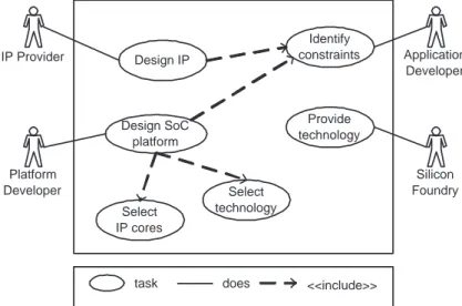
Since design effort remains constant across market changes, while time-to-market pressures demand rapid development, design-reuse is key for protecting investments [6]. Figure 1.1 illustrates trends of design-reuse for SoC-PE. Projec-tions show that in 2020 only 10 % of a new SoC will be designed from scratch. The elementary SoC component, also known as macrocell or Intellectual Property (IP) core, is designed in such a way that it can be easily integrated in a variety of products. ASIC design, once carried on by a single team, is now the result of a combined effort between IP core providers and SoC integrators. Figure 1.2 shows with a UML-like use-case notation the different actors taking part into the SoC development process. While the picture represents them as separate entities, big semiconductor companies cover more than one task in the development flow.
1.2. Design once, Reuse many
To manage the billions of transistors complexity of today’s SoCs, designers use a divide-and-conquer approach, assembling pre-designed and pre-verified IP cores. The IP market received a significant boost in recent years and it features core of different kinds and flavors [7].
This file is an extract of the whole work.
1.2 Design once, Reuse many
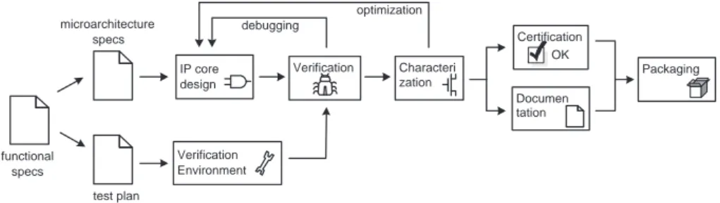
functional specs microarchitecture specs test plan IP core design Verification debugging Characteri zation optimization Certification OK Documen tation Packaging Verification Environment
Figure 1.3.: IP core development cycle
Hard macrocells are technology dependent cores fully designed, placed, and routed by the IP supplier on a given technology and delivered to the SoC in-tegrator as a GDSII file. Examples of hard macrocells are memories, I/O pe-ripherals (USB, ethernet, etc.) and mixed-signal or analog components such as DACs, ADCs, PLLs and others. However, because of dependency from technol-ogy, hard macros are distributed in small markets and thus provide low return on investments.
Actually, the IP core market is dominated by soft cores. Soft cores are technol-ogy independent macrocells that are customized for a specific foundry process by means of Electronic Design Automation (EDA) tools. Technology independence ensures reuse of core with several technology libraries, including FPGA devices. Only digital designs can become soft cores, because the use of abstraction layers detaches technology aspects from design functionality (see Section 1.4).
The IP core development cycle is illustrated in Figure 1.3. All reusable IPs, either hard or soft, retain a set of fundamental characteristics [8]:
designed for use in multiple technologies : while this is implicit for soft macro-cells, for hard macrocells this means having an effective porting strategy for mapping the core onto new technologies;
independent from toolchain : integration of core should not depend on any EDA tool vendor, since SoC integration flow is not standardized and it changes between design centers;
verified and certified as stand-alone unit : the core should be fully verified be-fore any integration takes place; the verification phase should be certified by means of consistent metrics such as code and functional coverage; fully documented : valid and illegal configurations should be clearly documented;
use cases of the core should be provided as reference for core integration; interfacing requirements should be also reported;
System-on-Chip: Concept and Trends
provided with standard interfaces : the core should be connected to the SoC through well defined interfaces. Although there is no formal standard for on-chip interfaces, de facto standards exist like the AMBA protocols set (APB, AHB, AXI) developed by ARM, the OCP specification, proposed by the OCP-IP Consortium, STbus by STMicroelectronics and CoreConnect from IBM.
To address the complex trade-offs which occur during SoC design, several works in literature suggest to decouple central aspects of the design, such that they can be optimized independently from each other; this approach is known as orthogo-nalization of concerns and is at the basis of platform based design [9].
For IP design, computation and communication aspects are separated when a socket based approach is adopted. With this approach, IP core functionality is implemented independently from interconnect properties (i.e. protocol, latency, bandwidth). All interconnect-related stuff is relegated to the IP socket, which can be fine-tuned to the interconnect without affecting the rest of the design.
Socket based design principles are taken to a greatest extent in the Network-on-Chip design paradigm, where cores are connected to the communication in-frastructure in a Plug & Play fashion (see Chapter 5 for details).
1.3. SoC Digital Building Blocks
As already pointed out in previous sections, an SoC should be flexible enough to be employed in more than one product. An SoC platform is assembled using both application specific and software programmable cores, where the former are committed once and for all to a given functionality, while the latter can be instructed at run-time to implement one among several functionalities.
Flexibility is directly related to the amount of software programmable cores populating the platform, however performance favors application specific cores, due to their superior timing and power consumption figures. The right SoC platform is thus a trade-off choice between flexibility and performance driven by application constraints.
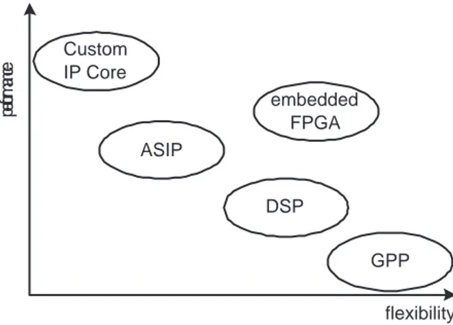
Providing an in-depth description on how to design effective platforms is out of the scope of this thesis. This section classifies platform building blocks according to their flexibility and illustrates their advantages and drawbacks. Figure 1.4 proposes a qualitative comparison of SoC components with respect to the perfor-mance/flexibility trade-off.
Application Specific IP Core
This class of core represents for SoCs what ASICs were for Systems-on-Board in late 80’s: a system component tailored to a very specific function (e.g. Fourier
This file is an extract of the whole work.
1.3 SoC Digital Building Blocks
flexibility pe rform an ce Custom IP Core embedded FPGA DSP GPP ASIP
Figure 1.4.: Comparison of SoC digital building blocks
Transform), and thus optimized for best timing, power consumption and area oc-cupation performance. Application Specific IP Cores are selected each time the target application imposes hard constraints on some system metric (i.e. through-put, latency, etc.) and software programmable cores requires unacceptable over-heads, such as power consumption in SoC-PE.
Today, application specific IP cores are experiencing a noticeable growth of the synthesis-time configuration space. Although core functionality is static once in silicon, the SoC integrator can fine tune an ever increasing number of parame-ters during implementation to match his needs. From the IP provider point of view, extreme IP flexibility guarantees the reuse in the largest possible number of applications. Building blocks for on-chip communication infrastructures are a good example of IP cores requiring extensive configuration capabilities.
Digital Signal Processor
A Digital Signal Processor (DSP) is a software programmable core designed to elaborate highly regular algorithms, such as signal processing ones, with real-time requirements up to few Msample/s. High-end DSP cores and entry-level ones might differ for the number of computational units or the number of buses, but will retain a common set of features listed hereafter:
Harvard architecture : program and application data are exchanged between central memory and computational units through dedicated and indepen-dent buses, this way instruction fetch does not affect system bandwidth;
System-on-Chip: Concept and Trends
VLIW instruction set : Very Long Instruction Word (VLIW) approach is a form of instruction level parallelism; the DSP controls multiple computational units at the same time with a single instruction fetch;
single cycle execution : most DSP instructions execute in one clock cycle: this ensures high throughput execution and eases software development as la-tency can be estimated directly from (assembler) source code;
specialized ALUs : a DSP is equipped with enhanced Arithmetic Logic Unit (ALU) featuring barrel shifter and Multiply and Accumulate (MAC) op-erators; these operations are building blocks for most signal processing algorithms e.g. the MAC unit is mainly intended for FIR filters implemen-tation;
pipelined data path : computational units exchange data between them through dedicated data paths to avoid data bus congestion;
zero-overhead looping : loop exit condition is managed with no extra clock cycles;
enhanced address generator : provides indirect addressing capabilities; per-forms automatic address modification such as modulo addressing for circu-lar buffers (FIR filters) and bit-reverse addressing (FFT/IFFT algorithms); The main advantage of DSP is the possibility to develop applications using the C language, thus gaining access to a wide choice of efficient mathematical and signal processing libraries. Since the effort of exploiting algorithm parallelism is left to the compiler, the designer has not to worry about the DSP architecture and the source code can be easily retargeted to other platforms by means of source code recompilation. For this reason, an efficient compiler is a must to take fully advantage of the DSP resources.
As a major drawback, design optimization is constrained by the DSP architec-ture itself: algorithm must be re-scheduled to take into account available process-ing units and resultprocess-ing data flow not necessarily matches the original one. Data buses can either incur congestion or waste of bandwidth, as there is no way to modify bus width according to exchanged data type.
Field Programmable Gate Array
A Field Programmable Gate Array (FPGA) [10] can be seen as a fair amount of uncommitted logical and interconnect resources, programmable by the designer when the device is already inserted in the final system, that is to say on the field. FPGAs entered the SoC worlds as target prototyping platforms, but they are founding their way as SoC building blocks (embedded FPGA cores).
This file is an extract of the whole work.
1.3 SoC Digital Building Blocks
The FPGA paradigm is much more application specific than the DSP one. The designer chooses what kind of computational units implement, how they will internally work and which way they will communicate. Increased customiza-tion respect to a DSP architecture enables real-time data processing up to few Gsample/s with reasonable power consumption (hundreds of mW). Nonetheless, a DSP is an off-the-shelf architecture that must be instructed by the designer through software programming, while for FPGA the designer is responsible for committing low-level logical resources to build a dedicated architecture: one says that a FPGAs have finer, or bit-level, granularity with respect to DSPs.
Embedded FPGA cores provide SoCs with reconfigurability (Reconfigurable SoCs). The same chip area is committed to different tasks in a time multiplexed way. Technology independent application specific cores can be fully reused in this context, the limit being the total capacity of the embedded array and the level of concurrency required between tasks.
General Purpose Processor
The general purpose processor (GPP) is the most widespread platform in the market. The GPP can virtually address any application and can be programmed with a variety of low and high level languages. Its greatest drawback is the lack of optimality in terms of computational performance and power consumption which is a direct consequence of its general purpose nature. GPP cores are usually employed in SoCs for control-intensive tasks either by using or not an operating system. GPP are also used for executing power-management policies or for scheduling reconfiguration of embedded FPGAs. Examples of GPP cores are the ARM7 and ARM9 families, integrated in a high number of SoC-PE and IBM POWER Architecture derivatives, used as the controller for the eight dsp-like cores in the Cell Broadband Engine and integrated as hard macro in Xilinx Virtex FPGAs.
Application Specific Instruction Set Processor
The Application Specific Instruction Set Processor (ASIP) is a design paradigm which is halfway between ASIC and GPP: the basic idea is to decompose the ap-plication into kernel functions and then build up a processor architecture whose instruction set is based on these kernel functions. Resulting architecture is ap-plication specific, but it is also software programmable, because it must be in-structed with ad-hoc software.
It is clear that such approach could be optimal if a family of applications, rather than a single application, has to be implemented. It is also assumed that elements of the family share a common set of algorithmic features, in order to better exploit instruction set decomposition of the application. The resulting
System-on-Chip: Concept and Trends
architecture is then general purpose for the considered family of applications, but gives the user the ability to choose a specific application through simple software programming. An example of commercially available ASIPs are network processors [11].
1.4. Abstraction Layers: Complexity Under the Hood
Digital electronics is built on abstraction layers. Indeed its own definition, i.e. mapping of boolean logic levels onto voltage ranges, abstracts digital circuit de-sign by separating technology aspects (type of components, power supply voltage, noise margins, etc.) from gate functionality (AND, OR, NOT, etc.).
Generally speaking, an abstraction layer encapsulates implementation details of lower layers into design entities that are, in turn, composed into more complex designs. Composed designs are fully independent from and do not change if the underlying layers are modified. Since lower level implementation details are hidden, the design space is reduced, thus the exploration can be conducted more efficiently.
It is worth noting that, the layer is barely useful by itself if not coupled with a methodology for synthesizing lower layers starting from higher ones. Further-more, design abstraction implies degradation of the optimal solution space, since the designer loses control over abstracted features. To counterbalance this draw-back, the methodology should provide automatic or semi-automatic procedures for exploring the solution space and, even better, should be supported by opti-mization algorithms to ensure design closure with respect to user supplied con-straints.
Figure 1.5 compares the trends of digital integrated circuits complexity with the number of transistors an expert engineer can cope with in one month, that is his productivity. Complexity increases 68 % per year due to improvements in semiconductor manufacturing technologies and can be considered as an experi-mental representation of the “mythological” Moore’s Law. Increase in produc-tivity (21 %) is due to shifts in design methodologies thanks to new abstraction layers and EDA tools. The distance between the two curves is widely known in literature as the design/productivity gap. Design productivity is a concern con-tinuously and specifically addressed by the ITRS [4], since full exploitation of deep sub-micron technology nodes can be achieved only with streamlined design methodologies.
Historically, new abstraction layers and methodologies did not find industrial exploitation if the they did not provide substantial improvements over previous design approaches and consolidated best practices. A remarkable example is the Register Transfer Level (RTL) methodology based on Hardware Description Languages (HDLs), which increased designer productivity from 20 Kgates in 1986
This file is an extract of the whole work.
1.4 Abstraction Layers: Complexity Under the Hood
Co m ple xity Lo gic Tra ns isto r pe r C hip (M ) 1981 1985 1989 1993 1997 2001 2005 2009 100 1000 10 1 0.1 0.01 0.001 Pr od uc tivity (K )Tr an sisto r/Sta ff-M on th 1000 10000 100 10 1 0.1 0.01 10000 Complexity 100000 Productivty 68 %/Year 21 %/Year
Figure 1.5.: The design/productivity gap. Source: [12]
to 250 Kgates in the mid-1990 [13]. The success of the RTL methodology is due to logic synthesis tools which brought together automatic mapping of RTL code onto logic primitives and optimization of chip area and timing, i.e. design aspects which are not directly captured by the register transfer abstraction layer.
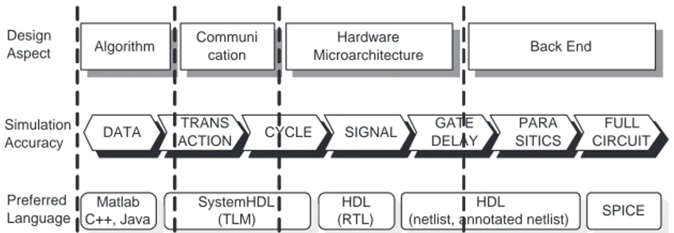
When breaking the million gates complexity barrier, verification becomes as challenging as design, up to the point that a verification-first approach is consid-ered the only viable solution to tackle the increasing costs of SoC manufacturing due to Engineering Change Order (ECO) and mask respins. By using higher levels of abstraction, specific design aspects can be verified earlier [14], limiting full-blown simulation to abstraction layers where execution speed is tolerable. Close-to-physical layers rely on regression tests with respect to reference models on static verification approaches, such as logic equivalence and Static Timing Analysis (STA). Hardware Verification Languages (HVL) can work at multiple levels of abstraction and effective verification environment are designed in such a way that verification components can be reused throughout the design cycle. Figure 1.6 is a coarse representation of abstraction layers used for designing and verifying today SoCs. Simulation accuracy varies inversely with the number of simulated gates per clock cycle. In the following a short summary for each design aspect is provided:
Algorithm : Many digital circuits implement signal processing algorithms (e.g. Discrete Fourier Transform, JPEG image compression, channel encoding and decoding, etc.). High level programming languages such as Matlab, Java or C++ are used to model algorithm data flow and finite precision arithmetic effects.
System-on-Chip: Concept and Trends
HDL (RTL) SystemHDL (TLM) Matlab C++, Java DATA TRANSACTION CYCLE SIGNAL Simulation Accuracy Design Aspect Preferred Language GATE DELAY PARA SITICS FULL CIRCUIT HDL
(netlist, annotated netlist) SPICE Algorithm Communi
cation
Hardware
Microarchitecture Back End
Figure 1.6.: Abstraction Layers in SoC design
Communication : Today SoCs are composed of several cores continuously ex-changing data. As the number of cores increase, the interconnect as well as the protocols should be carefully designed to avoid communication dead-locks which degrade single core performance. Transaction-Level Modeling (TLM) [15] is the preferred abstraction layer for exploring this design as-pect using languages such as SystemC [16], SystemVerilog [17] or bare C++. Accuracy of transaction-level simulators can be improved down to clock cycle by using timed models.
Hardware Logic : hardware behavior is defined down to the bit level. RTL is the preferred abstraction layer. Functionality is described as registers con-nected each others with boxes implementing Finite State Machines (FSMs) and boolean logic equations. Timing accuracy does not got beyond the clock cycle. Preferred languages are Verilog and VHDL.
Back-end : back-end refers to all intermediate design views between gate-level netlists and GDSII geometries, going through SPICE netlist. These views contain all design’s technology related aspects such as logic and intercon-nect delays, clock skew, effects of parasitics and so on. Verification of back-end design aspects is mainly based on static techniques. Regression tests are used to verify Design Rule Check (DRC) fixes that might occur. Full circuit simulations are rarely perfomed, unless targeted to very specific corner cases.
Abstraction is not limited to the layers described in this section. Operating systems running on GPP cores introduce further layers which extend in the soft-ware domain. Platform based design principles state that platform functionalities should be defined in such a way that the actual implementation, either hardware or software, is irrelevant to the application designer. Some authors [18] even suggest to stop calling circuits hardware, since this distinction belongs to the
This file is an extract of the whole work.
1.5 Organization of this Work
old days of transistor-level design: design patterns such as concurrency are com-mon to both world and should be treated in a consistent and unified way when designing compound platforms.
1.5. Organization of this Work
This dissertation deals with both computing and communication aspects of SoC platforms with emphasis on telecommunications and signal processing applica-tions. The focus is on hardware architectures for baseband processing, par-ticularly Low-Density Parity-Check (LDPC) channel decoders and Fast Fourier Transform (FFT) processors for multi-band modulation schemes.
LDPC codes were first introduced by Gallager in 1963 [19], but soon abandoned because their implementation complexity was far exceeding the capabilities of the microelectronic design technologies of that times. Today, the increasing de-mand of high data rate and reliability in modern communication systems is push-ing next-generation standards, such as DVB-S2, WLAN (802.11n) and WMAN (802.16e), toward error correction schemes featuring high throughput decoding at near Shannon limit performance [20]: both LDPC and Turbo codes [21] are remarkable examples of this class of error correction codes.
However, peculiarities of the LDPC decoding algorithm (iterative processing, transcendental operators, pseudo-random message exchange) strongly affect tra-ditional hardware design metrics (area, speed, power) making it difficult to meet feasible implementation requirements without spoiling communication perfor-mance [22]. To this aim, Chapter 2 presents a bit-true simulator specifically conceived for profiling LDPC communication performance under finite-precision arithmetic and sub-optimal decoding algorithms. In Chapter 3 the simulator is used to prove the effectiveness of (i) an original decoding schedule with low-memory requirements, (ii) a modified decoding schedule for high-throughput decoding, and (iii) an approximated transcendental operator for implementing LDPC computing kernels with minimum area. These results are then projected onto lower levels of abstraction presenting the implementation of a whole decoder on a 0.18 µm CMOS standard-cells library.
Chapter 4 presents an FFT/IFFT core compiler particularly suited for the hardware implementation of communication systems based on Orthogonal Fre-quency Division Multiplexing (OFDM). OFDM has been adopted in modern communication standards to provide enhanced system performance and better deployment of available bandwidth. The compiler is a toolchain made of three parts: a system-level profiler, an RTL architectural template and a codebase generator. The system-level profiler explores the design space automatically and feeds the codebase generator with configuration data for the architectural tem-plate. The accuracy-driven configuration engine minimizes operands bit-width
System-on-Chip: Concept and Trends
(and thus minimum circuit complexity) within budgets provided by the user. The flexibility and re-usability of the toolchain is demonstrated through several case studies which encompass all current state-of-the-art OFDM communications standards (WLAN, WMAN, xDSL, DVB-T/H, DAB and UWB) and top-class silicon technologies such as deep sub-micron standard-cells libraries (CMOS 65 and 90 nm) and commercially available SRAM FPGA devices implemented with 90 nm process. The implementation flow for the deep sub-micron libraries em-ploys leakage power minimization techniques mixing up library cells with different threshold voltages.
In Chapter 5 the focus shifts on communication aspects of SoC design. The Network-on-Chip (NoC) paradigm [23,24] is explained and its benefits and draw-backs discussed. NoCs takes the idea of orthogonalization of concerns to its greatest extent, by adopting ISO/OSI-like [25] abstraction layers for the design of on-chip micronetworks. Thanks to the abstraction layers (physical, data-link, network, transport, application) of the ISO/OSI stack, NoCs provide a methodol-ogy for designing an interconnect architecture independently from the attached IP cores. Design flow parallelization, scalability and reusability all benefit from this approach; furthermore, NoCs allow IP macrocells to be connected to the network in a Plug & Play fashion, which represents a powerful advantage for system-level design exploration and performance analysis thus reducing time-to-market and development costs.
Chapter 6 discusses a low-complexity link microarchitecture for reliable com-munication across mesochronous clock domains. With respect to a fully syn-chronous paradigm, in a mesosyn-chronous scheme IP macrocells are clocked by sig-nals with the same frequency but with a time-invariant phase offset. In modern SoCs, this is a consistent scenario since the clock signal is generated from a single source and distributed across the chip floorplan with a space-dependent time-invariant phase offset known as clock skew. The proposed link easily integrates in a standard-cells design flow without requiring special custom components or any specific EDA tool.
Chapter 7 presents advanced and innovative techniques for streamlining the design and the configuration of building blocks for NoC platforms. A novel methodology, named metacoding, is used for generating correct-by-construction technology independent RTL codebases. Metacoding is exemplified with the building blocks of the STMicroelectronics Spidergon Network-on-Chip intercon-nect, jointly developed with the Advanced System Technology Laboratories of STMicroelectronics Grenoble, France.
Chapter 8 summarizes the contribution and main results of this thesis and provides indications on future research activities.
Chapter 8.
Conclusions
This dissertation proposed engineering solutions to compelling design aspects of SoC for telecommunications and signal processing. Problems have been tackled at different levels of abstraction, from algorithm down to gate-level synthesis, to guarantee low complexity hardware implementation with top-class system level performance. Design reuse and automation have been a primary concern through-out the work, being key factors to keep the fast pace of semiconductor industry. All proposed solutions have been evaluated from the hardware complexity point of view, considering standard-cells libraries on three CMOS technology nodes: 0.18 µm, 90 nm and 65 nm. The characterization took into into account critical problems of deep submicron technologies like leakage power minimization. The design flow developed during this thesis can manage multi-Vt libraries at 90 and 65 nm and is ready-to-go on 45 nm standard-cells libraries.
8.1. Algorithms and Architectures for LDPC
Decoders
The hardware design of an LDPC decoder is a challenging task, due to the strong non-linear interactions existing among the variables of the design space: BER per-formance, code structure, decoding throughput and latency, number of iterations, architectural parallelism, approximation of CN processing, hardware complexity (timing, area and power). In this respect the novel solutions discussed in this dissertation have been co-designed at the algorithmic and the architectural level. Regarding approximations of CN functions, a ultra low complexity approx-imation named P -output decoding was proposed. P -output decoding reduces the messages computed by the CN processor to only P + 1 different values and employs a Modified Min-Sum algorithm. The approximation demonstrated no appreciable loss in performance compared to the exact message passing algo-rithm, even with P = 1. Using only 5 bits for representing extrinsic messages, the IL is below 0.2 dB down to BER of 10−8.
This file is an extract of the whole work.
8.1 Algorithms and Architectures for LDPC Decoders
Logic synthesis on 0.18 µm CMOS technology showed that the proposed ar-chitecture compares favorably with other state-of-the-art implementations. De-pending on the code in use, the VNP can even dominate the complexity of the whole decoder. For instance, this is the case of a decoder for DVB-S2, where the adoption of the approximation described here would save about 59% of the com-plexity of the node processors (VN and CN, together) declared by other works in literature.
Single phase decoding schedules short the iteration time, thus doubling the decoding throughput of belief propagation, or halving the clock frequency if throughput is not a primary concern for the target application. In this respect, the layered decoding schedules, widely treated in literature, was extended and generalized to “non-layered” codes and a new decoding schedules, named adap-tive single phase decoding, was proposed.
Non-layered codes are those structured LDPC codes whose parity-check matrix does not allow support of layered decoding in time-multiplexed architectures, unless a layer width of one row is chosen, which is impractical for any given application.
Starting from the original formulation, the rearrangement of the decoding oper-ations led to specify two different but similar architectures, one directly producing the new estimate of the soft output (SO-based decoding), the other computing its incremental variation with respect to the previous estimate (δ-based decoding). Although the former is suitable for true layered codes, it can be also used with non-layered codes when the last update of the SO in common overwrites previ-ous in-layer updates. On the other hand, the second architecture exploits all the contributes of a certain layer to the shared SO, by summing deltas together.
For profiling purpose, a metric η was defined for measuring how much a struc-tured code is non-layered (ratio of overlapping blocks over total number of blocks). The δ mechanism exhibited an IL smaller than 0.05 dB with η up to 34%. At the same time, the average number of iterations is one half that of a flooding decoder. Reordering the sequence of layers further relaxes the problem by minimizing η: in this case, the same speed of exact layered is achieved. Conversely, SO-based approximation suffers from impairments in the BER of about 0.1 dB, and must rely on layers reordering to support high-speed decoding.
Logic synthesis on 0.18 µm CMOS technology showed that the complexity over-head of the ancillary circuitry to perform layered decoding is about 22-24% of the original check node processor, while the overall saving for not implementing the variable node processor is about 41-43% in terms of area and power consumption. Adaptive Single Phase Decoding adaptively updates a single metric for each variable node in the codeword, by means of a single-phase processor fed with the channel a priori LLRs. The single-phase processor outputs refined approxima-tions of the SO in the transmitted codeword, which are continuously cumulated
Conclusions
to the node metric in a running sum with leakage. This makes the proposed solution very attractive from the performance-complexity trade-off point of view: for a reduction of the message memory of about 70-80% and of chip complexity of about 12%, only few tenths of dB are paid in the transmission SNR with respect to the traditional message passing decoding.
8.2. Processing Core for OFDM transceivers
Chapter 4 presented an automated environment for fast design space exploration and automatic generation of low-complexity stream-oriented FFT/IFFT IP cores in the context of VLSI implementation of OFDM systems. A custom software tool has been developed to explore the design space at system level using either open or closed-loop analysis. The software profiles FFT numerical accuracy with respect to three arithmetic approaches (fixed-point, BFP and CBFP) by means of Monte Carlo simulations. In closed-loop analysis, the internal arithmetic is automatically configured to minimize data bit-widths within the SQNR budget specified by the user.
The arithmetic configuration is used to generate a VHDL database starting from a fully configurable RTL macrocell featuring:
• fully-pipelined radix-4 cascade architecture with optional radix-2 stage for power-of-two FFT/IFFT lengths;
• FFT length programmable at run-time for multi mode systems such as xDSL, DVB-T/H or WLAN;
• both FFT/IFFT operations implemented in the same core for half-duplex transceiver (e.g. WLAN and UWB);
• maximum throughput of 1 complex sample/cycle with controllable pipeline (freeze/flush);
• support for three types of internal arithmetics for optimal trade-off between hardware complexity and numerical accuracy.
The effectiveness of the tool has been proved by configuring and generating several IFFT/FFT cores each dedicated to multi-band OFDM modulation and demodulation in a different communication standard: WLAN, WMAN, xDSL, DVB-T/H, DAB and UWB. The test cases covered a wide design space in terms of transform length (64 to 8192), throughput (8 to 528 Msample/s) and processing accuracy (SQNR from 29 to 94 dB).
The generated FFT/IFFT cores have been synthesized and characterized on a 65 nm CMOS technology with multi-Vt library versions. The same cores have also
This file is an extract of the whole work.
8.3 Network-on-Chip Components
been synthesized on SRAM-based FPGA devices and 90 nm CMOS standard-cells library to demonstrate ease of re-targeting and to compare power figures between different implementation technologies. Synthesis results showed a low complexity in terms of gate count and RAM/ROM bits when compared with other works in recent literature that consider the same system level performance (throughput, transform sizes and numerical accuracy).
8.3. Network-on-Chip Components
Network-on-Chip is a new paradigm for designing scalable and reusable on-chip interconnection networks that will eventually replace traditional shared-bus in-terconnects. This thesis considered issues related to the design and the imple-mentation of the building blocks of a NoC platform: link, router and network interface.
Chapter 6 proposed a mesochronous physical link micro architecture named SIM-L. The mesochronous paradigm is a way to model fully synchronous systems affected by clock skew issues, which are limiting timing performance of today fully synchronous systems. SIM-L enables skew constraint looseness in the clock tree synthesis, frequency speed-up, power consumption reduction and faster back-end turnarounds. With respect to the state of the art, SIM-L architecture can be easily integrated in a conventional digital design flow since it is implemented by means of standard cells.
Experiments on a 65 nm CMOS standard-cells library demonstrated a maxi-mum operating frequency of 1 GHz by using only low-leakage cells. SIM-L has been also integrated in an eight-tile MPSoC based on the STMicroelectronics Spidergon platform, featuring eight routers and eight NIs using 72 bit wide data packet bus. In this test-case SIM-L exhibited area and leakage penalties of only 3% and 0.5% respectively vs. NoC components.
A patent application for SIM-L architecture has been filed in both Europe and the United States.
Chapter 7 discussed the implementation of a router for hierarchical networks based on Spidergon-like topologies. To cope with the extremely wide configura-tion space, a new methodology, named metacoding, was proposed for generating correct-by-construction technology independent RTL codebases. The RTL coding itself is abstracted and modeled with an Object Oriented framework, integrated within a commercial tool for IP packaging (Synopsys CoreTools suite).
Compared with traditional coding styles based on pre-processor directives, the proposed methodology produced 65% smaller codebases and reduced the config-urations to verify of three orders of magnitude. Similar techniques have also been applied to the design of the network interface. Particularly, metacoding gener-ated the HDL files describing the whole set of network features: network and
Conclusions
transport packet formats, routing and QoS tables, network access policy. The approach ensured consistency among all instances of network components and re-duced harmful mismatches between the configuration and the verification phases by generating configuration files for the verification environment. The whole set of metacoding plug-ins has been integrated in the proprietary STMicroelectronics system level flow for generating NoC platforms.
Bibliography
[1] T. Halfhill, “The Mythology of Moore’s Law,” IEEE Solid-State Circuits Society Newsletter, vol. 20, no. 3, pp. 21–25, Sept. 2006.
[2] G. Moore, “Cramming more components onto integrated circuits,” Elec-tronics, vol. 38, no. 8, p. 114 ff., April 1965.
[3] ——, “Progress in digital integrated electronics,” in International Electron Devices Meeting. IEEE, 1975, pp. 11–13.
[4] International Technology Roadmap for Semiconductors. [Online]. Avail-able: www.itrs.net
[5] Feng, Wu-chun and K. Cameron, “The green500 list: Encouraging sustain-able supercomputing,” Computer, vol. 40, no. 12, pp. 50–55, 2007.
[6] R. Saleh, S. Wilton, S. Mirabbasi, A. Hu, M. Greenstreet, G. Lemieux, P. Pande, C. Grecu, and A. Ivanov, “System-on-chip: Reuse and integra-tion,” Proc. IEEE, vol. 94, no. 6, pp. 1050–1069, 2006.
[7] M. Jacome and H. Peixoto, “A survey of digital design reuse,” IEEE Des. Test. Comput., vol. 18, no. 3, pp. 98–107, 2001.
[8] M. Keating and P. Bricaud, Reuse Methodology Manual for System-On-A-Chip Designs. Springer-Verlag, 2002.
[9] K. Keutzer, A. Newton, J. Rabaey, and A. Sangiovanni-Vincentelli, “System-level design: orthogonalization of concerns and platform-based design,” IEEE Trans. Comput.-Aided Design Integr. Circuits Syst., vol. 19, no. 12, pp. 1523–1543, Dec 2000.
[10] S. Trimberger, Ed., Field-programmable gate array technology. Kluwer Academic Press, 1994.
[11] Products for communication from Intel. [Online]. Available: www.intel. com/netcomms
[12] SEMATECH: Accelerating the next technology revolution. [Online]. Available: www.sematech.org/
This file is an extract of the whole work.
Bibliography
[13] M. Santarini. (2000) RTL: advanced by three companies. EETimes. [Online]. Available: www.eetimes.com/
[14] P. Rashinkar, P. Paterson, and L. Singh, SystemonaChip Verification -Methodology and Techniques. Springer-Verlag, 2000.
[15] F. Ghenassia, Ed., Transaction-Level Modeling with SystemC: TLM Con-cepts and Applications for Embedded Systems. Springer, 2005.
[16] IEEE Standard SystemC Language Reference Manual, 1666, IEEE Com-puter Society Std., 2005.
[17] SystemVerilog. [Online]. Available: www.systemverilog.org
[18] F. Vahid, “It’s time to stop calling circuits hardware,” Computer, vol. 40, no. 09, pp. 106–108, 2007.
[19] R. Gallager, “Low-Density Parity-Check Codes,” Ph.D. dissertation, Mas-sachusetts Institutes of Technology, 1960.
[20] C. E. Shannon, “A mathematical theory of communication,” Bell System Technical Journal, vol. 27, pp. 379–423, 623–656, 1948.
[21] C. Berrou, A. Glavieux, and P. Thitimajshima, “Near shannon limit error-correcting coding and decoding: Turbo-codes,” in IEEE International Con-ference on Communications, vol. 2, may 1993, pp. 1064–1070.
[22] T. Brack, F. Kienle, and N. Wehn, “Disclosing the LDPC Code Decoder De-sign Space,” in Proc. 2006 DeDe-sign, Automation and Test in Europe (DATE ’06), Munich, Germany, mar 2006.
[23] W. Dally and B. Towles, “Route packets, not wires: on-chip interconnection networks,” in Proc. Design Automation Conference (DAC), 2001, pp. 684– 689.
[24] L. Benini and G. De Micheli, “Networks on chips: a new SoC paradigm,” IEEE Computer, vol. 35, no. 1, pp. 70–78, Jan. 2002.
[25] H. Zimmermann, “OSI reference model–the ISO model of architecture for open systems interconnection,” IEEE Trans. Commun., vol. 28, no. 4, pp. 425–432, April 1980.
[26] D. MacKay and R. Neal, “Good codes based on very sparse matrices,” in 5th IMA Conference on Cryptography and Coding, Springer-Verlag, Ed., 1995, pp. 100–111.
Bibliography
[27] A. Blanksby and C. Howland, “A 690-mW 1-Gb/s 1024-b, rate-1/2 low-density parity-check code decoder,” IEEE J. Solid-State Circuits, vol. 37, no. 3, pp. 404–412, mar 2002.
[28] P. Ciao, G. Colavolpe, and L. Fanucci, “A parallel VLSI architecture for 1-Gb/s, 2048-b, rate-1/2 Turbo Gallager code decoder,” in Euromicro Sym-posium on Digital System Design (DSD), aug 2004, pp. 174–181.
[29] M. Mansour and N. R. Shanbhag, “High-throughput LDPC decoders,” IEEE Trans. VLSI Syst., vol. 11, no. 6, pp. 976–996, Dec 2003.
[30] H. Zhong and T. Zhang, “Block-LDPC: A Practical LDPC Coding System Design Approach,” IEEE Trans. Circuits Syst. I, vol. 52, no. 4, pp. 766–775, Apr 2005.
[31] M. Fossorier, M. Mihaljevic, and H. Imai, “Reduced complexity iterative decoding of low-density parity check codes based on belief propagation,” IEEE Trans. Commun., vol. 47, no. 5, pp. 673–680, may 1999.
[32] M. Rovini, F. Rossi, N. L’Insalata, and L. Fanucci, “High-Precision LDPC Codes Decoding at the Lowest Complexity,” in Proc. 14th European Signal Processing Conference (EUSIPCO), Sept. 2006, p. (to appear).
[33] M. Rovini, “Low-density parity-check codes: A tutorial,” ESA/ESTEC, Scientific and Technical Report STR-245, May 2004.
[34] F. Zarkeshvari and A. Banihashemi, “On implementation of min-sum algo-rithm for decoding low-density parity-check (LDPC) codes,” in Proc. IEEE GLOBECOM, vol. 2, Nov 2002, pp. 1349–1353.
[35] F. Guilloud, E. Boutillon, and J. Danger, “λ-Min Decoding Algorithm of Regular and Irregular LDPC Codes,” in Proc. 3nd International Sympo-sium on Turbo Codes & Related Topics, Brest, France, sep 2003, pp. 451– 454.
[36] R. Tanner, “A recursive approach to low complexity codes,” IEEE Trans. Inf. Theory, vol. 27, no. 5, pp. 533–547, Sep 1981.
[37] F. Kschischang, B. Frey, and H.-A. Loeliger, “Factor graphs and the sum-product algorithm,” IEEE Trans. Inf. Theory, vol. 47, no. 2, pp. 498–519, Feb 2001.
[38] D. MacKay, “Good error-correcting codes based on very sparse matrices,” IEEE Trans. Inf. Theory, vol. 45, no. 2, pp. 399–431, Mar 1999.
This file is an extract of the whole work.
Bibliography
[39] H. Michel, A. Worm, and N. Wehn, “Influence of quantization on the bit-error performance of turbo-decoders,” in Proc. VST Spring, vol. 1, May 2000, pp. 581–585.
[40] “IEEE P802.11 Wireless LANs WWiSE Proposal: High throughput exten-sion to the 802.11 Standard,” August 2004, IEEE 11-04-0886-00-000n. [41] C. L. David MacKay’s Research group. Encyclopedia of Sparse Graph
Codes. [Online]. Available: http://www.inference.phy.cam.ac.uk/mackay/ [42] T. Zhang, Z. Wang, and K. Parhi, “On finite precision implementation of
low density parity check codes decoder,” in Proc. IEEE ISCAS, vol. 4, May 2001, pp. 202–205.
[43] H. Michel and N. Wehn, “Turbo-decoder quantization for UMTS,” IEEE Commun. Lett., vol. 5, no. 2, pp. 55–57, Feb 2001.
[44] X.-Y. Hu, E. Eleftheriou, D.-M. Arnold, and A. Dholakia, “Efficient im-plementations of the sum-product algorithm for decoding LDPC codes,” in Proc. IEEE GLOBECOM, vol. 2, nov 2001, pp. 1036–1036E.
[45] E. Eleftheriou, T. Mittelholzer, and A. Dholakia, “Reduced-complexity de-coding algorithm for low-density parity-check codes,” Electronics Letters, vol. 37, no. 2, pp. 102–104, Jan. 2001.
[46] M. Mansour and N. Shanbhag, “Low-power VLSI decoder architectures for LDPC codes,” in International Symposium on Low Power Electronics and Design, Aug 2002, pp. 284–289.
[47] C. Jones, E. Valles, M. Smith, and J. Villasenor, “Approximate-MIN Con-straint Node Updating for LDPC Code Decoding,” in IEEE Military Com-munications Conference (MILCOM), vol. 1, Oct 2003, pp. 157–162. [48] D. Hocevar, “A Reduced Complexity Decoder Architecture via Layered
De-coding of LDPC Codes,” in IEEE Workshop on Signal Processing Systems, SISP 2004, 2004, pp. 107–112.
[49] E. Sharon, S. Litsyn, and J. Goldberger, “An Efficient Message-Passing Schedule for LDPC Decoding,” in 23rd IEEE Convention of Electrical and Electronics Engineering in Israel, Sep 2004, pp. 223–226.
[50] H. Kfir and I. Kanter, “Parallel versus sequential updating for belief prop-agation decoding,” Physica A Statistical Mechanics and its Applications, vol. 330, pp. 259–270, Dec. 2003.
Bibliography
[51] J. Zhang and M. Fossorier, “Shuffled Belief Propagation Decoding,” in 36th Asilomar Conference on Signals, Systems and Computers, Nov 2002. [52] E. Yeo, P. Pakzad, B. Nikolic, and V. Anantharam, “High Throughput
Low-Density Parity-Check Decoder Architectures,” in IEEE Global Telecommu-nications Conference, vol. 5, Nov 2001, pp. 3019–3024.
[53] H. Zhong and T. Zhang, “Design of VLSI implementation-oriented LDPC codes,” in International Symposium on Low Power Electronics and Design, vol. 1, Oct 2003, pp. 670–673.
[54] T. Richardson and V. Novichkov, “Methods and apparatus for decoding LDPC codes,” US Patent App. US2003-0033575, Feb 2003.
[55] A. Vila Casado, W. W., and R. Wesel, “Multiple rate low-density parity-check codes with constant block length,” in Asilomar Conf. on Signals, Systems and Computers, vol. 2, Nov 2004, pp. 2010–2014.
[56] F. Kienle, T. Brack, and N. Wehn, “A synthesizable IP core for DVB-S2 LDPC code decoding,” in Design, Automation and Test in Europe (DATE), 2005, pp. 100–105.
[57] M. Rovini, N. L’Insalata, F. Rossi, and L. Fanucci, “VLSI Design of a High-Throughput Multi-Rate Decoder for Structured LDPC Codes,” in Proc. 8th Euromicro Conference on Digital System Design (DSD), Aug-Sept. 2005, pp. 202–209.
[58] DIOPSIS 740 dual-core DSP, 7001A-DPS-09/04, Atmel Corporation, 2004. [59] TMS320DM644x Processors Video Benchmarks, SPRT379A, Texas
Instru-ments Inc., 2006.
[60] G. Bi and E. Jones, “A pipelined FFT processor for word-sequential data,” IEEE Trans. Acoust., Speech, Signal Process., vol. 37, no. 12, pp. 1982– 1985, 1988.
[61] T. Sansaloni, A. Perez-Pascual, V. Torres, and J. Valls, “Efficient pipeline FFT processors for WLAN MIMO-OFDM systems,” Electronics Letters, vol. 41, pp. 1043–1044, sep 2005.
[62] S. He and M. Torkelson, “A new approach to pipeline FFT processor,” in Proc. 10th International Parallel Processing Symposium (IPPS), apr 1996, pp. 766–770.
This file is an extract of the whole work.
Bibliography
[63] J. Ding, J. McCanny, and Y. Hu, “Rapid design of application specific FFT cores,” IEEE Trans. Acoust., Speech, Signal Process., vol. 47, no. 5, pp. 1371–1381, may 1999.
[64] Chua-Chin Wang, Jian-Ming Huang, and Hsian-Chang Cheng, “A 2K/8K mode small-area FFT processor for OFDM demodulation of DVB-T re-ceivers,” IEEE Trans. Consum. Electron., vol. 51, no. 1, pp. 28–32, Feb. 2005.
[65] G. Nordin, P. Milder, J. Hoe, and M. Puschel, “Automatic generation of customized discrete fourier transform IPs,” in Design Automation Confer-ence (DAC), jun 2005, pp. 471–474.
[66] A. Cortes, I. Velez, J. Sevillano, and A. Irizar, “An FFT core for DVB-T/DVB-H receivers,” in Proc. Third IEEE International Conference on Electronics, Circuits, and Systems (ICECS), vol. 1, dec 2006, pp. 102–105. [67] A. Cort´es, I. V´elez, J. Sevillano, and A. Irizar, “An approach to simplify the design of IFFT/FFT cores for OFDM systems,” IEEE Trans. Consum. Electron., vol. 52, no. 1, pp. 26–32, feb 2006.
[68] CoreFFT Fast Fourier Transform Generator, 3rd ed., Actel Inc., Dec. 2005. [69] L. Fanucci, M. Forliti, and P. Terreni, “FAST: FFT ASIC automated syn-thesis,” Integration, the VLSI Journal, vol. 33, no. 1-2, pp. 23–37, dec 2002.
[70] S. Saponara, L. Serafini, L. Fanucci, and P. Terreni, “Automated design of FFT/IFFT processors for advanced telecom applications,” in Proc. In-ternational Symposium on Signals, Circuits and Systems (SCS), vol. 1, jul 2005, pp. 103–106.
[71] J. Proakis and D. Manolakis, Digital signal processing: principles, algo-rithms, and applications. Prentice-Hall, 1996.
[72] S. Prakash and V. Rao, “Fixed-point error analysis of radix-4 FFT,” SIG-NAL PROC., vol. 3, no. 2, pp. 123–133, 1981.
[73] P. Duhamel and M. Vetterli, “Fast fourier transforms: a tutorial review and a state of the art,” Signal Process., vol. 19, no. 4, pp. 259–299, 1990. [74] R. Sherratt and Sou Makino, “Numerical precision requirements on the
multiband ultra-wideband system for practical consumer electronic de-vices,” IEEE Trans. Consum. Electron., vol. 51, no. 2, pp. 386–392, may 2005.
Bibliography
[75] C. Hui, T. J. Ding, J. McCanny, and R. Woods, “Error analysis of FFT architectures for digital video applications,” in Proc. Third IEEE Interna-tional Conference on Electronics, Circuits, and Systems (ICECS), vol. 2, oct 1996, pp. 820–823.
[76] N. Weste and D. Skellern, “VLSI for OFDM,” IEEE Commun. Mag., vol. 36, no. 10, pp. 127–131, oct 1998.
[77] L. Fanucci and M. Rovini, “A low-complexity and high-resolution algorithm for the magnitude approximation of complex numbers,” IEICE Trans. on Fundamentals, vol. E85-A, no. 7, pp. 651–654, Jul. 2002.
[78] B. Farahani and M. Ismail, “Adaptive Sigma Delta ADC for WiMAX fixed point wireless applications,” in Circuits and Systems, 2005. 48th Midwest Symposium on, aug 2005, pp. 692–695.
[79] L. Benini, G. De Micheli, and E. Macii, “Designing low-power circuits: practical recipes,” IEEE Circuits Syst. Mag., vol. 1, pp. 6–25, 2001. [80] (2006, dec) Xilinx press release 06118. [Online]. Available: www.xilinx.
com/company/press/index.htm
[81] R. Sherratt, O. Cadenas, and N. Goswami, “A low clock frequency FFT core implementation for multiband full-rate ultra-wideband (UWB) re-ceivers,” IEEE Trans. Consum. Electron., vol. 51, no. 3, pp. 798–802, 2005. [82] J. Lee, J. Moon, K. Heo, M. Sunwoo, S. Oh, and I. Kim, “Implementation of application-specific DSP for OFDM systems,” in Proc. IEEE International Conference on Circuits and Systems (ISCAS), vol. 3, may 2004, pp. 665– 668.
[83] R. Ho, K. Mai, and M. Horowitz, “The future of wires,” Proc. IEEE, vol. 89, no. 4, pp. 490–504, April 2001.
[84] A. Jantsch and H. Tenhunen, Eds., Networks on Chip. Kluwer Academic Publishers, 2003.
[85] M. Coppola, R. Locatelli, G. Maruccia, L. Pieralisi, and A. Scandurra, “Spi-dergon: a novel on-chip communication network,” in Proc. International Symposium on System-on-Chip, Nov. 2004, p. 15.
[86] L. Bononi and N. Concer, “Simulation and analysis of network on chip architectures: ring, spidergon and 2D mesh,” in Proc. Design, Automation and Test in Europe (DATE), Mar. 2006, pp. 167 – 172.
This file is an extract of the whole work.
Bibliography
[87] T. Bjerregaard and J. Sparso, “A router architecture for connection-oriented service guarantees in the MANGO clockless network-on-chip,” in Proc. Design, Automation and Test in Europe (DATE), vol. 2, Mar. 2005, pp. 1226–1231.
[88] K. Goossens, J. Dielissen, and A. Radulescu, “AEthereal network on chip: concepts, architectures, and implementations,” IEEE Des. Test. Comput., vol. 22, no. 5, pp. 414–421, Sept.–Oct. 2005.
[89] P. Martin, “Network on chip: The future of SoC power management,” in CDNLive! EMEA Conference Proceedings, 2006.
[90] SonicsMX SMART Interconnect Data Sheet, Sonics Inc.
[91] D. Wiklund and D. Liu, “SoCBUS: switched network on chip for hard real time embedded systems,” in Proc. International Parallel and Distributed Processing Symposium, April 2003.
[92] A. Pullini, F. Angiolini, P. Meloni, D. Atienza, S. Murali, L. Raffo, G. De Micheli, and L. Benini, “NoC design and implementation in 65nm technology,” in Proc. First International Symposium on Networks-on-Chip (NOCS), May 2007, pp. 273–282.
[93] S. Stergiou, F. Angiolini, S. Carta, L. Raffo, D. Bertozzi, and G. De Micheli, “×pipes lite: a synthesis oriented design library for networks on chips,” in Proc. Design, Automation and Test in Europe (DATE), vol. 2, 2005, pp. 1188–1193.
[94] D. Bertozzi and L. Benini, “Xpipes: a network-on-chip architecture for gigascale systems-on-chip,” IEEE Circuits Syst. Mag., vol. 4, no. 2, pp. 18–31, 2004.
[95] D. Messerschmitt, “Synchronization in digital system design,” IEEE J. Sel. Areas Commun., vol. 8, no. 8, pp. 1404–1419, 1990.
[96] W. Dally and J. Poulton, Digital Systems Engineering. Cambridge Uni-versity Press, 1998.
[97] J. Rabaey, A. Chandrakasan, and B. Nikolic, Digital Integrated Circuits. Prentice-Hall, 2002.
[98] A. Martin and M. Nystrom, “Asynchronous techniques for system-on-chip design,” Proc. IEEE, vol. 94, no. 6, pp. 1089–1120, June 2006.
![Figure 1.1.: SoC-PE design-reuse trends. Source: [4]](https://thumb-eu.123doks.com/thumbv2/123dokorg/7319066.89321/18.722.157.576.104.340/figure-soc-pe-design-reuse-trends-source.webp)
![Figure 1.5.: The design/productivity gap. Source: [12]](https://thumb-eu.123doks.com/thumbv2/123dokorg/7319066.89321/26.722.162.577.106.326/figure-the-design-productivity-gap-source.webp)