Università degli Studi di Ferrara
DOTTORATO DI RICERCA IN
Matematica e Informatica
CICLO XXIV
COORDINATORE Prof.ssa Ruggiero Valeria
A Scalable Parallel Architecture
with FPGA-Based Network Processor
for Scientific Computing
Settore Scientifico Disciplinare INF/01
Dottorando Tutori
Dott. Pivanti Marcello Dott. Schifano Sebastiano Fabio Dott. Simma Hubert
Contents
1 Introduction 13
2 Network Processor 19
2.1 Two-Sided Communication Protocol . . . 23
2.2 TNW Communication Protocol . . . 24
2.3 Physical Link Layer . . . 26
2.4 Torus Network Layer . . . 29
2.4.1 The “TXLINK” Module . . . 29
2.4.2 The MDIO Interface . . . 32
2.4.3 The Receiver Synchronizer . . . 33
2.4.4 The “RXLINK” Module . . . 35
2.4.5 The “Test-Bench” Module . . . 38
3 Network Processor’s CPU Interface 41 3.1 Transaction Models . . . 41
3.2 Input/Output Controller . . . 48
3.2.1 PCIe Input Controller . . . 50
3.2.2 Design Optimization, TXFIFO as Re-order Buffer . . . . 52
3.2.3 Register Access Controller . . . 53
3.2.4 DMA Engine . . . 55
3.2.5 PCIe Output Controller . . . 57
4 Software Layers 61 4.1 Communication Model . . . 62
4.2 Driver . . . 64
4.3 Low-level Library . . . 66
4.3.1 Device Initialization and Release . . . 66
4.3.2 Register Access . . . 67 3
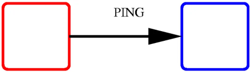
4.3.3 PPUT Send . . . 67 4.3.4 NGET Send . . . 70 4.3.5 Receive . . . 71 4.4 Application Examples . . . 72 4.4.1 Ping Example . . . 72 4.4.2 Ping-Pong Example . . . 74
5 Results and Benchmarks 77 5.1 FPGA Synthesis Report . . . 77
5.2 PHY Bit Error Rate Test . . . 77
5.3 CPU-to-NWP Transmission with PPUT Model . . . 80
5.4 CPU-to-NWP Transmission with NGET Model . . . 85
5.5 CPU-to-CPU Transmission Benchmarks . . . 92
5.5.1 Benchmarks Using libftnw . . . 92
5.5.2 Benchmarks Not Using libftnw . . . 94
5.6 Transmission Test on the AuroraScience Machine . . . 99
Scalability over multi-nodes . . . 104
6 Conclusions 109 A NWP Registers Mapping 113 A.1 RX-Link Registers . . . 113
A.2 TX-Link Registers . . . 115
A.3 TB Registers . . . 117
A.4 BAR0 and BAR1: Tx Fifos Address Space . . . 118
A.5 BAR2 Address Space . . . 120
A.5.1 TNW Register Address Space . . . 120
A.5.2 IOC Register Address Space . . . 120
A.5.3 TXFIFO Counters Registers . . . 120
A.5.4 DMA Request . . . 120
A.5.5 DMA Buffer BAR . . . 120
A.5.6 DMA Notify BAR . . . 121
B libftnw Functions Summary 125 B.1 Device Initialization and Release . . . 125
B.2 Send . . . 125
B.3 Receive . . . 127
List of Figures
2.1 Network Processor (NWP) block-diagram . . . 20
2.2 Node-to-node reliable communication diagram . . . 24
2.3 PMC-Sierra PM8358 block-diagram . . . 26
2.4 Re-partitioning example . . . 28
2.5 Torus Network (TNW) layer block-diagram . . . 30
2.6 TXLINK module block-diagram . . . 31
2.7 Management Data Input/Output (MDIO) frames diagram . . . 33
2.8 SDR and DDR scheme . . . 34
2.9 Receiver Synchronizer (RXSYNC) module block-diagram . . . . 34
2.10 RXLINK module block-diagram . . . 36
2.11 RXBUFF module block-diagram . . . 37
2.12 TB module block-diagram . . . 39
3.1 PPUT and NGET transaction-methods . . . 42
3.2 NPUT and PGET transaction-methods . . . 44
3.3 Peripheral Component Interconnect (PCI) transaction modes . . . 45
3.4 PCI Express (PCIe) memory request headers . . . 47
3.5 PCI Express (PCIe) memory completion header . . . 47
3.6 Input/Output Controller (IOC) module block-diagram . . . 49
3.7 PCI Express Input Controller (PIC) module block-diagram . . . . 50
3.8 RX_FSM block-diagram . . . 51
3.9 Re-order Buffer block-diagram . . . 53
3.10 Register Controller (RC) module block-diagram . . . 54
3.11 DMA Engine block-diagram . . . 56
3.12 POC FSM block-diagram . . . 58
4.1 NWP software stack . . . 62
4.2 VCs/memory-address mapping . . . 63 5
4.3 ftnwSend() code extract . . . 69
4.4 Ping example . . . 72
4.5 libftnw Ping code . . . 73
4.6 libftnw Ping-pong example . . . 74
4.7 ftnw Ping-pong code . . . 75
5.1 PM8354 testbed . . . 79
5.2 PM8354 BER test setup . . . 79
5.3 PPUT with Intel intrinsics . . . 82
5.4 PPUT trace without WC . . . 82
5.5 PPUT implementation with packet-level fences . . . 83
5.6 PPUT trace with WC . . . 84
5.7 PPUT trace with WC and Re-order Buffer . . . 84
5.8 Network Processor (NWP) traversal time . . . 85
5.9 Network GET (NGET) timing . . . 86
5.10 NGET latency benchmark code . . . 87
5.11 NGET latency . . . 88
5.12 NGET timing with 1 KB payload . . . 89
5.13 NGET bandwidth benchmark code . . . 90
5.14 CPU-to-CPU tx time and bw benchmark code . . . 92
5.15 PPUT and NGET CPU-to-CPU transmission time . . . 94
5.16 PPUT and NGET CPU-to-CPU bandwidth . . . 95
5.17 PPUT CPU-to-CPU tx time and bw benchmark code . . . 97
5.18 NGET CPU-to-CPU tx time and bw benchmark code . . . 98
5.19 PPUT CPU-to-CPU transmission times step . . . 100
5.20 PPUT CPU-to-CPU bandwidth with/without copy . . . 101
5.21 NGET CPU-to-CPU transmission times step . . . 102
5.22 NGET CPU-to-CPU bandwidth with/without copy . . . 103
5.23 Ping-pong test on AuroraScience concept . . . 104
5.24 Ping-pong test on AuroraScience node configuration . . . 104
5.25 Ping-pong test on AuroraScience Max Transmission time . . . 106
List of Tables
3.1 Trans. methods mapping on PCIe operations . . . 48
5.1 Network Processor (NWP) synthesis report . . . 78
5.2 PPUT bandwidth . . . 85
5.3 NGET TX time for several payload sizes . . . 89
5.4 NGET bandwidth for several payload sizes . . . 91
5.5 NGET bandwidth for several payload sizes . . . 91
5.6 PPUT bandwidth for several payload sizes . . . 93
5.7 NGET bandwidth for several payload sizes . . . 93
5.8 PPUT and NGET transmission time and bandwidth . . . 96
5.9 PPUT TX time and BW stepped . . . 96
5.10 NGET TX time and BW stepped . . . 99
5.11 Ping-pong test on AuroraScience TX time . . . 105
5.12 Ping-pong test on AuroraScience aggregate bandwidth . . . 105
A.1 BAR0 mapping . . . 119
A.2 BAR2 mapping for TNW . . . 122
A.3 BAR2 mapping for IOC . . . 123
Acronyms
ACK Acknowledge
ASIC Application Specific Integrated Circuit BAR Base Address Register
CplD Completion with Data CPU Central Processing Unit CRC Cyclic Redundancy Check
CRDBAR Credit Base Address Register CRDFIFO Credit FIFO
DATACHK Data Checker DATAGEN Data Generator DDR Double Data-Rate
DESCRFIFO Descriptor FIFO DMA Direct Memory Access DRV Device Driver
EMI ElectroMagnetic Interference FPGA Field Programmable Gate Array ID Identifier
IOC Input/Output Controller LBM Lattice Boltzmann Methods LIB Low Level Library
LID Link-ID
LVDS Low-Voltage Differential Signaling MAC Medium Access Control
MDC Management Data Clock
MDIO Management Data Input/Output MMAP Memory Mapping
MPI Message Passing Interface MRd Memory Read Request MWr Memory Write Request NAK Not Acknowledge
NTFBAR Notify Base Address Register NGET Network GET
NID Notify-ID NPUT Network PUT NWP Network Processor PCIe PCI Express
PCI Peripheral Component Interconnect PCKARB Packet Arbiter
PCKBUFFER Packet Buffer PGET Processor GET PHY Physical Layer
PIC PCI Express Input Controller PIO Programmed Input/Output PLL Phase Locked Loop
POC PCI Express Output Controller PPUT Processor PUT
RAO Remote-Address Offset RC Register Controller RCV Receiver Buffer RSND Re-send Buffer RXCLK Receive Clock
RXFSM Reception Finite State Machine RXLINK Link Receiver
RX Receive
RXSYNC Receiver Synchronizer SDR Single Data-Rate
TB Test-Bench
TLP Transaction Layer Packet TNW Torus Network
TXCLK Transmit Clock TXFIFO Injection Buffer
TXFSM Transmission Finite State Machine TXLINK Link Transmitter
TX Transmit
VCID Virtual Channel ID VC Virtual Channel
VHSIC Very High Speed Integrated Circuits WCB Write Combining Buffer
WC Write Combining
XAUI 10 GigaBit Attachment Unit Interface XGMII 10 GigaBit Media Independent Interface
Chapter 1
Introduction
Several problems in scientific computing require surprisingly large computing power which current HPC commercial systems cannot deliver. In these cases the development of application-driven machines has to be taken into account since it can be the only viable and rewarding approach.
From the computational point of view, one of the most challenging scien-tific areas is the Lattice Quantum Chromodynamics (LQCD), the discretized and computer-friendly version of Quantum Chromodynamics (QCD). QCD is the fun-damental quantum theory of strong interactions. It describes the behavior of the elementary constituents of matter (the quarks) that are building blocks of stable elementary particles, such as the proton and the neutron, and of a wealth of other particles studied in high-energy physics experiments.
Monte Carlo simulations are a key technique to compute quantitative predic-tions from LQCD. In LQCD the physical space-time is discretized on a finite 4D lattice (state-of-the-art sizes are ≈ 804lattice sites). Larger lattices would be
wel-come, since more accurate prediction would be possible. However algorithmic complexity grows with the 6th . . . 10th power of the linear lattice size, so the size of the lattices is in fact limited by available computing power.
The Monte Carlo algorithms used in this field are characterized by a very small set of kernel functions that dominate the computational load. Five or six key critical kernels correspond to ≃ 95% of the computational load. Within this already small set of kernels, the evaluation of the product of the Dirac operator, a sparse and regular complex-valued matrix, with appropriate state-vector is truly dominant, so approximately 60 . . . 90% of the computing time of LQCD codes is spent in just this task.
The Monte Carlo algorithms applied in this field (and the Dirac-operator in 13
particular) have many features that make an efficient implementation on massively-parallel machines relatively easy to achieve.
• the computation can be easily partitioned among many processors; basically the whole lattice can be divided in smaller equally-sized sub-lattices and each one can be assigned to a different CPU;
• Single Instruction Multiple Data (SIMD) parallelism can be easily exploited; all CPUs perform the same program on a different data set;
• Data access patterns of each CPU to its local memory are regular and pre-dictable, allowing to exploit data-prefetch to prevent stalls of the processors; • The communication pattern among CPUs is very simple: if processors are assigned at the vertices of a D-dimensional grid, all data communications for the Dirac kernel occur between nearest-neighbor processing elements. This suggests to use a D-dimensional mesh interconnection network, for which it is possible to obtain scalability, high bandwidth and low latency. The properties of the network are relevant for the overall performance of the program execution, since latencies and low-transfer data rate may negatively af-fect the execution time, causing stalls of the CPUs. The required features of the interconnection network are strictly related to parameters of the application, per-formance of the processor, memory bandwidth, and size of the on-chip memory.
In the last 20 years of the previous century, several dedicated LQCD machines used as building-block processing elements which were designed from scratch for this specific application, so all their features were carefully tailored to best meet all requirements. As an example, the main features of the APE series of processors can be summarized as following:
• high performance low-power processors that could be easily packed in a small volume;
• instruction set optimized for LQCD applications. For instance, the so-called
normaloperation a × b + c with complex operands a, b, c was the
imple-mented in hardware to accelerate the vector-matrix multiplications;
• low-latency high-bandwidth network system, with network interface inte-grated inside the processor.
These features made it possible to assemble systems that had far better perfor-mance (in term of several relevant metrics, such as perforperfor-mance per dissipated power, performance per volume, price per performance) than achievable with commodity building blocks, whose structure was not well matching the require-ments.
The advent of multi-core processors (including powerful floating-point sup-port) in the last years has radically changed these conditions. Starting from the IBM Cell Broadband engine (CBE), these new processors have dramatically in-creased the computing performance available on just one computing node. Pro-cessors in this class include now the multi-core Intel chips of the Nehalem and Sandy-bridge families.
As an example, the most recent multi-core architecture developed by Intel, the Sandy-Bridge processor, delivers ≈ 200 Gflops in single precision and ≈ 100 Gflops in double precision. New VLSI technologies and architectural trade-offs which are more oriented to scientific computing have allowed to integrate large memory banks on chip, and made the processor much less power-hungry. Again, as example, the Sandy-Bridge integrates up to 20 MB of on-chip cache and dissipates less than ≈ 150 Watt.
These features strongly suggest that multi-core commodity processor are a very good option for being used as a building-block to assemble a new LQCD system. As an additional advantage, high performance and large memory on chip allow to map large partitions of the lattice on each CPU, improving the volume over surface ratio. This reduces the communication requirements and renders the architecture well balanced.
As discussed above, a massively parallel system needs an interconnection har-ness. From LQCD applications, what we need is:
• scalability up to thousand of CPUs,
• appropriate bandwidth to balance the computing power of the processor, and sufficiently low latency to allow efficient communication of the small-size data packets that occur in the typical communication patterns of the algorithms.
• first-neighbor only data-links since each CPU needs to exchange data only with its nearest neighbors in space
The best network topology meeting all the above described requirements is a 3D-mesh.
In contrast to the processor developments, commercially available intercon-nections for commodity processors, perform poorly with respect to the require-ments discussed above. This has mainly two reasons:
• the network interface is not directly coupled to the processor; the connection goes over some standardized bus, PCI Express or similar, introducing large latencies.
• star topologies are used to interconnect thousand of processors with one or more levels of switches, making scalability technically difficult and expen-sive, and introducing extra latency in the communication
This discussion suggests that an optimal LQCD engine today should use com-modity processors while a custom interconnection network is still a rewarding option. This is for instance the choice made by the QPACE project.
This work was done in the framework of the FPGA Torus Network (FTNW) project, which extends the results achieved within the QPACE project, Its aim was to developing an FPGA-based implementation of a light-weight communi-cation network to tightly interconnect commodity multi-core CPUs in a 3D torus topology.
FTNW is based on a communication core that is largely independent of the technology used for the physical link and of the interface with the processor. Thus it can be adapted to new developments of the link technology and to different I/O architectures of the CPU.
In this context, the current thesis work focuses on the design, implementa-tion and test of a 3D network based on the FTNW architecture. A major part of the work concerned the interface between the communication network and the computing node based on PCI Express, a standard I/O bus supported any several recent commodity processors. I implemented and tested the network processor on commodity systems with dual-socket quad-core Nehalem and six-core Westmere processors.
The main activities of the thesis thesis cover both hardware and software top-ics:
• extensions of VHDL modules used for the implementation of the Torus Net-work on the QPACE project
• design and implementation of a new processor interface based on the stan-dard PCI Express protocol to interconnect the CPU and the Torus Network
• design, development and test of a device driver for the Linux operating sys-tem to access and manage the network device
• design and development of a system library to access the network device from user-applications in an efficient way and with small overhead
• development of micro- and application-benchmarks to measure both latency and bandwidth of the communications
The thesis is organized as follows:
• in chapter 2, I outline the development and the implementation of the net-work processor, describing the communication model and the layered struc-ture of the network design. The main part of this chapter describes the phys-ical and logphys-ical layer of the torus links, including details of the VHDL mod-ules that implement the custom communication protocol of the network. • Chapter 3 explains the general mechanisms for moving data between the
main memory of the CPU and the I/O devices. I then discuss the best way to map the transactions between CPU and I/O devices on the specific PCI Express Protocol and describe the design and implementation of the specific VHDL modules to interface the network processor with the CPU.
• In chapter 4, I describe the design and the implementation of a device driver for the Linux operating system to manage I/O with the network processor device. Moreover, I describe the implementation of a user-library to access the network device from user-applications, implementing the transaction methods between CPU and I/O devices outlined in chapter 3.
• In chapter 5, I present benchmark programs and their results for the mea-surement of latency and bandwidth of the communications.
• Conclusions of the development on the Network Processor are discussed in chapter 6.
Chapter 2
Network Processor
The Network Processor (NWP) implements the interface to access a custom high-bandwidth low-latency point-to-point interconnection network with three-dimensional toroidal topology. If we consider the computing-nodes as edges of a 3D lattice, the NWP provides the interconnection between each node and the nearest neighbors along the six directions1with periodic re-closings, providing a full-duplex point-to-point reliable link; this interconnection is also known as 3D-torus or torus-network, it physically reproduces the communication pattern of common scien-tific applications e.g. “Lattice Quantum-Chromodynamics” (LQCD) and “Lattice Boltzmann Methods” (LBM).
The Network Processor takes advantages of hardware and software techniques to achieve the minimal latency (tentatively in the order of 1µsecond) and the max-imum bandwidth for the communication by lowering the protocol overhead.
The hardware level consists of three layers as shown in figure 2.1. The highest two are implemented in VHSIC Hardware Description Language (VHDL) lan-guage on a reconfigurable Field Programmable Gate Array (FPGA) device, while the lowest is implemented on a commodity device. The choice to implement the Network Processor on a FPGA instead of a custom Application Specific Integrated Circuit (ASIC) has several advantages such as the shorter development time and costs, lower risks, and the possibility to modify the design of the NWP after the machine has been deployed.
The software stack has been developed for the Linux operating system, it con-sists on two layers, the lowest is a Device Driver (DRV) to provide the basic access to NWP and the higher is a Low Level Library (LIB) of routines accessible
1Direction-names are X+, X-, Y+, Y-, Z+ and Z-.
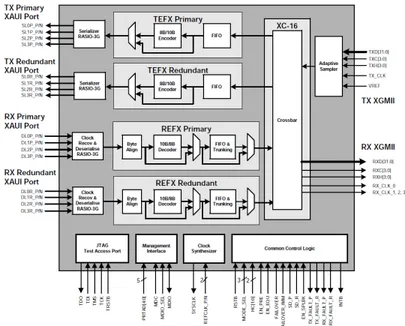
Figure 2.1: NWP block-diagram, on the green-dotted box are shown the PHY commodity components that manage the physical level of the links such as electrical signals; on the red-dotted box are shown the 6 link managers, together called TNW, that take care of the PHYs configuration and reliable data transfer. On the blue-dotted box is shown the interface to the CPU, called Input/Output Controller (IOC), it manages the PCIe link to the CPU and the DMA engine.
by applications.
From bottom to top of the NWP stack, the first hardware layer is the Physi-cal Layer (PHY) that takes care of the electriPhysi-cal signals and link establishment, it is based on the commodity component PMC-Sierra PM8358, mainly a
XAUI-to-XGMII SERDES 2 device that allows data communication on four PCIe Gen
1 lanes, with a raw aggregate bandwidth of 10 Gbit/s, value estimated as suffi-ciently large for which application type (mainly LQCD) NWP has been developed for[25][26]. The choice for a commodity device allows to move outside the FPGA the most timing-critical logics, also the use of a well-tested and cheap transceiver based on commercial standard shorten the development time.
The second HW layer, called Torus Network (TNW) is one of the two layers implemented on the FPGA, a “Xilinx Virtex-5 lx110t” for the QPACE machine or an “Altera Stratix IV 230 GX” for AuroraScience, TNW has been written in VHDL language, mainly his purpose is to implement a custom communication protocol optimized for low latencies. This layer exports the injection and recep-tion buffers to exchange data between nodes, as well as the rules to obtain a re-liable link among an unrere-liable electrical path. TNW task is also to act as the Medium Access Control (MAC) for the PM8358 so it implements the modules to configure and check the PHY.
The third and last layer of the hardware stack. is the “Input/Output Controller” (IOC) and will be explained in detail in chapter 3.2. The purpose of the IOC is to export to the CPU the injection, reception and control/status interfaces, providing a translation layer between the CPU’s Input/Output system and the TNW.
The software layers, are explained in detail in chapter 4. They are tailored to provide a convenient an efficient access to the NWP from thread-applications. For this purpose I developed a driver for the Linux operating system and a Low Level Library (LIB), allowing threads to directly access the injection buffers avoiding time overhead from frequent context switches between user- and kernel-mode.
The NWP provides the hardware control of the data transmission and has in-jectionand reception buffers for each of the six links, the applications access the torus-network by (i) moving data into the injection buffer of the NWP of sending node, and (ii) enabling data to be moved out of the reception buffer of the NWP of the receiving node. Thus, the data transfer between two nodes proceeds according
2XAUI means “10 GigaBit Attachment Unit Interface” while XGMII means “10 GigaBit
Me-dia Independent Interface” (compliant to IEEE 802.3ae standard). SERDES means serializer/de-serializer, deriving from the conversion from parallel data at one side of the device to serial data at the other side and vice-versa.
to the two-sided communication model3, where explicit operation of both sender
and receiver are required to control the data transmission [29].
Data is split in a hierarchical way into smaller units during the various trans-mission steps. The size and name of these units depends on the step which is considered. Applications running on CPUs exchange “Messages” with a variable size between a minimum of 128 Bytes and a maximum of 256 KBytes, but always in multiples of 128 Bytes. At the NWP level a message is split into “Packets” with a fixed size of 128 Bytes. They are the basic entity which the network processors exchange. Inside the NWP a packet is split into “Items”, which have a size of 4 or 16 Bytes, depending on the stage of the NWP considered.
Tracing a CPU-to-CPU data transfer over the 3d-torus the following steps oc-cur:
1. The application calls the send operation specifying over which of the six links to send the message. It simply copies the message-items from the user-buffer to the address-space where the injection buffer of the link is mapped. Depending on the architecture and the I/O interface of the CPU, this operation can be imple-mented according to different schemes.
2. As soon as an injection buffer holds data, the NWP breaks it into fixed-size packets and transfers them in a strictly ordered and reliable way over the corre-sponding link. Of course, the transfer is stalled when the reception buffer of the destination runs out of space (back-pressure).
3. The receive operation on the destination CPU is initiated by passing a credit to the NWP. The credit provides all necessary informations to move the received data to the physical-memory and to notify the CPU when the whole message has been delivered.
To allow a tight interconnection of processors with a multi-core architecture, the TNW also supports the concept of virtual channels to multiplex multiple data streams over the same physical link. A virtual channel is identified by an index (or tag) which is transfered over the link together with each data packet. This is needed to support independent message streams between different pairs of sender and receiver threads (or cores) over the same link. The virtual channels can also be used as a tag to distinguish independent messages between the same pair of sender and receiver threads[29].
In the rest of this chapter I explain the PHY and TNW hardware layers in detail.
2.1
Two-Sided Communication Protocol
The “Two-Sided Communication Protocol” is based on the classic approach to distributed memory parallel systems programming, the “message passing” model where messages are exchanged using matching pairs of send and receive function calls from the threads involved into the communication. The basics of this model are widely used in Message Passing Interface (MPI) programming and the most important concept is the notion of matching. Matching means that a receivecall does not deliver just the next message available from the transport layer, but a message that matches certain criteria. Typical criteria implemented are sender ID, size or the user specified tag.
The NWP implementation of the Two-Sided Communication Protocol is based on three separated operations, one to send data and two to receive them;
the first operation, called SEND, allows to move messages from the user-space of the sending thread directly into the injection buffers of the network processor, triggering the message delivery to the peer-entity at the other side of the commu-nication link.
The remaining two operations are both required to receive data, the first operation is called CREDIT, the receiving thread must issue it to NWP as soon as possible to provide the basic information to deliver the incoming messages directly to the main memory of the receiving node, once the CREDIT has been issued, NWP can autonomously end-up the message delivery and the thread can spend to any other operation that does not require the incoming data. The second operation to receive a message is POLL, this operation is undertaken by the thread when it requires the incoming data to go on with computation, calling POLL is tested the condition of completely delivered message, once the condition is true the thread can proceed using data, otherwise it keeps waiting.
The whole mechanism is based upon the use of tags, each SEND has its own tag that must match with the corresponding CREDIT/POLL tag on the receiver side, subsequent messages with the same tag must be sent in the same order as the CREDIT/POLL are issued to avoid data loss or corruption.
The above mechanism limits the need of temporary buffers to store incoming data and any other complex infrastructure at operating system level to keep care of transactions, leaving the whole communication in user-space under the control of the application.
Figure 2.2: Node-to-node reliable communication diagram, it is based on a ACK/NAK protocol. Each packet is protected by a CRC and a copy of data is stored into the Re-send Buffer (RSND), if the CRCs on TX and RX match the packet is accepted issuing an ACK or otherwise it is discarded issuing a NAK. The ACK feedback removes the packet from RSND while a NAK implies the resend of the packet.
2.2
TNW Communication Protocol
The entities at the end-points of the Physical Link Layer are the transmitter (TX) and the receiver (RX), the communication among them follows few simple rules, a “Packet-Based ACK/NAK Protocol[2]”, that allow a reliable data exchange. This protocol implements only the detection of possible errors, not their correction, if an error occurs data are simply re-transmitted. The basics of the above men-tioned protocol require a data unit called “packet”, with a well-defined format and size, that are received by RX in the strict order they are sent by TX, even despite an error occurred; the entire packet is protected by a Cyclic Redundancy Check (CRC) calculated upon the entire packet and appended to it on transmis-sion, a copy of the packet is stored into a Re-send Buffer (RSND) in the case it must be re-transmitted, on the receiver side the CRC is re-calculated and compared with the appended one, if they match an Acknowledge (ACK) is sent-back by the FEED module and the packet is accepted by RX and stored into the Receiver Buffer (RCV) while dropped by the resend-buffer, on the other hand the packet is dropped by RX and a Not Acknowledge (NAK) feedback is sent-back, at this point TX enters in RESEND mode and re-send the copy stored into the resend-buffer until it is not acknowledged by RX or until a time-out occurs. The above mechanism is shown in figure 2.2.
Acknowledging one packet per time before sending next could be a waste of bandwidth, a way to maximize throughput is to send a continuous packet-flow while waiting for feedbacks, this implies that each packet has his-own sequence number that must be claimed into feedback and the calibration of resend-buffer to
store a sufficient number of packets corresponding to in-flight packets. When an error occurs, RX drops the faulted packet and sends-back a NAK with the corre-sponding sequence number, discarding all the in-flight packets that follow without issuing feedbacks, TX stops sending new packets and issues a “RESTART” com-mand to RX followed by the packets with equal and greater sequence number then the one on the feedback, after RX receives the RESTART it behaves as usual. “receiver-buffer’ Protocol rules:
• packet format and size are well-defined
• packet is entirely protected by a CRC and has a sequence number
• RX must receive packets in the same order TX send them, also despite any error occurrence
• TX computes the CRC and appends it to packet
• RX re-computes CRC, if it matches with appended one, send-back an Acknowledge (ACK), if not, send-back a NAK (not acknowledge)
• packet is stored into a resend-buffer until not ACK by RX • resend-buffer must fit in-flight packets number
Required control characters:
• ACK to acknowledge a packet that match with his-own CRC
• NAK to not acknowledge a packet that does not match with his-own CRC • RESTART to stop RX to discard incoming packets after an error occurs The “TNW Communication Protocol” also manages the case the receiver-buffer runs-out of space, as explained in section 2.1, the CPU must to issue a CREDIT to RX as soon as possible, ideally before the first packet of a message has been transmitted by TX, in this case data can stream directly from the link to the main memory without lying too much time into RCV. To the contrary, if TX starts to transmit the message before the CREDIT has been issued, RCV can quickly run-out of space, and all the further incoming packets are treated by RX as faulted, discarding them and sending-back to TX a NAK feedback; at this point TX will behaves as usual, entering in RESEND mode until the packets are not acknowledged by RX or a timeout occurs. If a CREDIT is issued to RX before the timeout occurrence, the communication restarts.
Figure 2.3: Block-diagram of the commodity PHY PMC-Sierra PM8358. On the left-side are visible the Primary/Redundant serial ports (XAUI) used for the node-to-node communications; on the right-side are visible the parallel ports (XGMII) managed by the TNW module.
2.3
Physical Link Layer
The Physical Layer (PHY) is the unreliable data path between the network proces-sors. The bandwidth required for the project described in this thesis is 10 Gbit/s. This can be reached, for instance, by using a “PCI Express Generation 1” link with 4 lanes (4x). The link is implemented by using the commodity PHY component “PM8358” manufactured by PMC-Sierra.
The PM8358 is a multi-protocol silicon device for telecommunication and has the block-diagram as shown in figure 2.3. This PHY implements several telecom standards, such as PCIe, Gigabit Ethernet, 10 Gigabit Ethernet, Infiniband, Com-mon Public Radio Interface, High-Definition TV, etc. and supports a wide range of operative frequencies (1.2 to 3.2 GHz).
The PM8358 is mainly a XAUI-to-XGMII serialization/deserialization device (SERDES). While XGMII allows only a limited signal routing (maximum 7 cm)
4, the XAUI ports provide serialized data over LVDS pairs. These allow to drive
drive signals over a longer distance, for instance over a back-plane or cable for node-to-node communication.
The XGMII ports are parallel buses connected to the application logic im-plemented inside the FPGA. Each port has a 32-bits data-path (TXD and RXD) and 4 bits for flow-control (TXC and RXC). These lines operate in Double Data-Rate (DDR) mode with two independent clocks (TXCLK and RXCLK). Each 8 bits of the data-path have one associated bit of flow-control, which flags whether the data is a “data character” or a “control character”. The latter are functional to the correctness of the transmission and management of the link.
Data serialization includes the “8b/10b Encoding” encoding stage to reduce ElectroMagnetic Interference (EMI) noise generation in different manners and to reduce data corruption. The 8b/10b Encoding embeds the clock of the data source into a data-stream. This eliminates the need of a separate clock-lane which would generate significant EMI noise and it also keeps the number of ‘1’ and ‘0’ trans-mitted over the signal lines approximately equal to maintain the DC component balanced and to avoid interference between bits send over the link, see [2] for more details.
The configuration/status of the PHY is accessible via MDIO 5 (Management
Data Input/Output). This it is a serial master/slave protocol to read and write the configuration registers on a device. In our case the logical master is the NWP (physically one the FPGA) and the slave is the PHY. The master can access dif-ferent slaves via a two-signal bus shared by them. One signal is the “Management Data Input/Output/Serial Data Line” (MDIO) that actually carries control and sta-tus informations. The other is the “Management Data Clock” (Management Data Clock (MDC)), which is just a strobe, i.e. the MDIO line is sampled at the rising edge of MDC.
The NWP interconnects the nodes of a machine as edges of a three-dimensional grid with toroidal re-closing. Multiple grids with this topology can be connect to-gether simply “opening” the re-closings and pairing them, resulting in an extended single machine with more nodes. Vice versa, a single machine can be partitioned into multiple independent ones just by “cutting” some connections and re-closing them into the new smaller partition. This allows to assemble a machine with an arbitrary number of Nx× Ny × Nz nodes that can be partitioned as independent
machines or expanded as needed.
for more details.
5For the specific, the MDIO “Clause 45” defined by IEEE 802.3ae that allow to access up to
Figure 2.4: Re-partitioning example of a four-nodes machine. Depending on configu-ration of PHY ports, primary (blue lines) or redundant (red lines), the machine can be configured as one four-nodes machine (layer “B”) either as two separated two-nodes machines (layer “C”) without re-cabling the connections.
Usually such a re-partitioning of a machine would require re-cabling. How-ever, exploit the fact that the PM8358 provides a “Primary” and a “Redundant” XAUI port. They are both connected to XGMII interface via an internal crossbar and are mutually exclusive. This feature allows to physically connect one PHY with two others instead of one. Thus, by selecting at configuration time which of the two physical links will be actually activated, we can re-partition the machine without the need for re-cabling.
An example of re-partitioning is shown in figure 2.4. The layer “A” of the figure shows a four-nodes machine, where each node is connected to its nearest neighbors only along one dimension, the dotted-blue lines are the connections between primary ports of the PHYs while the dotted-red lines are the connec-tions between redundant ports (nothing prevents to connect a primary port to a redundant). The machine can be configured as one four-nodes machine enabling via software all the connections on primary ports (blue lines) and disabling the connections on redundant (red lines), as shown in layer “B”. Alternatively the machine can be configured as two separated two-nodes machines, enabling the redundant links among nodes 0 and 1 and among nodes 2 and 3, preserving the primary connections among node-pairs, as shown in layer “C” of the figure.
2.4
Torus Network Layer
The basic idea underlying TNW is to provide a high-bandwidth low-latency point-to-point link among two computing-nodes on a massive parallel machine for sci-entific computing.
NWP is based on the 3D-torus topology so it must manage six links, one per spatial direction, all those links lie on the Torus Network (TNW) hardware layer and each of them is the Medium Access Control (MAC) for the Physical Layer (PHY) of the link connecting two computing-nodes, implementing a reli-able communication among a non-relireli-able media. To allow a tight interconnec-tion of processors with multi-core architecture, TNW must support an abstracinterconnec-tion mechanism to virtually provide a dedicated link among a pair of cores belonging to different computing-nodes, I used the “Virtual Channels” mechanism to mul-tiplex data streams belonging to different core-pairs over the same physical link. TNW implements a “Two-sided Communication Protocol” where data exchange is completed with explicit actions of both sender and receiver, see section 2.1 for a more detailed explanation of the Two-sided Communication approach.
Each TNW link is mainly divided into “transmitter” (TXLINK) and “receiver” (RXLINK) sub-systems that will be presented in detail in sections 2.4.1 and 2.4.4, each link also implements a Test-Bench (TB) module, explained in section 2.4.5, fully controlled via register interface, that features a data generation/check mech-anism to fully test the low-level activities of TNW. On the receiver-side I also implemented a synchronizer (Receiver Synchronizer (RXSYNC)), explained in section 2.4.3, to efficiently synchronize data among the clock-domain of the PHY (125 MHz DDR) and the clock-domain of TNW (250 MHz Single Data-Rate (SDR))6. In figure 2.5 is shown the diagram of the TNW layer.
2.4.1
The “TXLINK” Module
The Link Transmitter (TXLINK) has the purpose to send the data injected by the CPU over the physical link in a reliable manner, it also takes care to manage and configure the physical link driver (PHY) via the MDIO interface.
The main components of TXLINK are the “Injection Buffer” called TXFIFO,
6The PHY outputs data @125 MHz in Double Data-Rate (DDR) mode, considering two
sub-sequent data, one is produced on the rising-edge of the clock while the other is produced on the falling-edge. The TNW clock-domain is 250 MHz and accepts input data in Single Data-Rate (SDR) mode, in this case input data are expected on the rising-edge of the clock.
Figure 2.5: Block-diagram of the TNW layer. The bottom-side shows the transmitter path, data flows from the CPU interface (IOC) to the physical-link (PHY), the transmission is managed by the TXLINK module. The top-side shows the receiver path, data flows from the physical-link (PHY) to the CPU interface (IOC), the RXSYNC module synchronizes the incoming data between the PHY clock-domain and the TNW clock-domain; the RXLINK module manages data reception. The TB module features a data generation/check mech-anism to fully test the TNW low-level activities, it’s interposed between the CPU interface and the TNW’s injection/reception buffers, when not enabled it is completely transparent to the other modules and acts like a pass through without affecting data-flow. Otherwise it separates TNW from the CPU interface, autonomously managing the data-stream.
Figure 2.6: Diagram of the TXLINK module. The upper section is the data transmission pipeline, it includes the injection buffer (TXFIFO) and the modules to implement the cus-tom packet-based ACK/NAK protocol, RSND stores packet-copies in case they must to be resent due to corruption among the link, CRC module computes the protection-code to validate or not the packet at the receiver-side. The lower section is the register access including the MDIO interface to the PHY.
the “Re-send Buffer” called RSND, the “CRC7module” and the Transmission
Fi-nite State Machine (TXFSM). A diagram of TXLINK is shown in figure 2.6. Before describing the TXLINK functionalities, it is important to specify the informations contained into the basic entity managed by NWP: the “packet” that is composed by a header and a 128-bytes payload; the header contains all the informations to fully route data from sender to receiver, these informations are: the Link-ID (LID) that specifies over which one of the 6 links data will be sent, the Virtual Channel ID (VCID) that specifies which virtual channel within the same link will be used, the Remote-Address Offset (RAO) that specifies the offset to write data respect to the memory-address of the reception buffer at the receiver side of the link. The payload contains the actual data to be sent.
A hardware module, located into the IOC module so external to TNW, uses the LID field of the packet-header to select in which of the 6 TXFIFOs to inject data, preserving VCID and RAO fields, the TXFSM is sensitive to the injection
7The CRC module directly derives from the VHDL code provided in the paper "Parallel CRC
Realization[30]" by Giuseppe Campobello, Giuseppe Patané, Marco Russo. This module imple-ments a parallel method to calculate CRC checksums, allowing it’s use in high-speed communica-tion links.
buffer status, when at least one packet is stored there, TXFSM starts to extract it and route it through the transmission pipeline. During the 4-stages transmission pipeline a new header is assembled using VCID and RAO fields and the pay-load is appended. The paypay-load is stored inside the TXFIFO in 8 16-bytes items while during the pipeline it is extracted as 32 4-bytes items due to the PHY data-interface width. While the packet steps into the pipeline a copy is stored into the re-send buffer where it lies ready to be retransmitted in case the receiver claims a corrupted reception; the copy is removed only if the receiver claims a correct re-ception of the packet. The above scheme is based on a ACK/NAK protocol where the sender trails to the packet a 4-bytes CRC item calculated over the whole packet and the receiver recalculates the CRC comparing it with the trailed one, if CRCs match, the packet is accepted and a positive feedback (ACK) is sent back, other-wise the packet is discarded and is sent back a negative feedback (NAK). A more accurate description of the protocol used for a reliable communication in TNW is exposed into section 2.2. A remarkable thing to keep in mind is that a TNW link is composed by one TXLINK and one RXLINK modules, the TXLINK module of an end-point is directly connected with the RXLINK of the other end-point, so RXLINK checks the correctness of sent data but only TXLINK can send feed-backs to the peer, at this purpose TXLINK accepts requests from RXLINK to send back feedbacks to the peer; the feedback sending has a highest priority respect to data.
TXLINK contains a set of configuration and status registers to control the configuration of the link and to provide a snapshot of its status.
2.4.2
The MDIO Interface
TXLINK manages the configuration of the PHY device via the MDIO interface, briefly described in section 2.3. The MDIO module is based on a FSM that man-ages read/write operations to the PHY that are always composed by an ADDRESS frame followed by a READ or WRITE frame, the frame layout is shown in figure 2.7 and follows the explanation, the PREAMBLE, a sequence of 32 “logic 1s”, is at the beginning of each frame to establish synchronization among endpoints; ST is the “Start of frame”, a pattern of 2 “logic 0s”;
OP is the “Operation code”, 0b00 for ADDRESS frame, 0b11 for READ frame,
0b01for WRITE frame;
PRTAD is the “Port address” and identifies the PHY to which the operation has been issued;
Figure 2.7: MDIO frames diagram
MDIO frames diagram.
in this case it is set to DTE-XS (Dumb Terminal Emulator) 0b00101;
TA is the “Turn-around”, a 2-bit time spacing between DEVAD and DATA/AD-DRESS fields to avoid contention during a read transaction, during a read trans-action, both the master and the slave remain in a high-impedance state for the first bit time of the turnaround, and the slave drives a “logic 0” during the second bit time of the turnaround, during a write transaction, the master drives a “logic 1” for the first bit time of the turnaround and a 0 bit for the second bit time of the turnaround;
DATA/ADDRESS is a 16-bit field that, depending on the frame, contains the reg-ister address to operate to or the read/write data.
I implemented the MDIO module to be accessible via internal register of TXLINK, a write operation addressed to the MDIO_W register triggers the MDIO module for a write transaction to the PHY, the MDIO_W register layout includes the address of the PHY register where to write to and the data to be written, a busy-flag in MDIO_W reflect the status of the MDIO transaction. Same concept is applied to the MDIO_R register, a write operation addressed to this register triggers the MDIO module for a read transaction from the PHY, the MDIO_R register layout includes the address of the PHY register to read and a busy-flag reflect the status of the MDIO transaction, when the transaction is done, the data field of MDIO_R contains the value read from PHY.
2.4.3
The Receiver Synchronizer
The RXLINK module, as whole the TNW layer, works on a 250 MHz clock-domain where data are sampled in Single Data-Rate (SDR) mode, considering two subsequent data both are sampled on the rising-edge of the clock, as shown on the left-side of figure 2.8, while the PHY outputs data @125 MHz in Double Data-Rate (DDR) mode, considering two subsequent data, former is produced on the rising-edge of the clock while the latter is produced on the falling-edge, as shown on the right-side of figure 2.8, these data are in sync with the clock recovered from the 8b/10b data-stream received.
Figure 2.8: Differences among “Single Data Rate” (SDR) mode and Double Data-Rate (DDR) mode. In SDR data are sampled either on rising or falling edge of the clock, in this example data are sampled on rising edge. In DDR data are sampled on both clock edges.
Figure 2.9: RXSYNC diagram, data are synchronized among PHY’s and TNW’s domains using a FIFO. To avoid FIFO-full due to the differences among clock-frequencies, not all the incoming data are pushed-in, the control-character not needed by the TNW protocol are removed by the IDL_RM logic. The READ logic extracts data as soon as they are available.
To deal with the above mentioned characteristics, is required a synchroniza-tion layer between PHY and TNW clock-domains that allows to get in sync data in a reliable manner. At this purpose I implemented the Receiver Synchronizer (RXSYNC) module, shown in figure 2.9.
The data clock-domain transition is implemented using a “Synchronization FIFO” (SYNC_FIFO), data are written in sync with PHY’s clock and read in sync with TNW’s clock. First of all the 125 MHz output from the PHY is doubled to 250 MHz using a Phase Locked Loop (PLL), in this way data can be sampled in SDR mode instead of DDR.
The custom protocol used for TNW-to-TNW communications foreseen the injec-tion of IDLE code (K28.3) every 256 consecutive-packets sent to allow for suffi-cient clock rate compensation between the end-points of a link; these IDLEs are required just on the earliest stage of the receiver so they are removed from the data stream by the “Idle Removal” (IDL_RM) logic and not written into SYNC_FIFO to avoid FIFO full. To the contrary data-packets are stored into the FIFO and can
proceed to the TNW clock-domain.
The empty signal of the FIFO triggers the READ logic to extract data that are then output.
2.4.4
The “RXLINK” Module
The purpose of the Link Receiver (RXLINK) is to receive packets from his peer entity in a reliable manner and deliver data to the CPU.
The basic idea underlying the structure of RXLINK is to implement the two-sided protocol and to provide a set of Virtual Channel (VC) to allow communi-cations of independent thread-pairs running on adjacent computing-nodes shar-ing the same physical link or to allow different message priorities. Each VC is managed with a credit-based mechanism where the CPU provides to TNW the informations to complete the message delivery, the “credit” precisely, these infor-mations contains the IDs of both link and VC (LID and VCID) the message will come, the main memory-address (CRDADDR) to deliver data and the message size (SIZE), the last information is the Notify-ID (NID), this is the offset respect to a particular main memory-address (Notify Base Address Register (NTFBAR)) where the CPU will wait the notification from TNW that the whole message has been received and CPU can use data. The messages-items, called packets, in-coming from the link are stored into TNW buffers until the CPU does not issues the corresponding credit, these buffers can rapidly run out of space and to cause the stall of the communications, this requires that for each send operation must be issued the corresponding credit, and referred to the same link and VC, they must be issued in strictly order; to avoid that the stall of a VC affects the others, each virtual-channel has his own credit-based mechanism explained later in this section.
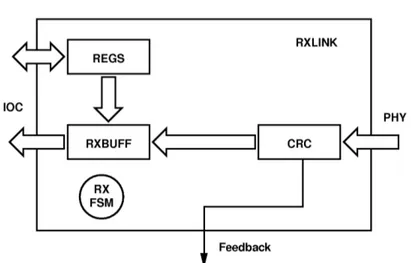
RXLINK is mainly composed by the Reception Finite State Machine (RXFSM), the “CRC” module and the “Reception Buffer”(RXBUFF) as shown in figure 2.10. RXFSM takes in charge to supervise the reception of the packet-items from the PHY and to verify their correctness with the help of the CRC module, for each incoming packet is recalculated the CRC and, if it matches with the trailed one, data are stored into RXBUFF and is triggered TXLINK to send to the peer entity a positive feedback (ACK), otherwise is triggered a negative feedback (NAK), each feedback is accompanied by the sequence-number relative to the packet. The de-tailed description of reliable communication protocol is in section 2.2.
RXBUFF is the most complex module of the receiver block, it actually imple-ments the logic to manage the two-sided communication protocol and the
virtual-Figure 2.10: Diagram of the RXLINK module. The lower section includes pipeline where data are checked using the CRC method and the reception buffer (RXBUFF) to store data before sending them to the CPU. The upper section is the register access.
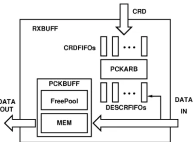
channels. A diagram of RXBUFF is shown in figure 2.11.
Each Virtual Channel (VC) has his own private Credit FIFO (CRDFIFO) and Descriptor FIFO (DESCRFIFO), the former stores the credits issued by the appli-cation while the latter stores the descriptors (actually the headers) of the received packets, when a packet has been received and validated, the payload is stored into the Packet Buffer (PCKBUFFER) while the header is stored into the DESCR-FIFO relative to the VC the packet belong, if the Packet Arbiter (PCKARB) finds a match between a DESCR and a CRD for the corresponding VC, it triggers the operations to deliver data to the CPU. When a credit is exhausted, in other words all the packets relative to the same message are delivered to CPU, a particular transaction called “notify” is sent to the CPU, telling that the whole message has been arrived and data are ready to be used by the CPU.
The PCKBUFFER is designed around a single memory block, common to all virtual channels, an internal module called “free-pool” keeps trace of the unused memory-locations, so each incoming packet can be stored into an arbitrary loca-tion, independently from the VC it belongs and packets belonging to the same message could be stored into non-adjacent memory-locations, this allows to effi-ciently manage the TNW storage without reserving a fixed amount of memory to each virtual-channel that could results in a waste of memory-space.
The main memory-addresses where to send data and notifies are a combination of base-addresses stored into internal registers and some fields of both credit and
Figure 2.11: Detailed view of RXBUFF, credits provided by CPU are stored into the related CRDFIFO based on the virtual-channel they has been issued for, the incoming data are stored into MEM while the header (descriptor) is stored into the related DESCR-FIFO depending on the virtual-channel they belong, if the Packet Arbiter (PCKARB) find a match between one descriptor and one credit, the interface with the CPU is triggered to move data into main memory.
descriptor. For data there is one Credit Base Address Register (CRDBAR) register per virtual-channel, it stores the main memory-address where starts the address-space of the buffer to deliver data relative to the specific VC, at this address is summed the Remote-Address Offset (RAO) field stored into the descriptor of the packet. Same concept is used to retrieve the physical memory-address to notify the CPU that a message has been completely delivered, a register called Notify Base Address Register (NTFBAR) stores the memory-address where starts the address-space of the buffer to deliver the notification relative to the specific message, at this address is summed the Notify-ID (NID) field stored into the credit for the message, it specifies the offset to write the notify respect to NTFBAR.
2.4.5
The “Test-Bench” Module
The Test-Bench (TB) features a data generation/check mechanism to fully test the functionalities of TNW such as the register access and the communications. It’s interposed between the CPU interface and the TNW’s injection/reception buffers, when not enabled it is completely transparent to the other modules and acts like a pass through without affecting data-flow. Otherwise it separates TNW from the CPU interface and manages autonomously the data-stream. TB is mainly com-posed by a data generator Data Generator (DATAGEN) and a Data Checker (DAT-ACHK), as shown in figure 2.12,
both can manage a sequential counter or a pseudo-random sequence of data, the former has been used in the earliest phases of the link development where the data transmission has been controlled using a simulation tool and it was more simple to follow sequential data on the simulation window, the latter has been used for all the actual link tests. DATAGEN is controlled by a finite-state machine (FSM) managed via configuration registers and sensitive to the status of the in-jection fifo of the link to generate data on-the-fly and to inject them only when the fifo is not full, two 64-bits pseudo-random generators has been implemented to fit the 128-bits data-bus of the injection buffer, each generator implements the following equation to generate data,
rnd = rndprev⊕ (C + swap(rndprev))
where the swap() function permutes the 17 lowest bits of ndprevwith the 47
high-est bits. The sequential number generator is a 32-bits counter replicated 4 times to fit the 128-bit data-bus. DATACHK is similar to DATAGEN it is managed by configuration registers and is controlled by a FSM, it implements both the same
Figure 2.12: Block-diagram of the TB module. It’s interposed between the CPU interface and the TNW’s injection/reception buffers, when not enabled, the switches act like a pass through between IOC and TNW, so TB is completely transparent to the other modules, otherwise TB separates TNW from the CPU interface and manages autonomously the data-stream. All the TB’s functionalities are fully controlled by register interface.
sequential- and the pseudo-random number generators, here the incoming data are compared to the internal-generated ones and if they differ an error-counter is incremented.
A set of internal registers manage and keep track of the test bench activities, such as the control of DATAGEN and DATACHK, e.g. selecting which kind of data to generate (random or counter), as well to introduce voluntary errors in-side the data-flow, keep track of the whole amount of data generated/checked and eventually the number of errors detected.
Chapter 3
Network Processor’s CPU Interface
In this chapter I explain the general mechanisms for moving data between the main memory of the CPU and the I/O devices. I then discuss the best way to map the transactions between CPU and I/O devices on the specific PCI Express Protocol and describe the design and implementation of the VHDL modules to interface the network processor with the CPU.
3.1
Transaction Models
Data exchange between CPU and Network Processor (NWP) can be implemented in several ways, here follows the descriptions of four of these methods applied to the Intel Architecture, analyzing pros and cons.
To send a message along a TNW link, from the main memory point of view, requires to move data to the injection buffer of the link. In NWP jargon, data movement can be done in two ways, the former, called Processor PUT (PPUT), is shown in the left-side of figure 3.1, it foreseen that the CPU actively loads data from main memory (1) and stores them into the injection buffer (2), one-by-one, being involved for the whole time the data movement requires. Beside is shown the temporal diagram of the data movement between CPU and NWP using the PPUT method. The latter method, called Network GET (NGET), is shown in the right-side of figure 3.1, here the CPU simply gathers informations about the data movement (address and size) and pass them to the network processor (1) that will autonomously retrieve data from main memory (2,3) without any other CPU intervention; CPU will be notified about the completion of the data movement (4). The temporal diagram of NGET method is shown beside.
Figure 3.1: Diagram of PPUT and NGET transaction-methods to send data over the link, targeting the Intel Architecture. With PPUT the CPU directly loads data from memory (MEM) to its internal registers (1), then it stores data (2) to the injection buffer (TX) of the Network Processor (NWP); the CPU is involved to data movement instead of computation for all the transaction-time. With NGET the CPU collects informations about transactions and pass them to the NWP (1) that will independently interact with memory to retrieve data (2,3), at the end of the transaction NWP notifies CPU (4); in NGET computation and data movement can be overlapped but it suffers of higher latency respect to PPUT due to the higher number of CPU-NWP interactions. Beside of each transaction-method is shown the relative temporal diagram of the operations.
As predictable, in Intel Architecture, the PPUT method offers lower latencies respect to NGET due to the lesser number of interactions required; the PPUT drawback is that it keeps the CPU involved until the end of transaction, preventing it to perform calculations, on the contrary NGET allows the CPU to do not care about the data movement, letting it available for calculations.
On the receiving side, to receive a message from a TNW link requires to move data from the receiver buffer of the link to main memory, and also in this case there are two ways to do it, the former, shown in the left-side of figure 3.2, is called Network PUT (NPUT), in this case, the CPU provides to the network processor the informations about the message it is waiting for (1), such as the address to deliver it and its size, calling these “credit” (CRD); as well as message’s fragments have been received the network processor independently interact with the memory controller to move data to main memory (2) at the address provided by the CPU; then the CPU has to be notified (3) about the whole message reception. Beside is shown the temporal diagram of the data movement between NWP and CPU using the NPUT method. The latter method, shown in the right-side of figure 3.2, is called Processor GET (PGET), here the CPU is actively involved to the receive operations; when the network processor has been received a defined amount of data, it notifies the CPU (1) that will issue read operations (2/3) to the network device to retrieve data from the receiving buffer and then move them into memory. The temporal diagram of PGET method is shown beside.
In NPUT method, once the CPU has issued the credit, it can continue with other tasks, leaving to the network processor the interaction with memory to carry-out the data-reception, in this way computation and communication can be over-lapped; in PGET the CPU must to issue read operations to retrieve data from NWP, limiting the overlap of computation and communication.
The Network Processor object of this thesis interfaces with the CPU via the PCI Express bus. In this section I describe how to map the transaction methods described in section 3.1 to the operations implemented by the PCI Express Proto-col.
The PCI Protocol, from whom PCIe derives, provides three transaction modes[2] on which can to map PPUT, NGET and NPUT transaction models; to understand the differences among them I will explain the transactions considering the sim-plified architecture in figure 3.3, here two devices (device0 and device1) are at-tached to the PCI bus, the CPU can access the PCI via a companion-chip called “ChipSet”, it also integrates the memory-controller to access the main memory modules.
Figure 3.2: Diagram of NPUT and PGET transaction-methods to receive data from the link. With NPUT the CPU provides a credit (1) to the Network Processor (NWP), incom-ing data are written to memory (2) accordincom-ing with the credit-information, when the whole message has been received the CPU is notified (3). With PGET the NWP notifies (1) the CPU that some data has been arrived, the CPU issues read operations to retrieve data from RX-buffer (2/3) and moves them into memory (4). Beside of each transaction-method is shown the relative temporal diagram of the operations.
The first mode is Programmed Input/Output (PIO), it can be directly mapped to the PPUT model, when the CPU wants to start a write transaction to a target de-vice, it must load data from memory into its internal registers and then store them to the target device address-space, in a read transaction the CPU must interrogate the target device and then waiting for the response. The PIO mode involves both the CPU and the target device until the transaction is carried out, keeping busy the CPU on data transferring instead of computation, to transfer small amount of data from memory to the target device this is not an issue, actually has better per-formance in terms of latency, to the contrary, for large data transfer the PIO mode subtract computational resources.
The second mode is Direct Memory Access (DMA), from the network proces-sor point of view it can be directly mapped to NGET respect to data-read opera-tions and mapped to PPUT respect to write operaopera-tions. In DMA a PCI device can directly access the main memory both for load and store operations, without the intermediate step of the CPU registers, letting the CPU to continue computing; considering a data transfer from memory to a target device as done previously for PIO mode, the CPU must to gather the informations to carry-out the transaction and pass them to the device, at this point the CPU job is done and can continue
Figure 3.3: PCI transaction modes, in PIO mode both CPU and target device are involved until the end of the transaction, data are transferred from the internal registers of the CPU to the address-space of the target device. In DMA the device directly access the memory without CPU intervention, just interacting with the memory controller, letting the CPU freely computing. In Peer-to-peer mode a master device can autonomously access a target device.
the computation, the device can autonomously interact with the memory to trans-fer data. DMA mode suftrans-fers of higher latency compared to PIO due to the initial transaction between CPU and device to start the data transfer but this mode allows to free the CPU from any other intervention, letting it to dedicate to computing instead of data transfer.
The third mode is Peer-to-peer, it is not implemented by NWP, and it provides the direct data transfer between two PCI devices, for store operation a master di-rectly move data to the address-space of the target, while for load operation the master interrogates the target device and then waits for the response.
The PCIe Protocols foreseen 4 transaction types, depending on the address-space they are generated. The 4 address-address-spaces are I) Memory, to transfer data to or from a location in the system memory map; II) IO, to transfer data to or from a location in the system IO map, this address space is kept to compatibility with legacy devices and is not permitted for Native PCI Express devices; III) Configuration, to transfer data to or from a location in the configuration space of PCIe devices, it is used to discover device capabilities, program plug-and-play features and check status; IV) Message, provides in-band messaging and event-reporting without consuming memory or IO address resources.
Of all the above mentioned transaction type, in the NWP design I used only the “Memory Address-Space”, it supports both Read and Write transactions called “Memory Read Request” (MRd) and “Memory Write Request” (MWr). Each of the above mentioned operation is mapped into the data transfer unit of the PCIe protocol, the Transaction Layer Packet (TLP). Memory transaction TLP has a well-know format and size, it is composed by a header and a payload (here I do not consider the optional digest), the header includes lots of informations where the most relevant for NWP are shown in figure 3.4, they are the type of transaction, given by the union of “Type” and “Format” fields; the “Traffic class” to provide differentiated services for different packets; the “Attributes”, the “Requester ID” that identifies the device initiates the transaction; the “Tag” that identifies each outstanding request issued by a requester; allowing a device to issue more trans-actions at the same time; the memory-address for which the transaction has been issued; and last the payload size (if any).
Figure 3.4: PCI Express (PCIe) memory request headers, top-side shows the 4DW header used to operate on a 64-bit address-space, bottom-side shows the 3DW header used to operate on a 32-bit address-space
The Memory Read Request (MRd) must be completed returning-back to the requester a Completion with Data (CplD), where the payload contains the read value while the header requires some fields coming from the request, such as the “Traffic Class”, the “Attributes”, the “Requester ID”, the “Tag” to match the outstanding request with the completion, the “Byte Count” that specifies the re-maining bytes count until a read request is satisfied, and the “Lower Address” that are the lowest 7 bits of address for the first byte of data returned with a read.
Figure 3.5: PCI Express (PCIe) completion header.
Considering the above mentioned memory operations, I can map the PPUT, NGET, NPUT and PGET transaction-methods in PCIe TLPs. PPUT simply trans-lates into a Memory Write Request (MWr) TLP originating from CPU to NWP. NGET is split into four TLPs, the first is a MWr from the CPU to the NWP con-taining all the informations to trigger the DMA transfer from memory to Network Processor, in the specific a MRd from NWP to MEM and a CplD in the oppo-site direction, finally NWP notifies the CPU via a MWr. NPUT requires three
TLPs to carry-out the transaction, the first is a MWr from CPU to NWP to issue the CREDIT, then NWP deliver data to memory and notifies the CPU using two MWr. PGET is mapped to three TLPs, the first is a MWr from NWP to CPU to notify that a message has been received, the CPU then issues one or more MRd to retrieve data from NWP via CplD. A summary of the above operations is shown in table 3.1.
Method Source Dest Operation TLP
PPUT CPU NWP data MWr
NGET CPU NWP snd_req MWr
NWP MEM mem_rd MRd MEM NWP data CplD NWP CPU dma_ntf MWr NPUT CPU NWP crd MWr NWP MEM data MWr NWP CPU ntf MWr PGET NWP CPU ntf MWr CPU NWP rcv_req MRd NWP CPU data CplD
Table 3.1: Mapping of the PPUT, NGET, NPUT and PGET transaction-methods in PCIe TLPs.
3.2
Input/Output Controller
The Input/Output Controller (IOC), is the interface exported to the CPU by the Network Processor (NWP), providing a translation layer between the CPU’s In-put/Output System and the Torus Network (TNW) module; it supports three of the transaction models described in section 3.1, PPUT and NGET for transmission, and NPUT for reception. IOC layer is present only in the AuroraScience ver-sion of NWP, for the QPACE machine I’ve been worked only on PHY and TNW layers.
IOC has been designed to interface with the “Intel Nehalem Processor Family” whom I/O subsystem is managed by the “Tylersburg Chipset” that interfaces with the FPGA, where NWP has been implemented, via PCIe Gen 2 protocol. IOC ac-cesses the PCIe link using two main subsystems, the former manages the