Università degli Studi di Ferrara
DOTTORATO DI RICERCA IN
FISICA
CICLO XXIV
COORDINATORE Prof. Filippo FRONTERA
DEVELOPMENT OF THE INNOVATIVE LEPECVD REACTOR FOR EPITAXIAL GROWTH OF SILICON – GERMANIUM HETEROSTRUCTURES
Settore Scientifico Disciplinare FIS/01
Dottorando Tutore
Dott. GUALDI Federico Prof. GUIDI Vincenzo
_______________________________ ___________________________
(firma) (firma)
3
Abstract
The semiconductor materials both in the form of heteropitaxial and homoepitaxial structures, offer huge potentialities due to a large variety of band energy structures which can be exploited in microelectronics (FET, HBTs) and optoeletronic (lasers, LEDs) devices. However, epitaxial integration of different semiconductors for device development present several issues regarding mainly the minimization of the defects within the heterostructures. To achieve this, materials with similar lattice constant should be used, so that the induced elastic strain in the overgrown film is minimized. Other than the physical constraints however, the choice of the high quality substrate must yield to a cost-effective solution to develop the devices. In the field of microelectronics, the silicon has remained the unparallel material of choice for complementary metal-oxide-semiconductor (CMOS) devices due to its large availability and relative low cost of the raw material. Born in the late 1950s and having since grown into an industry with annual revenues currently in excess of $200 bilion, the modern Si-based semiconductor microelectronics industry is an amazing technical and financial accomplishment. The continuous increase in devices performance requirements have highlighted the main limitation of the silicon device employment. The carrier mobility for both electrons and holes is relatively small respect to the III V alloys, which instead combine high electrical performance with equally high radiation interaction efficiency. Furthermore, the maximum velocity that these carriers can attain under high electric fields is also small, and this limits the cut off frequency of the Si-based microelectronic devices. Due to indirect bandgap also, light emission and absorption is fairly inefficient, making impractical its employment in optoelectronics devices. On the other hand, the higher physical and electrical properties of the III V alloys respect to silicon, are also coupled with relatively high costs. Furthermore, these compounds offer an high application flexibility as the relative composition of these alloys can be also tuned in order to obtain a specific optical or electrical properties.
By employment of the Germanium however, the properties of the silicon can be enhanced drastically. SiGe compounds infact exhibit higher electron and hole mobility even if small relative Ge fraction is added to the silicon. Moreover, the application of strain engineering in microelectronic devices using strain-relaxed SiGe buffer layer have brought a drastic enhancement in electrical properties of silicon. These alloys offers in addition the possibility to integrate the high efficiency III V alloys with low cost silicon substrate. The generally large lattice mismatch between these materials and the silicon, give rise to several issue regarding epitaxy integration. High mismatched heterostructure infact, relax plastically the elastic strain by an uncontrollable process which lead to a high density of induced defects in the grown layers. Several methods have been developed to growth high quality Ge layers
4
onto silicon substrate with only a small dislocation content, such as constant composition thin buffer layers, linearly graded buffer layer and terrace graded buffer layers. On the other hand, in case a pure Ge can be directly integrated into the silicon wafer, a subsequent overgrown of III V alloys can be performed generating a low density of induced dislocations. Also the technique employed for deposition play a determinant role on the final quality of the grown layer. Classical CVD techniques, are able to growth high quality epitaxial layers but suffers generally of a low growth rate. Furthermore, the high thermal budgets required for precursor cracking can lead to several defect generation processes which finally degrade the electrical properties of the grown layer.
In this work, high quality pure Ge virtual substrate (VS) have been grown onto silicon substrate using the low energy plasma enhance chemical vapor deposition (LEPECVD) technique. The innovative epitaxial reactor have been developed at the Physics Department of the University of Ferrara in collaboration with Dichroic Cell, and have been installed in the clean room facilities. A very high growth rates, as high as 3 nm/s, can be obtain while maintaining an high crystallographic quality of the epilayers. Furthermore, the substrate temperature have been proved to play a determinant role on the epitaxial processes. Thus a numerical approach have been developed to assess the temperature profile during the epitaxial process within the LEPECVD reactor. The finite element analysis have highlighted several feature useful for the design improvement of the LEPECVD heating stage. Finally, pure Ge VS buffer layers have been obtain with a induced TDD as low as 105 cm-2. The low surface roughness and
the high relaxation of the VS buffer layers obtained, put the basis for a cost-effective integration of the high efficient III-V alloys with Silicon substrates.
5
Abstract
I materiali semiconduttori sia sotto forma di strutture omoepitassiali e eteropitassiali, offrono enormi potenzialità grazie alla grande varietà di propietà elettriche e fisiche, che possono essere sfruttate per lo sviluppo di dispositivi microelettronici (FET, HBTs) e optoelettronici (laser, LED). Tuttavia, l'integrazione epitassiale di differenti materiali presenta diversi aspetti critici riguardanti soprattutto la minimizzazione dei difetti cristallografici. Per ottenere questo, l’integrazione epitassiale dovrebbe riguardare l’utilizzo di substrati con costante reticolare simile a quello dello strato epitassiale, in modo tale che la deformazione elastica indotta nel film risulti minimizzata. Oltre ai vincoli fisici tuttavia, la scelta del substrato di alta qualità deve inoltre tenere conto del costo complessivo. Nel campo della microelettronica, il silicio è rimasto il materiale fondamentale per lo sviluppo di dispositivi CMOS grazie alla elevata disponibilità di materiale grezzo in natura e al basso costo della materia prima. La moderna industria microelettronica basata sul Silicio è nata alla fine degli anni ‘50 ed è cresciuta nel corso degli anni fino a diventare un settore con un fatturato annuo di 200 bilioni di dollari. Il continuo aumento della richiesta di prestazioni dei dispositivi elettronici ha però messo in evidenza i principali limiti del silicio. La mobilità degli elettroni e delle lacune è decisamente bassa rispetto alle leghe V III, le quali invece combinano elevate prestazioni elettriche ad un’alta efficienza di interazione con la radiazione visibile. Inoltre, la velocità massima di trasporto dei portatori raggiungibile in caso di alti campi elettrici nel silicio è relativamente bassa, e questo limita la massima frequenza di lavoro dei dispositivi microelettronici basati su questa tecnologia. A causa della bandgap indiretta, l’emissione e l’assorbimento di radiazione risulta inefficiente, rendendo impraticabile il suo impiego per dispositivi optoelettronici. D'altra parte, le proprietà fisiche ed elettrica delle leghe III V rispetto al silicio, sono anche legate ai costi relativamente elevati di questi materiali. Questi composti offrono una elevata flessibilità applicazione dato che le propietà ottiche e di trasporto elettrico possono essere variate modulando le composizione della lega stessa.
Con impiego del Germanio tuttavia, le proprietà del silicio possono essere migliorate drasticamente. In più, i composti basati su leghe Silicio-Germanio mostrano propietà fisiche ed elettriche decisamente superiori al semplice silicio, e questo risulta valido anche per composti in cui la concentrazione di Ge risulta relativamente bassa. Queste leghe possono essere anche impiegate come substrati vistuali (VS) al di sopra dei quali vengono depositati sottili strati in silicio. Allora lo strato in silicio subisce uno stress elestico tensile proporzionale alla concentrazione di germanio nello strato. Leghe in Silicio-Germaniuo offrono inoltre la possibilità di integrare composti del III V gruppo con substrati in silicio a basso costo. Il mismatch reticolare in genere elevato tra questi materiali e il silicio, danno luogo ad un rilassamento plastico incontrollato in quale genera un’alta densità di difetti all’interno dello strato.
6
Diversi metodi sono stati sviluppati per l’integrazione di strati di alta qualità in Ge cresciti sul substrato di silicio in cui siano presente una bassa densità di dislocazioni, come ad esempio sottili strati a composizione costante, strati graded, ovvero in cui la concentrazione di Ge varia linearmente nello strato, e strati buffer con variazioni non lineare di Ge. D'altra parte, l’integrazione diretta di strati in Ge può essere direttamente su substrati di silicio, può porre le basi per una successiva integrazione dei composti III V con substrati in Silicio. Anche la tecnica usata per la deposizione gioca un ruolo determinante sulla qualità finale dello strato. Le classiche tecniche di deposizione CVD, sono in grado di crescere strati epitassiali di alta qualità ma con un tasso di crescita in effetti molto basso. Inoltre, l’elevate temperature del substrato richieste per la scissione delle molecole dei precursori causano l’insorgere di difetti o fratture nello strato epitassiale, dovuti ad esempio ai differenti valori del coefficiente di espansione termica fra germanio e silicio, riducendo le performance elettriche dello strato epitassiale.
In questo lavoro, substrati virtuali (VS) in Ge puro sono state cresciuti epitassialmente su substrati di silicio utilizzando la tecnica deposizione chimica da fase vapore mediante plasma a bassa energia (LEPECVD). L’innovativo reattore epitassiale è stato sviluppato presso il Dipartimento di Fisica dell'Università di Ferrara in collaborazione con Dichroic Cell s.r.l., ed installato presso le Camere Pulite del dipartimento di Fisica. I tassi di crescita degli strati epitassiali cresciuti tramite il reattore LEPECVD superano 3 nm/s, mantenendo nel contempo un’elevata qualità cristallina. La temperatura del substrato gioca un ruolo determinante nei processi epitassiali, modificando ad esempio la mobilità delle specie atomiche adsorbite sulla superficie del wafer. E’ stato quindi sviluppato un approccio numerico ad elementi finiti per valutare il profilo di temperatura del substrato e degli altri componenti all'interno del reattore LEPECVD coinvolti durante il processo di deposizione epitassiale. L'analisi agli elementi finiti ha messo in evidenza vari punti critici nell’attuale sistema di riscaldamento radiativo dei substrati per cui è necessario intervenire. Infine, tramite crescita epitassiale LEPECVD sono stati ottenuti substrati virtuali in Ge la cui densità di dislocazioni superficiale (TDD) ha un valore inferiore a 105 cm-2. La bassa rugosità e l’alto grado di rilassamento degli strati cresciuti pongono le basi per una
7
Acknowledgments
I would like to thank first dott. Donato Vincenzi, whose expertise, patience and understanding added considerably to my experience in Ferrara. I would like to thank also prof. Vincenzo Guidi for providing guidance and support through these years. A special thank to ing. Carlo Ferrigno and Federico Allamprese Manes Rossi of Dichroic Cell S.r.l. for giving me the chance to work on the LEPECVD reactor and providing support during the preparation of this work.
A special thanks also to the prof. Alberto Quaranta and dott. Francesco Roca for their patience and support during the thesis review process.
A special thanks to all the co-workers Matteo, Luana, Ilaria, Gabriele and to Stefano and his life lessons, for the support and help especially during the last period. I would like also to thank prof. Antonio Parretta for all the suggestions, the assistance and interesting debates.
I want to express my gratitude to my family for all the support they give me during my entire life, especially through these years in Ferrara. I want to express my deepest gratitude to Lisa who literally support and encourage me during the preparation of this work. Without her effort, love and editing support, I would have not finished this thesis.
The research activity has been founded by Dichroic Cell S.r.l., EU project APOLLON (grant agreement n. 213514 ), and FIRB national project Fotoenergia (RBIP06N57B).
9
Contents
CAP 1
Introduction ………
1.1
Ge virtual substrate (VSs)….………..
1.2
Organization of the thesis……….
CAP 2
Silicon – Germanium epitaxy ………..
2.1
Si
1-xGe
x/Si heterostructures………...
2.1.1 TDD influence on layer electrical performance…..
2.2
Critical thickness………
2.2.1 Equilibrium theoretical formulations………...
2.2.2 Experimental evidences ………
2.2.3 Kinetic theoretical formulation ……….
2.3
Si
1-xGe
x/Si growth modes……….
2.3.1 The Asaro-Tiller-Grinfeld (ATG) instability………..
2.3.2 Si1-xGex/Si kinetical growth modes….……….
2.4
Ge/Si integration………
2.4.1 H2
influence……….
2.4.2 Defect induced relaxation ………..
2.5
Layers characterizations………
2.5.1 Atomic Force Micorscopy (AFM)……….
2.5.2 Etch pit density (EPD)………
2.5.3 High-Resolution X-ray Diffraction (HRXRD)……….
CAP 3
Plasma Enhanced Chemical Vapor Deposition………..
3.1
Plasma Enhanced CVD………
3.1.1 DC and RF Glow Discharges……… …
3.1.2 RF Glow Discharge Breakdown……… …
3.1.3 Potentials in RF glow discharges………. ..
3.1.4 Qualitative PECVD deposition model………..
3.1.5 Plasma-surface Interaction.………..
13
13
15
17
17
19
21
21
22
23
26
26
28
30
31
32
34
34
35
35
51
51
55
56
58
59
60
10
3.2
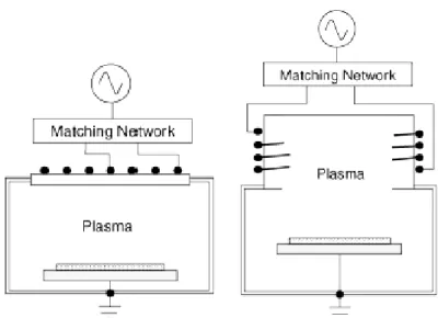
Inductive Coupled Plasma (ICP) sources ………...
3.2.1 Equivalent circuit model………..
3.3
Low Energy Plasma Enhanced Chemical Vapor Deposition
(LEPECVD)……….
3.3.1 LEPECVD reactor at University of Ferrara ………….
CAP 4
Wafer Heating Stage Thermal Model….………
4.1
Wafer Heating model………...
4.1.1 Radiative Heating Model………..
4.1.2 Wafer temperature uniformity……….………..
4.1.3 Contact Thermal Resistance (CTR)………..
4.2
Temperature Measurements………..
4.2.1 Pyrometry……….
4.2.2 Thermocouples (TCs)…..………
4.3
Silicon and Si
1-xGe
xradiative properties……….
4.3.1 Silicon radiative properties model……….
4.4
Wafer optical properties………...
4.4.1 Coherent Formulation………
4.4.2 Incoherent Formulation….……….
4.4.3 Surface roughness effects………..
CAP 5
Thermal FEA results……….……….
5.1
LEPECVD Heating Stage……….
5.2
Experimental Temperature Measurements ………..…………..
5.2.1 Pyrometer measurements……….
5.2.2 Instrumented Wafer measurements……….
5.3
Wafer radiative properties calculation………
5.3.1 Lighly doped Silicon wafer.………
5.3.2 Heavily doped Silicon wafer.……….
5.3.3 Integrated optical properties ………
62
63
66
68
79
79
79
83
85
85
86
88
88
90
97
98
100
102
117
117
119
119
121
122
122
123
123
11
5.4
Numerical Model………..….
5.4.1 Heating element FE model………
5.4.2 Complete Heating Stage FE model……….
CAP 6
LEPECVD deposition results……….…..…...
6.1
Sample preparation………..
6.2
LEPECVD characterization………..………
6.3
Ge/Si virtual substrates (VSs).………..
6.3.1 LT seed layer growth………..……….
6.3.2 High temperature (HT) step growth………..
Conclusions………..
125
126
130
143
143
144
147
148
153
164
13
CHAPTER 1
Introduction
1.1
Ge virtual substrate (VSs)
The heteropitaxy of highly mismatched structures involve many physical aspects which influence the growth mode of the epilayer. The different surface energies between the film and the substrate mainly determines the behavior of the growing film mode. The presence also of the elastic strain inducted by the lattice mismatch and the kinetic processes involved during non-equilibrium epitaxial growth, cause the growth to deviate from ideal equilibrium conditions. In case of Ge/Si heteroepitaxy, the difference in thermal expansion coefficient between Silicon ( 2.6 x 10⁻⁶ °C-1 ) and Germanium ( 5.8 x 10⁻⁶ °C-1 ) cause the
wafer to bend and eventually cracks within the epilayer which can compromise the subsequent overgrowth of electronic devices onto the layer surface. This effect in particular is enhanced in thermally driven CVD epitaxial processes, in which high growth temperature are require in order to overcome the activation energy for precursor scission. Thus development of low temperature epitaxial processes are mandatory, in order to suppress temperature effects and kinetic growth processes and thereby obtain high-quality strain-relaxed epilayers with abrupt interfaces. The high effort in controlling the epi-growth of highly mismatched superlattice structures is justified by the huge potentiality which these structures can offer.
In the field of Silicon – Germanium compounds, one of these potential implications is represented by the creation of high-quality strain-relaxed intermediated Ge layers buffer which can accommodates the lattice mismatch between the underlying silicon substrate and the final epitaxial layer. The idea is to concentrate the MD consequent to plastic strain
14
relaxation within the intermediate Ge epilayer, while suppressing the TDD at the surface. The goal is thus to create a buffer layer which exhibit structural properties closer to a bulk material, acting thus a virtual substrate (VS) for the subsequent film overgrowth. In the last few years. strain-relaxed Si1-xGex VS have been employed into strain-engineered
microelectronic devices (HFET, BiCMOS) in order to enhance the electrical transport properties of Si. The most important application for pure Ge VS is represented by a cost-effective integration of III-V alloys with silicon substrate. In the optoelectronics field this would allows for example the integration of complex optoelectronic devices onto single silicon chip enabling system-to-system communication. In the work of Liu et al. [1.1] a InAs/GaAs quantum dot laser diode grown monolithically onto a Ge VS, shows performances closer an equivalent homoepitaxial laser diode. On the other hand, this can enable the integration of high-efficient III-V concentrator solar cell using low-cost silicon substrate for low-end application.
To be effective, the intermediate layer should exhibits several structural properties which can ensure high-quality film overgrowth. First, the buffer VS must be ideally fully strain-relaxed in order to match as closely as possible the lattice spacing of the overgrown film and avoid elastic strain which would eventually result in either plastic relaxation or surface corrugation. Furthermore, the TDD at the surface must be as low as possible in order to avoid the worsening effect of TD minority carrier recombination on the electrical performance of the device. The electrical transport properties of overgrown GaAs film onto Ge substrate are not sensibly influenced below a threshold value which is a function of dopant concentration of the GaAs layer and generally has a value in the range 104 – 105
cm-2. Finally, the VS buffer film should exhibit low surface roughness in order to achieve
abrupt interface between the buffer layer and the overgrown film. Contrarily, the electron scattering and recombination at the interface can reduce the electrical performances of the overgrown device.
In this work, Ge virtual substrate have been grown onto Silicon wafer using the innovative reactor LEPECVD, which has been developed at the University of Ferrara in collaboration with Dichroic cell S.r.l. Several technical advantages have been exploited in order to obtain high quality intermediate Ge buffer layer with a cost effective solution. Contrarily to other epitaxial techniques, the low energy plasma enhanced CVD reactor shows a high growth rate independent from the temperature of the substrate while maintaining a high uniformity and high crystal quality of the epilayer.
15
1.2
Organization of the thesis
The reminder of this dissertation is organized as follow. In Chapter 2 the most important aspects of the SiGe and Ge heteroepitaxy are reviewed. In Chapter 3 are discussed the main aspects of the plasma deposition process are reviewed. Since the critical aspect of the substrate temperature play a determinant role during epitaxial process, in Chapter 4 are discussed the main aspects of the radiative heating of the wafers, and a theoretical approach to the radiative modeling of silicon wafer have been followed. Finally, in Chapter 5 and 6 are discussed respectively the results of the numerical approach developed in order to improve the LEPECVD heating stage and the results of deposition processes of Ge virtual substrates.
16
Reference
17
CHAPTER 2
Silicon – Germanium epitaxy
2.1
Si
1-xGe
x/Si heterostructures
Silicon and Germanium are completely miscible for any concentration value. The product is a Si1-xGex alloy which have the same zincblende crystalline structure of the two
components, but with a lattice constant that monolitically increasing from that of
Silicon ( 0.5431 nm) to that of Germanium ( 0.56575 nm). The lattice constant
of Ge is 4.18 % larger than that of Si, and for Si1-xGex alloys it does not exactly follow the
linear approximation of the Vegard’s law. The relative change of the lattice constant as a function of the atomic Ge content is given by [2.1]
while the application of Vegard’s law overestimate the lattice parameter up to 12% for low contents [2.2]. Due to larger lattice constant, a Si1-xGex layer with > 0 grown onto a
silicon substrate experiences a compressive stress which depends both on the mismatch between the two lattice constants and the thickness of the layer. In this conditions the film structure is pseudomorphic, i.e. with the in-plane lattice constant of the film fitted
to that of the substrate by a biaxial film stress which results in a tetragonal distortion of the cubic lattice cell of the film along the direction perpendicular to interface. Pseudomorphic film are also called strained film or coherent films. Supposing an isotropic properties of the substrate surface, the strain components of the pseudomorphic film can be expressed as
18
where is the lattice mismatch between the layer and the substrate, and is the Poisson’s number which varies between the value for pure Ge 0.273 and that for pure Si
0.28. The main challenge in the optimization of the epitaxial process of Si1-xGex alloys,
especially in high Ge content layers, is represented by the non-linear increasing of the energy content of highly strained films. The energy of a homogeneous strained pseudomorphic film can be infact expressed as
where is the shear modulus expressed in energy per unit square. Thus a pure pseudomorphic Ge film delivers 100 times the energy compared to a 10% Ge content Si 1-xGex films. Upon a critical thickness , the strain energy reaches a valued for which it
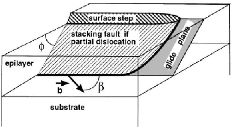
become energetically convenient to release the strain plastically through the formation of misfit dislocations (MDs) which reduce the in-plane stress. For zinblende and diamond crystalline structure materials, the strain is relaxed by the generation of a 60° MD dislocation in the (110) direction and a threading dislocation (TD) arms which extent along the (111) glide plane up to the film free surface, which is schematically show in Fig. (2.1). The orientation of the Burger vector for TDs indicates that while the TD itself does not relieve strain, TD glide and lengthening of the MD segment at the interface does provide strain relaxation. The relaxation degree of the layer defined as the reduction of the in-plane stress can be expressed for a network of MDs with parallel line vectors as
where is the effective Burger vector length, which in a typical Si(100) surface with 60° dislocations in (111) glide planes results , and is the mean MD distance. The parameter value ranges from for complete relaxed layer to for pseudomorphic layers ( ) and results directly proportional to the sum of the MD length at the interface. The value of residue elastic strain results infact approximately the
19 same in layers with a high density of sessile ‘short’ MDs and layers with a low density of extended MDs [2.3]. Obviously, the threading dislocation density (TDD) is lower in the second case. The relaxation process also depends strictly both by the epitaxial deposition processing and the lattice mismatch. Direct epitaxy of large mismatched systems, such as Si1-xGex/Si with a high Ge content, results in uncontrolled lattice relaxation, such as
three-dimensional growth and the introduction of large number of immobile MD and TDs. The results is a near completely relaxed film containing TD density (TDDs) of greater than 109
cm-2 [2.4]. However, for lower mismatch systems ( 1-1.5% ), the incorporation of
strain is more controlled and predominately results in the formation of 60° misfit dislocations at the interface and the associated TDs [2.5, 2.6].
2.1.1 TDD influence on layer electrical performance
The high effort toward obtain relaxed epitaxial heterostructures with low TDD is due to their strong influence on the electrical performance of the grown layer. Since the TD penetrate the epitaxially grown device layer, it acts as a site of localized recombination for the free-carrier reducing the minority carrier diffusion length and minority carrier lifetime. The reduction in the diffusion length and carrier lifetime as a function of the TDD can be calculated using the work of Yamaguchi et al. [2.7], in which it is evaluated the influence of the TDD on the single-crystal thin-films AlGaAs/GaAs/Si double heterostructures (DHs) solar cells performances. First, the process of carrier diffusion toward the TD can be expressed using the differential diffusion equation for the carrier concentration . The diffusion coefficient is related to the minority carrier mobility using the Einstein relation
where is the Boltzmann constant and is the carrier electrical charge. It is also assumed that the single TD has an occupation volume given by , where represents the radius at which the TD have influence on the carrier concentration. Within this radius also, it is also assumed a zero carrier concentration, i.e. no spatial concentration gradient is present from the centre of the dislocation to the radius . Finally, the carrier concentration at distance is assumed being independent from the time and has a value of . Using these approximations, the differential equation of
20
diffusion can be solved by means of the separation of variable and the resulting excess minority carrier concentration can be expressed as
Since they are characteristic values, it is possible to express the total diffusion length and lifetime including the maximum values and for a particular semiconductor
material at a given doping concentration from all other contribution (Shockley-Read-Hall, Auger, band-band, etc. ) in absence of TDs
Based on this model, a decrease in and is expected with increasing the TDD. In Fig.(2.2) are presented the calculated carrier diffusion length and lifetime for different diffusion constant of pure Germanium and GaAs as a function of the TDD dislocation density. The calculation have been performed assuming a minority carrier lifetime value 2.5
x 10-3 s-1 and
5 x 10⁻⁹ s-1 [2.67], a minority electron mobility 3.9 x 10³
cm2V-1s-1 (i.e. dopant concentration 2x1015 cm-3 at 300 K) [2.68] and
7450 cm2V
-1s-1 (i.e. dopant concentration 3x1015 cm-3 at 300K). As expected, the both the minority
carrier lifetime diminishes as the TDD increase following an exponential behavior. Within the TDD range of 104 – 107 cm-2, the Ge minority carrier lifetime is strongly influenced by
the TDD, experiencing a drastic reduction of the value from about 100 ns to 0.1 ns.
Within the same TDD range instead, the GaAs carrier lifetime reaches an asymptotic
value for TDD lower than about 105 cm-2, which means that the electrical properties of GaAs
epilayers with a TDD lower than the threshold value are not influenced by the presence of dislocations. Below that TDD limits, the electrical properties of a heteropitaxial GaAs layer can be thus assumed equivalent to that of bulk GaAs. In the field of concentrator photovoltaics (CPV) solar cells for example, a strain-relaxed Ge virtual substrate with low TDD can be thus in principle to integrate high efficiency III-V alloys with low-cost silicon substrate. A DH
21 layer is grown onto a strain-relaxed graded SiGe virtual substrate (VS) layer [2.69]. In this work is infact proved that a suppression of the TDD in the GaAs layer below the threshold value can lead the solar cell performances to approach closely to these of homoepitaxial GaAs solar cells.
2.2
Critical thickness
2.2.1 Equilibrium theoretical formulations
The growth of coherent tin layers on the rigid crystalline substrate is possible when biaxial compressive or tensile strain in the layer accommodates the lattice mismatch between the film and the substrate material. When the stored strain energy exceed a certain threshold, the heterostructures become metastable and the film strain may give way to MDs. Various theoretical approach have been developed in order to predict the critical thickness as a function of the lattice mismatch and most of them are derived at equilibrium conditions [2.8]. The model developed by Matthews and Blakeslee [2.9, 2.10] is the most often used theoretical approach for critical thickness calculation of heteropitaxy structures. Here it is considered that a preexisting TD in the substrate replicates in the growing epilayer and can bend over to create a length of a MD in the interface once the critical thickness is reached. As the growth of the layer proceed, the dislocation line tension increase and the same does contemporary the resolved force on the glide plane. Thus, the critical thickness is derived by equating the two opposite force and solving for the layer thickness
where is the Burger vector, is the angle between the Burger vector and the line vector for the dislocations and is the the angle between the Burger vector and the line in the interface plane that is perpendicular to the intersection of the glide plane with the interface. Applied to the Si1-xGex/Si heteropitaxy, it is assumed and
which correspond to 60° dislocations with (111) glide systems. For
a Si0.9Ge0.1 epilayer grown onto a silicon substrate, Eq. (2.11) delivers a critical thickness
21 nm, which is high enough to allow SiGe base layer in an HBT. In Fig. (2.4) are summarized the calculation results for the SiGe/Si (100) superlattice obtained by Eq.
22
(2.11) and two other equilibrium models developed by People and Bean [2.11] and van der Merwe [2.12] which are briefly presented below, compared to experimental data retrieved from SiGe/Si (100) heteropitaxy from different works [2.13, 2.14]. The Matthews-Blakeslee model is in good agreement with the most reliable experimental results. The experiments however present a small scattering and some of the results agree with the People and Bean model. This last and the van der Merwe models derived the critical thickness value by comparing the energy gained from a epilayer expressed by Eq. (2.3), and the energy of a dense network of MDs at the interface, differing each other by the assumption of the mean distance between the MDs. Both assumption made are however not physical. In the People and Bean model for example, is assumed a MD spacing of which corresponds to a fully relaxed layer of and so this model should overestimate the value for heteropitaxial systems with a mismatch less than 6.7%. Thus the agreement of this model with some experimental results can be addressed to the finite experimental resolution, which cause an overestimation of the critical thickness value due to onset sluggish lattice relaxation [2.8].
2.2.2 Experimental evidences
Otherwise, the pioneer works of Kasper [2.15] and Bean [2.16] in the field of SiGe systems, shows that under some growth conditions strain in the films above a critical thickness predicted by equilibrium theories is not measurably relieved. They can prove infact with molecular beam epitaxy (MBE) at rather low temperatures of about 550°C, that the experimentally obtained value of the critical thickness are far larger than the equilibrium ones. Only above a second critical thickness does measurable relief occur and even then, the amount of relief is not in accord with the equilibrium theory. They undergo a transition from brittle material at room temperature to a ductile material at temperatures higher than 900°C. At these high temperatures it is possible to find the equilibrium values but at lower values with increasing of brittleness of the material the onset of plastic deformation shift to higher thickness because of kinetic limitations to dislocation nucleation and movement [2.21]. The metastable regime is roughly limited by an experimentally fitted curve on the values found by several measurements [2.17]
23 Even higher critical thickness are possible with growth temperatures below 550°C. This region is called ultrametastable regime [2.18]. Metastable layers capped with silicon withstand temperature treatments during device processing and allow the design of SiGe-HBTs with the frequency limits beyond 200 MHz [2.19]. On the other hand, the works of Fritz [2.20] and Dodson and Tsao [2.21] suggests that the observed metastability can be explained by sluggish plastic deformation rates accompanied by a finite experimental resolution and that the second critical thickness is that for which strain relief is just sufficient to be observable. Vogg et al. [2.22] report also a slight increase the critical thickness of the Si0.77Ge0.23/Si (100) heterostructure by a chemical treatment of the Silicon
substrate surface with gaseous HCl at temperature up to 800°C before the CVD deposition process. In Fig.(2.5) are compared the XRD scan curves retrieved for different layer thicknesses with and without the pre-process chemical etching. The thickness range have been choose in order to be compared to the equilibrium critical thickness for this
epitaxial system, i.e. about 170 nm. The non-etched sample start the relaxing process at 178 nm, slight after the predicted equilibrium critical thickness, while the XRD scan for the etched ones shows interference fringes up to 216 nm, which result about 27% larger than the value. The presence of the interference fringes in the measured suggest that
negligible incoherent scattering due to the presence of MD and TD in the layer have occurred, and thus it can considered as pseudomorphic. Furthermore, the diffuse scattering evaluated with the XRD In particular, the etched 259 nm thick sample show a degree of relaxation which is comparable with that of 174 nm non-etched sample. The evaluation also of the etch pit density on treated sample show a TDD lower than 1.7x10⁻⁴
cm-2, which confirms the retarded relaxation in case the chemical treatment is applied.
2.2.3 Kinetic theoretical formulation
The equilibrium theoretical formulation results described in Section 2.2.1 are thus capable to predict the critical thickness value in heteroepitaxial systems as function of the lattice mismatch, only if the epitaxial deposition is performed at temperatures high enough to activate the dislocation glide processes. However, measured critical thickness for epilayers grown using lower temperatures show that it is possible to obtain metastable heterostructure with thicknesses far larger than the predicted ones. Beanland [2.23] proposes a modified model of the Matthews-Blakeslee approach in which different dislocation generation processes are taken into account. In particular, the Frank-Read and the spiral dislocation multiplication processes, which have been experimentally observed
24
in Si1-xGex/Si system by LeGuoes [2.24] and Capano et al. [2.25], are included into the
model. In Fig.(2.6) is presented a possible configuration for the Frank-Read source in a heteropitaxial layer. First, a TD pinned between the two point A and B is considered. With applied stress, the dislocation bows out between A and B, until it reaches the free surface of the epilayer. At this point, the bowing loop break into two dislocations and finally the interaction of the two dislocation results in the formation of a half-loop as shown in Fig.(2.6)d. This process leaves the original dislocation intact, and it can participate in further multiplication. For this mechanism, the critical thickness calculation is performed balancing the resolved stress on the pinned dislocation and the dislocation line tension, depending thus by the position of the pinned points and the orientation of the pinned segment. Assuming that the AB pinned segment lies along the <112> direction, the minimum thickness for which the Frank-Read source may operate is given by
where is the Matthews-Blakeslee contribution calculated using Eq. (2.11). Similar considerations can be derive for the dislocation spiral multiplication processes. It is assumed that a TD is pinned at a single point A and a stress is applied. In Fig.(2.7) are presented the schematical representations of the spiral multiplication process. With the applied stress, the dislocation may bow out above the pinning point. The bowed section continue to expand and may glide to the interface to relieve the mismatch strain. Further expansion of the bowed portion may lead to production of a half-loop if the bow reaches the surface and split in two as in Fig. (2.7)d. In this case the calculation of the critical thickness have similar expression of Eq. (2.13) but with the factor substituted by the
term, which depends by the height of the pinned point within the epilayer. In Fig. (2.8) are plotted the results using the equations of the two generation contributions. The Frank-Read contribution results in general four to seven times the Matthews-Blakeslee critical thickness values while the spiral source can become active at two to four time the term. It is therefore likely that both mechanisms are active in relaxing SiGe/Si heteroepitaxial layers.
On the other hand, Dodson and Tsao [2.21] propose an explanation of extended metastability of SiGe epilayers by means of a strain excess, which is necessary for the film
25 relaxation. Similar to the Matthews-Blakeslee theoretical approach, a balancing of the force action on the dislocation and the consequent opposite force due to elongation in performed. However in this case, the opposite term has been evaluated as
which is balanced with the resolved shear stress resulting in a excess stress which can be expressed as
which represent the measure of the driving force for strain relief and hence both for the deviation from equilibrium and for the degree of metastability. Thus the experimentally fitted Eq. (2.12) can be explained as a ‘ isobar ‘ of excess stress . So if this excess
stress is greater than zero, then there is a net force for dislocation motion. In case is less or equal to zero, there is not net force driving dislocation motion, and the excess stress isobar curve equals the Matthews-Blakeslee curve derived with Eq. (2.11). Even in case of positive stress however, the dislocations do not necessary move freely. On a give experimental time scale, there must be enough excess stress to lead to observable plastic deformation. In Fig.(2.9) are presented the theoretical results of this approach and the measured critical thickness for different samples with increasing lattice mismatch and same growth temperature of 494 °C. In the case of Si1-xGex/Ge, the authors identify the
as the maximum excess stress for metastability at the 494 °C growth
temperature. The transition also from metastability region to the partially relaxed state is well defined by the ‘isobar’ curve. Furthermore, the excess stress for a particular heteoropitaxial system depends strongly for the temperature of wafer processing. In Fig. (2.10), the excess stress for the Si1-xGex/Ge have been plotted as a function of the
growth temperature. Films grown at temperatures comparable to the 494 °C value, show a critical stress very similar to the value derived earlier, with a definite
trend towards higher critical excess stresses at lower temperatures. This trend is consistent with the expectation of generation of sessile MD and TD at lower temperatures, and so they require a greater driving force in order to move at comparable rates. At higher growth temperature instead, films shows a significantly lower
26
values, which suggest that a change in the plastic relaxation mechanism have been happened. The plot in Fig.(2.10) can also be used as a deformation-mechanism map [2.26].
2.3
Si
1-xGe
x/Si growth modes
In heteroepitaxy deposition processes, an adsorbate material is deposit on the substrate which is a chemically different material. At equilibrium, the stability of the epitaxial layer free surface depends mainly on the balance of the free energies of the surface and interfaces for the substrate and epitaxial layer [2.27]. A planar surface is stable if it minimizes the free energy. Alternatively, the minimization regards the difference between the free-energies of a state with deformed surface and of the with planar surface, and the same mass of adsorbate and substrate. The difference must be positive for all deformations in case the plane surface is to be stable [2.28]. If the elasticity is ignored, the stability condition of a plane interface is given by the well known Young’s relation , where is the free energy per surface area at the substrate-gas
interface, is the free energy per surface area of the substrate-adsorbate interface and
is the free energy per surface area of the adsorbate-gas interface. During the lattice
mismatched epitaxial deposition processes otherwise, the elastic energy and the other processes due to the kinetic altered the equilibrium state causing 3D growth even in case of wetting epitaxial layer. In Fig. (2.11) are schematized the three main typologies in which the epitaxial layer can growth. The 2D Frank van der Merwe (FM) growth on a flat substrate is characterized by the nucleation of successive monolayers which cover the substrate surface. The 3D Volmer-Weber (WB) growth instead involves the development of isolated island on the substrate, followed by their growth and coalescence. Finally, the 2D-3D Stranski-Krastanov (SK) growth, the process proceeds in 2D growth but becomes 3D in nature after the growth of a certain critical layer thickness.
2.3.1 The Asaro-Tiller-Grinfeld (ATG) instability
Once the Si1-xGex epilayers is grown onto the lattice mismatched silicon substrate, the
elastic strain energy gained through the deposition process can be release plastically by the introduction of a dislocation or elastically by tetragonal distortion along the direction perpendicular to the interface. However, even if the layer growth is coherent and in equilibrium state, it is found experimentally that the mismatched epitaxial film can stand
27 the elastic energy by deforming the free surface and thus moving from 2D to 3D growth mode, named ‘ 2D – 3D transition ‘. If the misfit is moderate, this deformation leads to alternating hills and valleys, while for stronger misfit as in the case of Ge/Si heterostructure, the adsorbate film split into clusters. The quantitative calculation of the deformation of the epilayer surface at the equilibrium have been developed by Asaro and Tiller [2.29] and later in detailed by Grinfeld [2.30]. In this theoretical approach, the free energy of a sinusoidal modulation of the film surface is evaluated compare to a flatted one. The modulation height of the surface can be described as
where is the height in case of flat surface and and the amplitude and phase of the modulation. The terms regarding the free-energy change due to the elastic energy can be expressed as
where and are two elastic constant of the epilayer, is the Young module of the film and is the surface area. Thus the elastic free energy change resulting from the sinusoidal deformation is negative. However, the increase of the surface area due to modulation opposes to the elastic free energy gain. This component can be expressed as
, where the is coefficient of surface stiffness. By minimizing the total free
energy, expressed as the sum of the elastic and surface tension component, it is possible to derive the wavelength of the surface modulation above which the surface is stable
The instability of coherent epitaxial films have observed in the growth of pure Ge on Si(111) and [2.31] and and on Si1-xGex on Si (100) systems [2.32], while pure Ge on Si
(100) this process lead to split in cluster for thickness larger than three-monolayers [2.33].
28
2.3.2 Si1-xGex/Si kinetical growth modes
At equilibrium, the growth modes phase diagrams can be derived as function of the lattice mismatch, and in case of SiGe heteroepitaxy systems, as a function of the stechiometric composition of the epilayers. In Fig.(2.12) are presented the phase diagrams for the Si 1-xGex/Si systems calculated by Nakajima et al. [2.34] in case plastic relaxation by
dislocation is either considered or not. The calculations are performed at the equilibrium, and thus it results from the comparisons of the assessed strain, surface and interface energies for the three different growth modes as a function of the Ge content. Since kinetics processes are neglected, the diagrams are derived supposing a ambient temperature of 27 °C as a the temperature increase does not affect significantly both the strain and the free energies [2.34]. From the results it is clear that when the concentration in small, namely under the value 0.5, the FM mode is dominant up to the maximum calculated value of 8 ML. As the mismatch increases, both the strain and the interface energy increase also and the 3D growth modes are favored. For the pure Ge onto Silicon, the SK growth mode is energetically favored even after 1 ML adsorbed. In case the plastic relaxation is considered, the SK and VW growth modes regions shrink due to a reduction of the strain energy, and thus the FM modes is favored at slight increased mismatch values.
However the conditions experienced in crystal growth by Plasma Enhanced CVD processes are far from being at equilibrium. The most kinetic factors which influence the growth mode and surface morphology are the surface diffusivity and the flux of impinging adatoms. During epitaxy, these two processes can be tuned by modulating the temperature and the growth rate respectively. In addition to that controllable factors, the presence of terraces due to substrate surface off-cut and the Ehrlich-Schwoebel (ES) [2.35] barrier to diffusion step can play a determinant role on the growth mode. Furthermore, the presence of a surfactant can modify the free energy of the surface, promoting thus either 2D or 3D island growth [2.8]. In considering the kinetic parameters in order to obtain a FM or step-flow (SF) growth, Tersoff, Denier van der Gon and Tromp (TDT) [2.36] developed a theoretical model which relate the growth modes to temperature, adatom flux and substrate miscut parameters. In particular, for a given values of temperature and adatom flux, the theoretical approach assess their influence on the island nucleation processes on the substrate surface. After the incoming adatoms are adsorbed on the substrate surface, they can diffuse, re-evaporate or eventually interact
29 with other adatoms creating clusters. The formed cluster are stable as soon as the critical dimension which minimize the surface energy has been reached [2.8]. From this point, the subsequent adsorbed adatoms which impinge on substrate surface can diffuse and combine with the stable clusters increasing the island dimension, while adatoms which impinge on the top of the first island layer can either surpass the ES barrier or create a new stable cluster. Thus, in case the first monolayer clusters coalesce before new cluster are created on the second monolayer the growth proceed as layer-by-layer. Otherwise, the epilayer growth experiences a kinetic roughening.
Based on an atomistic approach, the model assumes a nucleation rate expressed as where is the diffusivity for surface atoms, is the surface atomic density expresses as atoms per unit area, is the normalized dimensionless adatom density and is the number of adatoms by which is composed the critical cluster. Then the differential diffusion equation is evaluated at the first monolayer and upon the fist monolayer island, for which the probability of overcome the ES barrier at the boundaries is expressed as , where is a constant, is the ES barrier and is the activation energy for surface diffusion on the top of the island. Afterward, it is then possible to calculate the fraction of islands which have nucleated a second layer on their top by solving a first-order time-differential equation in which the total nucleation rate upon a island, assessed integrating the rate over the island surface, is taken into account. The solved expression can be expressed as
where is the radius of the island, is a dimensional parameter which depends on the critical cluster size, and is the critical radius for a second layer nucleation for the transition from FM to SK growth. Two expressions can be derived for the in case the influence of the ES barrier is either neglected or not. The derived expressions can be described as
30
where is the impinging adatoms flux, is the separation between the nucleated islands, is a length that characterized the diffusion barrier at the edge of the islands and , , , are constants function of . In Fig.(2.13)a is plotted the Eq. (2.20) as a function of the medium island radius for different values of the parameter. Essentially, if there is an high probability of new nucleation on the islands before they coalescence. This give rise to undesirable surface roughening in the homoepitaxy or heteroepitaxy and thus the epilayer experience a SK growth. Otherwise, the island can coalesce and the growth results FM. The model can be also used to understand the growth behavior as a function of the temperature, as the and can be expressed as a function of the temperature.
The model takes into account also of the offcut by the parameter which depends on the miscut angle and the height of the vincinal steps. With a sufficiently high temperature or step density and in this case adatom can diffust to the surface steps before nucleating new islands. The grwth thus proceed as step-flow (SF). At lower temperature, so the growth mode will be layer-by-layer (FM), whereby islands nucleated and then coalescence. At still lower temperatures, so that multilayer (SK) growth will result. The model also can explain qualitatively the observation of reentrant layer-by-layer growth [2.37], in which the growth mode at high and low temperature differs from that at medium temperature range. The model results describe well the STM observation of pure Ge growth onto an off-cut Silicon substrate [2.38] almost qualitatively as it does not take into account the surface reconstruction as a function of the temperature which generate a anisotropical diffusion of Ge adatoms on the surface, or the presence of a surfactant which modify the free energy of the surface. Anyway, the TDT model is useful in order to understand qualitatively the behavior of lattice growth during the epitaxy processes.
2.4
Ge/Si integration
A real challenge is represented by the integration of high content Si1-xGex layers onto
Silicon (100) substrates. As describe earlier, the high lattice mismatch of 4.18% for pure Ge results in a critical thickness than is less than 1 nm and in an uncontrolled plastic relaxation characterized by a high number of dislocations which interact and cause an high TDDs at the interface. The high elastic energy gained even after few MLs, induce the epilayer to split into clusters whose dimension and orientation depends on the cluster
31 volume and the growth temperature [2.39]. This change in creating an high density of localized nanostructures (109 – 1011 cm-2) are gaining much attractiveness as they can be
used as quantum dots (QDs) or seed for self-organized device classes [2.15]. A stacked sequence of Ge islands have been successfully employed as intermediate layer into a p-i-n Silicon solar cell in order to enhance the performance of the cell in the near-infrared regime [2.40]. On the other hand, relaxed Ge epilayer with low TDDs can be used as a virtual substrate (VS) for III-V alloys integration with low cost silicon substrate in the field of the optoelectronics [2.41] and high-efficiency concentrator photovoltaic (CPV) solar cell [2.42]. Below, a brief review of the issues and literature works on the Ge/Si epitaxy is presented.
2.4.1 H2
influence
It has been recognized the function of the atomic H2 in the Ge/Si heteroepitaxy system as
surfactant [2.43 – 2.44]. Surfactants are surface-segregated impurities, which have a number of applications in heteroepitaxy and engineered hererostructures. Surfactants may alter the growth mode for heteroepitaxy by modification of the surface energies for the substrate or the epitaxial layer, if the growth mode is determined by thermodynamics. Alternatively, a surfactant may change the surface diffusivities or the energy barriers at the edge of the islands, if the growth mode is determined by kinetics [2.8]. During CVD processes, molecular or atomic hydrogen is naturally generated by the scission of the gas precursors, such as GeH4 or SiH4, or either injected into the reactor as surfactant. By using
UHV-CVD deposition at temperatures lower than 400°C, the introduction of a relative low partial pressure of H2 results in a great enhancing of the surface diffusivity and thus an
extended layer-by-layer growth at thickness for which 3D growth are expected [2.43]. In Fig. (2.15) the RHEED analysis are presented as function of the temperature and H2 partial
pressure. Best enhancing is found at lower temperature of 100 – 300 °C, in which the extended RHEED oscillations indicates a FM growth, while at higher temperatures, no difference can be found by the comparison with sample grown without the H2 inclusion.
This effect can be addressed to a higher desorption rate of hydrogen which limits the surface coverage. The RHEED analysis confirm a nearly flat surface up to 55 MLs in these conditions, characterized by a 1x1 surface reconstruction. A flatterning effect on Ge(100) surface at 300 - 400 °C have been also reported by Kahng [2.44]. On the other hand, an excess of H2 can generates pin holes within the epilayer as the hydrogen bond more
32
strongly with silicon than germanium [2.44]. The use of hydrogen also have been proved to strongly suppress the Ge surface segregation during Si/Ge/Si overgrowth [2.45].
2.4.2 Defect induced relaxation
In order to avoid uncontrolled plastic relaxation of the pure Ge epilayer, a very thin buffer layer grown at particular epitaxial conditions or treated employing a particular procedure is often used [2.46-2.48]. The idea is to create a thin layer, commonly called seed layer, with a characteristic high vacancy or interstitial defectivity density which accommodate the mismatch and thermal strain between the epilayer and the substrate while suppressing the extending of TDD segment through the epilayer by interaction with the layer defectivities [2.46]. It is infact proved that a high concentration of induced point
defects within the lattice structure can efficiently suppress the extending of the line
defects by pinning during the onset stage of relaxation [2.49]. Once the TD is pinned, the gliding can proceed only if the TD climbs the point defect, and this process promotes the mutual annihilation of TD arms. [2.50]. The introduction of point defects supersaturation within the buffer layer, reduces also the kinetic barrier against dislocation generation, shorten the metastable pseudomorphic growth and provoke relaxation of thinner layers [2.50]. Furthermore, the planar condensation of point defects cause the nucleation of prismatic dislocation loops inside the layer, which may reduce the need for nucleation of dislocation half-loops at the surface [2.51].
Supersaturation of point defects within the buffer layer can be produced by 1 kV Si+ ion
bombardment of the layer suface during the metastable pseudomorphic growth stage [2.50] and by a 25keV implantation of Ar ions onto the Silicon substrate [2.52]. The subsequent overgrowth of a Si0.8Ge0.2 at 500°C and annealing at 900°C allows a very low
TDD density within the epilayer as a dense network of dislocation which generates at the interface promote the relaxation of the epilayer. In this way, the defectivity caused by the plastic relaxation is mostly confined within the volume regions near the silicon substrate surface, thus reducing strongly the TD arms which propagates through the epilayer.
On the other hand, a drastic reduction of the growth temperature can give rise to epilayers with an ordered crystal structure but with a high density of vacancy point defects. This process is mainly due to a strong reduction of the surface diffusivity of the adatoms which impinges on the substrate surface [2.53]. This process is effective only if the temperature substrate is low enough to favor the generation of vacancies in the lattice, but high enough
33 to avoid the amorphous growth of the epilayer. Studies base on Si homoepitaxy also indicate a narrow temperature process window for crystalline epitaxial layer grown at temperature lower than 200 °C [2.54]. This process is also strongly influenced by the adatom flux and thickness of deposited epilayer due to the kinetic growth considerations described in Section 2.3.2. The real challenge is thus a very tight control of the key parameters during deposition, with particular attention to the substrate temperature profiles. After the thin low temperature (LT) seed layer is grown, a subsequent overgrowth step at high temperature (HT) is then performed. Comparing to a constant temperature epitaxial process, the lattice mismatch between the HT layer and the substrate is accommodated by the LT layer, which acts as a VS for the subsequent overgrowth while confining within its volume the plastic relaxation induced dislocations. The drastic reduction of the TDD and in-plane strain also play a decisive role in reduction of the surface roughness. The multi-step growth have been applied successfully by Bauer
et al. [2.46] to the SiGe/Si system in order to obtain strain-relaxed VS with thickness
under 0.1 . The first step growth parameters are calibrated as a function of the Ge content, while the thickness slight exceed the equilibrium critical thickness predicted by the Matthews-Blakeslee theory. The subsequent HT growth is performed at 550°C until the People metastability thickness defined by Eq.(2.12) is reached. In Fig.(2.16) are presented a TEM imaged comparison between a standard constant temperature and LT-HT combination growth. While the standard growth creates strain pseudomorphic layers, the temperature modulation growth allows to obtain epilayers with a relaxation 90 – 100% and virtually free of TDDs. Zhou et al. [2.55] uses a LT Ge seed layer grown at 350 °C onto Silicon (100) substrate and a subsequent HT at 600°C. By this way, a thin VS with a relaxation factor of about 99% and a TDD of 5x105 cm-2. The root mean square (RMS)
roughness of the epilayer surface has been evaluated as 0.7 nm. Although the good results, the growth rate is lower than 1.17 nm/min for the HT layer, while it results as low as 0.58 nm/min for the LT seed layer. This results in a overall deposition time of about 4h. A similar processes have been used by Shin et al. [2.56] and Olubuyide et al. [2.57] which studies the impact of a LT seed layer on the roughness and TDD for a Ge/Si heteropitaxial system while modulating the substrate temperature within the range of 330 °C and 350 °C. Even in this case, a very narrow temperature window process is identified, as LT layer grown for temperature higher than 350°c lead to a surface roughening due to enhanced adatom mobility, while for temperature lower than 330°C too many defects are generated. At the optimal value of 335°C, an onset 3D growth is observed which instead become more smoother as the deposition process proceed due to coalescence of the islands.
34
Furthermore, in case a temperature ramp is set between the LT and HT layer growth, a slight increase on the overall surface roughness can be achieved. Finally, a very smooth pure Ge layer with a RMS 1.9 nm and a TDD of 2x107 cm-2 is obtained using a 30 nm LT
seed layer grown at 335 °C and a HT temperature ramped layer.
Other techniques employed in SiGe/Si epitaxy for TDD and surface roughness suppression involve the use of continuously or stepwise graded SiGe buffers [2.58], thick graded buffers with following chemical-mechanical polishing [2.59], H or He implantation with formation of bubbles below the interface to direct the dislocation arms beneath the layer itself [2.60] and compliant substrates in order to use the higher plasticity of the material for TDD reduction [2.61].
2.5
Layers characterizations
A wide variety of techniques were used to characterize the epitaxial films and structure developed. These comprehend surface roughness, composition, layer thickness, defect density and residual strain.
2.5.1 Atomic Force Microscopy (AFM)
The quantification of the surface rougheness has been conducted using an Atomic Force Microscopy (AFM) characterization. A quick surface scan with a stylus allows for accurate determination of the surface roughness, as shown in the example of Fig.(2.16) of a Ge/Si (100) sample grown at 570 °C. Built in analysis tools are employed to determine the root means square (RMS) roughness and the maximum peak-to-valley heigh. The main drawbak associated with this technique is that it samples a very small are of the wafer surface, typically a square are ranging from about 1x1 to 50 x 50 , so several assessment of the surface RMS have been conduct in different part of the sample as to evaluate the epilayers surface uniformity. The entire set of measurements conducted in this work have been performed using a Nanoscope III Digital Instruments in contact mode configuration.


![Fig. 2.14 Regimes of kinetically controlled growth modes for various values of temperature and substrate miscut angle [2.36]](https://thumb-eu.123doks.com/thumbv2/123dokorg/4709179.45207/49.892.245.640.146.396/regimes-kinetically-controlled-growth-various-values-temperature-substrate.webp)
![Fig. 2.15 RHEED specular intensity oscillations along the [100] azimuth during growth of Ge/Si (100) at 300°C for different partial pressures (a), and for different temperature at 6x10 -6 mbar](https://thumb-eu.123doks.com/thumbv2/123dokorg/4709179.45207/50.892.156.700.174.579/specular-intensity-oscillations-azimuth-different-pressures-different-temperature.webp)