A Cross-Level Verification Methodology for Digital
IPs Augmented with Embedded Timing Monitors
Abstract—Smart systems implement the leading technology advances in the context of embedded devices. Current design methodologies are not suitable to deal with tightly interacting subsystems of different technological domains, namely analog, digital, discrete and power devices, MEMS and power sources. The interaction effects between the components and between the environment and the system must be modeled and simulated at system level to achieve high performance. Focusing on digital subsystem, additional design constraints have to be considered as a result of the integration of multi-domain subsystems in a single device. The main digital design challenges combined with those emerging from the heterogeneous nature of the whole system directly impact on performance, hence propagation delay, of the digital component. In this paper we propose a design approach to enhance the RTL model of a given digital component for the integration in smart systems, and a methodology to verify the added features at system-level. The design approach consists of “augmenting” the RTL model through the automatic insertion of delay sensors, which are capable of detecting and correcting timing failures. The verification methodology consists of an automatic flow of two steps. Firstly the augmented model is abstracted to system-level (i.e., SystemC TLM); secondly mutants, which are code mutations to emulate timing failures, are automatically injected into the abstracted model. Experimental results demonstrate the applicability of the proposed design and verification methodology and the effectiveness of the simulation performance.
I. INTRODUCTION
The design of modern embedded systems have become challenging not only for its increasing complexity, but also for its emergent multidisciplinarity. New generation devices, known as smart systems, typically incorporate analog, digital and Micro Electro-Mechanical System (MEMS) components integrated with application-specific sensors and actuators, mul-tiple power sources, intelligence in the form of embedded software [1]. However, current design and simulation method-ologies are not suitable to manage the integration of intrinsi-cally heterogeneous components. The involved subsystems are described using different languages and tools, at different lev-els of abstraction. New efficient co-design and co-simulations methodologies are required to deal with interaction effects between the environment and the system and between the components.
In the digital domain, the design flow is typically based on a top-down approach and is highly standardized (e.g., commercial, fully automated synthesis and optimization tools, technology libraries, etc.)[2] and so are the formats and the models used in these design flows (i.e., VHDL or Verilog). The new challenges in the context of smart systems do not concern the design of the single component (which is already a difficult task). Rather, the integration of multi-domain components in a single device generates further design constraints to be taken into account. Such constraints have to address the interaction effects and, hence, they must be modeled and simulated at system-level.
Transaction Level Modeling (TLM) is the consolidated high-level approach in digital design. Combined with Sys-temC language, TLM facilitates design space exploration and verification of the system functionality without focusing on
Digital IP Metrics Sensor Inputs Outputs Metrics Metrics OK Wrapper
Fig. 1. Wrapping of digital IP and sensors to generate an “augmented” description.
the implementation details. This guarantees a sound trade-off between simulation performance and accuracy for a wide range of user’s needs during the digital component design and verification. Moreover, activity research is working on SystemC-AMS, to model components of different nature at high abstraction levels [3]. This would allow an homogeneous simulation scenario for a multi-domain system.
In this context, tools for the automatic abstraction of existing RTL models represent a valuable support for the design of modern complex systems. Well-known examples are the RTL-to-SystemC abstraction tools for reusing RTL models of IPs [4], [5]. The automatic translation process to TLM preserves only the functionality and timing properties (yet with different accuracy levels) of the original IP. On the other hand, most of the design constraints are related to physical properties of the circuit (e.g., frequency, power supply, temperature). As a consequence, the verification of the additional design constraints is not achievable, at the state of the art, at high level of abstraction (TLM).
Conversely, verification of physical properties related to specific design constraints of a given digital IP at RTL has several limitations:
• the simulation performance at RTL is prohibitive for
reaching high-quality results;
• the manipulation of the RTL code for testing the
system correctness over different metrics values is time consuming and not scalable to large and complex systems;
• the verification of the RTL model, once integrated into
a high-level system description (SystemC TLM) of a smart system requires co-simulation instead of simu-lation, thus decreasing the simulation performance of the whole system platform.
The concept of mixed-level modeling or co-simulation indeed emerged due to the need of efficiency and higher simulation results. It has been applied, for instance, in design exploration and validation [6], RTL fault injections with error propagation at system level [7] and prediction of non-functional properties such as aging [8]. However, the lower level models act as bottlenecks in all these mixed-level approaches, thus slowing down the simulation of the whole system.
Since many physical properties affect the timings of a digital IPs, the use of timing monitors allows to capture all their effects concurrently. Therefore, this paper proposes a methodology for system-level verification of digital IPs augmented with embedded timing monitors. The main con-tributions are the following:
• a design paradigm based on constraints detection and correction to augment the functionality of a digital IP modeled at RTL by embedding timing monitors;
• a verification methodology to abstract the description
of the augmented digital IP to TLM, in order to speed-up the verification of the design paradigm;
• a new class of TLM mutants, which are timing faults
automatically injected into the abstracted IP to verify the correctness of the embedded monitors.
The paper is organized as follows. Section II provides a brief background on constraints detection and correction. Section III describes the implemented design paradigm to augment the digital IP functionality. Section IV presents the cross-level verification methodology for the proposed design paradigm. Section V shows the effectiveness of the presented methodology with some experimental results. Finally, conclu-sions are discussed in Section VI.
II. BACKGROUND ONDETECTION ANDCORRECTION
PARADIGM
The design of a digital component incorporated into a smart system is affected by additional constraints due to the integration of multi-domain subsystems in a single device. Constraints here basically imply the metrics to be considered concurrently [1]. They fundamentally include performance, reliability/robustness, power consumption and temperature. These metrics are directly or indirectly related to specific physical quantities, i.e., frequency (propagation delay), supply noise, supply current, supply voltage and temperature. The direct measurement of such quantities allows to define a design paradigm based on detection and correction of the related constraints.
Consider a generic digital IP modeled at RTL through a hardware description language (HDL), as shown in Fig. 1. For a given metrics, a customized sensor monitors its value by directly measuring the corresponding physical quantity. The sensor provides the metrics value (Metrics output) and signals whether the related constraint is met (Metrics OK output). Morever, it provides a control signal regulating some hardware knobs that attempt to ”correct” the corresponding metrics value. Depending on the given metrics, the robustness of the IP is increased against different design issues.
The scaling process of CMOS technology generated several side-effects. Many of these non-idealities, however, have a direct impact on the performance of digital devices. Process variability makes delay a non-deterministic quantity, so that the actual delay becomes instance-specific [9]. Voltage and temperature variability shift the value of the nominal delay depending on the operating point [10]. Aging effects such as Negative Biasing Temperature Instability (NBTI) or Hot Carrier Injection (HCI), conversely, cause the nominal delay to drift over time [11]. In order to address all these physical effects and enhance the global reliability, dynamic on-chip monitoring of performance is highly demanded.
On-chip delay monitoring architectures proposed in liter-ature mainly differ on the type of measurement performed: Absolute measurement of delay values or check whether a given threshold is exceeded. In the first approach the absolute measurement of path delay is achieved using either a Time-to-Digital Converter (TDC) to translate timing information into digital values [12], [13], [14], [15], or time-to-voltage conversion to translate path delay into voltage levels [16]. In the second approach ad-hoc sampling elements replace latches or flip-flops in the critical paths of the circuit. They detect the occurrence of a timing violation by observing a signal transition within a given time window [17] or by performing a delayed comparison of the monitored signals [18], [19], [20]. Recovery mechanisms are also implemented in order to correct
the detected errors.
Nevertheless, once delay sensors have been embedded into a digital IP, the detection and correction characteristics must be verified. Several solutions based on fault injection can be found in literature [21]. Some techniques rely on simulator commands to easily manipulate model signals or variables without altering the HDL code. However such commands are not standard. Rather, they are restricted to a specific HDL simulator. Another class of techniques modify the original RTL code, either by adding saboteur blocks [22] in the design structure, or by modify the behavior of some components using mutants [23]. Nevertheless both techniques require additional control signals to activate the occurrence of a fault and automatic tools to add/remove the HDL modification.
III. DESIGN OFAUGMENTEDDIGITALIPS FOR
CROSS-LEVELVERIFICATION
The proposed design methodology augments the function-ality of a given digital IP in order to enable its cross-level verification. The constraints detection and correction paradigm introduced in Section II is implemented by automatically inserting appropriate sensors into the IP at RTL level. Since performance is the target constraint, the embedded monitors are timing sensors. As mentioned in Section II, by sensing the propagation delay in appropriate locations of the digital IP, the performance is monitored and optimized to improve the circuit reliability. Once the augmented digital IP has been converted to a high-level model (SystemC TLM), the information on delay is preserved due to the additional functionality implemented by the sensor. This allows to catch the physical properties (e.g., temperature, aging) whose side-effect is to violate performance constraints.
Two essential requirements must be met by the delay sensor implementation to guarantee the cross-level verification of the paradigm: (i) it must be synthesizable, and (ii) it must affect either functionality or timing of the IP where it is embedded. This paper proposes two different architectures for an on-chip delay monitor fulfilling such requirements: an extended Razor flip-flop and a Counter-based monitor. The two sensors can be used individually or in combination, depending on the required level of precision: a generic fail/no fail information or a more quantitative information about the delay of the logic block.
A. Modified Razor flip-flop
The first monitor implementation is based on the Razor flip-flop (FF) concept [18], which has been modified with an additional multiplexer (see upper side of Fig. 2).
It enhances the FF of critical paths by introducing an shadow latch that samples the FF input data on the negative level of the delayed clock signal CLK. Since CLK is delayed
by half CLK period (TCLK
2 ), the Razor working time window
is bounded by the rising and falling edge of CLK (see Fig. 5(a)). The outputs of the FF and shadow latch are compared and an error signal E is asserted in case of timing failure. When the control signal R is high, the recovery mechanism is executed and the error in the faulty FF is corrected. The correction feature can be selectively activated on each modified Razor FF acting on the corresponding signal R.
B. Counter-based monitor
The second sensor implementation is an on-chip counter-based monitor. It relies on a simple counter to measure the propagation delay on critical paths of the digital IP (see lower side of Fig. 2). Compared to the modified Razor FF, it provides an absolute measure of delay through rather than a timing
DIGITAL IP FF C0 FF C1 C2 DATA_IN FF DATA_OUT RAZOR FF R E RAZOR FF R E METRIC_OK SHADOW LATCH MAIN FF 0 1 Q E CLK CLK R MODIFIED RAZOR FF C3 COUNTER OBS_WIN CTRL EN LATCH n LATCH EN EN EN EN n REG n REG 0 1 MEAS_VAL n D
COUNTER BASED DELAY SENSOR RAZOR
FF
R E
CURR_CPS
Fig. 2. Example of digital IP augmented with the implemented delay monitors.
failure detection.
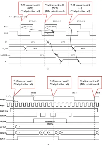
Using an additional clock signal (i.e., HF CLK in Fig. 5(b)) with higher frequency multiple of the clock frequency of the IP (i.e., MAIN CLK), the monitor enumerates the amount of HF CLK periods elapsed for the signal propagation from the path start point to the path end point. The measurement is performed during a predefined time window called observ-ability window (i.e., OBS WIN in Fig. 5(b)) where all signal transitions are captured. The duration of OBS WIN is chosen at design time. Two registers are used to store the counter value on the occurrence of both rising and falling transitions. The delay measure is then selected according to the last captured transition. A control block compares the obtained value with reference values determined at design time.
In general, the main sensor characteristics depend on the HF CLK period. Since the counter is synchronous with HF CLK, the maximum resolution is HF CLK period and the
maximum error is ±THF CLK
2 . The dynamic range depends
also on the length of the observability window, indeed the maximum measurable delay corresponds to the time interval beginning with the first MAIN CLK rising edge (signal transi-tions start to propagate through the monitored path) and ending with the falling edge of OBS WIN (no more signal transitions are captured).
IV. VERIFICATIONMETHODOLOGY
The verification methodology aims at testing the detection and correction paradigm proposed in Section III at TLM. The methodology relies on the following steps (see Fig. 3):
1) RTL-to-TLM abstraction of the augmented digital IP. Given the RTL model of the digital IP and sensor, which are implemented in synthesizable HDL (VHDL, Verilog) at RTL, an abstraction tool is ap-plied to abstract them into SystemC TLM.
2) Injection of mutants in the abstracted digital IP. A set of C++ functions has been implemented to simulate timing delays in the digital IP. These functions, hereafter called mutants, are automatically injected in the abstracted digital IP to verify, during simulation, the sensor correctness.
Automatic Stimuli Generator and Sensor Monitor Digital IP Sensor (metrics X) Outputs Inputs Metrics Metrics_OK RTL VHDL/Verilog-to-SystemC TLM TLM simulation platform Digital IP Sensor (metrics X) Metrics Metrics_OK SystemC TLM m1 m2 m3 mn 1. RTL-to-TLM abstraction 2. Injection of mutants 3. Mutation analysis
Fig. 3. Overview of the verification methodology
(b) Execution: ps1, ps2, ps3 , ps4 Simulation time Rising edge (δ-cycle 0) Scheduling: ps1, ps2, ps3 , ps4 Execution: pa1 Scheduling: pa1 (δ-cycle 1) Falling edge (δ-cycle 0) Rising edge (δ-cycle 0) Scheduling: ps1, ps2, ps3 , ps4 Clock Cycle i Clock Cycle i+1 … Execution: ps1, ps2, ps3 , ps4 Execution: pa1 Scheduling: pa1 (δ-cycle 1) Falling edge (δ-cycle 0) … (a) ps1 pa1 ps3 sig1 RTL model in1 in2 out1 out2 (CC i+2) (CC i+2) (CC i) (CC i) (CC= clock cycle) ps = synchronous process pa = asynchronous process sig2 sig3 ps2 ps4 … …
Fig. 4. Dynamic scheduling overview: RTL model example (a) and the corresponding process scheduling over simulation time (b)
3) Mutation analysis. The abstracted and injected digital IP and sensor are connected to a stimuli generator, which aims at generating a meaningful set of input values for the digital IP to activate each mutant and to test the detection and correction mechanism. A. RTL-to-TLM abstraction of the augmented digital IP
The recent trend towards the use of abstraction levels higher than RTL has led methodologies and tools to be developed for reusing RTL models of IPs through automatic RTL-to-SystemC TLM abstraction [4], [5].
Despite technical differences, all these tools generate Sys-temC TLM code by translating HDL statements into SysSys-temC statements and by handling the RTL concurrency through dynamic scheduling. In dynamic scheduling (see Fig. 4), the RTL processes (i.e., concurrent statements) are woke up if and only if there has been an event to which they are sensitive. The simulated time has a finest granularity equal to one clock period when the generated TLM model is cycle accurate. On the clock rising event, all synchronous processes are firstly run. Then, if any event has been triggered (e.g., write on a signal), the asynchronous processes sensitive to that event are woke up. The routine iteratively goes on until there is not any further event. At each of these iterations corresponds a delta cycle, which is a simulation cycle in which the simulated time does not advance [24]. The same procedure is applied for the falling edge of the clock. When there is not any further process to wake up, the simulation goes on to the next clock cycle and
TLM transaction #1 (OP1) (TLM primitive call) TLM transaction #2 (OP2) (TLM primitive call) TMAIN_CLK MAIN_CLK START_MEAS OBS_WIN OBSERVABILITY WINDOW OUT_OK CURR_CPS HF_CLK 8 LUT_OUT 0 0 MEAS_VAL 6 7 8 9 10 THF_CLK
CYCLE 1 CYCLE 2 CYCLE 3
TLM transaction #1 (TLM primitive call) TLM transaction #2 (TLM primitive call) TLM transaction #3 (TLM primitive call) TLM transaction #3 (...) (TLM primitive call) (a) (b)
Fig. 5. Mapping of RTL waveforms to TLM transaction sequences: example of scenario 1 (Razor sensor) (a) and scenario 2 (Counter-based sensor) (b)
the simulated time is updated.
The SystemC TLM code is generated by translating RTL processes into C++ functions, and by implementing the dy-namic scheduling through a C++ routine (i.e., the scheduler of functions), which reproduces the behavior of the RTL sched-uler. Fig. 6(a) gives an high-level example of the scheduler activity of the cycle accurate TLM model generated from a synchronous RTL model. At each clock event, the scheduler first invokes the synchronous functions sensitive to the rising edge of the clock (rising_edge() in Fig. 6 represents these invocations). Then, the scheduler iteratively invokes the asynchronous functions (delta_cycle() invocation) and moves on to the falling edge phase (falling_edge()) to invoke any process synchronous to the falling edge of the clock.
The SystemC TLM model must be generated, through any of the automatic tools in literature, accurate enough to guar-antee simulation of timing delays. The proposed methodology applies to two different scenarios:
1) The SystemC TLM model has been generated cycle
accurate. In the SystemC simulation, a TLM trans-action is run for each RTL clock cycle. A digital IP augmented with a Razor sensor is an example of this scenario (Fig. 5(a)).
2) The SystemC TLM model has been generated from
an RTL model with two clock signals. The SystemC TLM model is cycle accurate for one of them only. The second clock signal is abstracted, i.e., a number of this clock cycles are included into one TLM transaction. Fig. 6(d) gives an high-level example of the TLM scheduler activity of this scenario, for which a digital IP augmented with a Counter-based sensor
is an example (Fig. 5(b)).
The generated TLM models are injected with mutants to simulate timing delays and to test the sensor correctness. B. Mutant injection in the abstracted digital IP
Mutants are small alterations of the source code generated through a syntactically correct change [25]. Mutants can be used to represent faults in the model in terms of deviations from the expected behavior [26]. Mutation analysis has been applied to languages for system-level design and verification such as SystemC [27], [28], [29], [30]. All these papers propose mutation models to verify the functional correctness of the SystemC and SystemC TLM descriptions. No one of these works aim at verifying timing constraints of the SystemC model through simulation.
In the proposed methodology, mutants are adopted to model physical delays at high levels of abstraction (i.e., TLM), by reproducing the effects of a delay rather than the physical reasons that caused the delay itself.
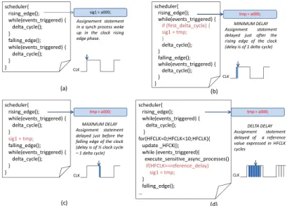
The proposed mutation model aims at implementing signal delays in the TLM IP model. A signal delay is implemented by postponing the actual assignment to the signal (i.e., assignment statement) forward in the simulation time. Since the simulated time of the supported SystemC TLM is cycle-accurate, the granularity of the delays inserted on the signals is defined in delta cycles (finest granularity with abstraction of simulated time) and clock cycles (with accurate simulated time). Given a statement of assignment to a signal (e.g., sig1 = a000 of a synchronous process in Fig. 6(a)), three different mutants are defined to insert a delay on the signal:
1) Minimum delay mutant. The actual assignment to the signal is postponed by one delta cycle. In the example of Fig. 6(b), the statement is delayed jus after the rising edge of the clock.
2) Maximum delay mutant. The actual assignment to the signal is postponed just before the next edge of the clock signal. In the example of Fig. 6(c), the statement is delayed just before the falling edge of the clock.
3) Delta delay mutant. The actual assignment to the signal is postponed exactly of a number of high frequency clock cycles. In the example of Fig. 6(d), the statement is delayed of a number of HFCLK clock cycles equal to reference_delay.
The three mutants are implemented through C++ functions (i.e., saboteur [22]). An instance of the three mutants is injected, in the TLM model of the digital IP, on each signal representing a critical path. The injected mutants are activated, one at a time, to emulate a specific delay on a signal, as explained in the following sections.
1) Verification of digital IPs augmented with Razor sen-sors: The combination of the Minimum and Maximum delay mutants allows the detection and correction features of the Razor sensor (see Section III) to be verified at TLM for the following working time window:
RazorT LM wtw :(CLK rising edge+δ, CLK f alling edge−δ)
Both mutants are necessary to guarantee the sensor ver-ification between the minimum delay (one δ cycle) and the
maximum delay (TCLK
2 ), as explained in Section III-A.
2) Verification of digital IPs augmented with Counter-based sensors: Given a reference delay value for each target signal, the Delta delay mutant is applied to insert a number of clock cycles (HF CLK) of delay on the signal equal to the reference value. The Delta delay mutant allows the detection
scheduler{ rising_edge(); while(events_triggered) { delta_cycle(); } falling_edge(); while(events_triggered) { delta_cycle(); } } sig1 = a000; Assignement statement in a synch process woke up in the clock rising edge phase. scheduler{ rising_edge(); while(events_triggered) { if (first_delta_cycle) { sig1 = tmp; } delta_cycle(); } falling_edge(); while(events_triggered) { delta_cycle(); } } tmp = a000; MINIMUM DELAY Assignment statement delayed just after the rising edge of the clock (delay is of 1 delta cycle)
CLK CLK scheduler{ rising_edge(); while(events_triggered) { delta_cycle(); } sig1 = tmp; falling_edge(); while(events_triggered) { delta_cycle(); } } MAXIMUM DELAY Assignment statement delayed just before the falling edge of the clock (delay is of ½ clock cycle – 1 delta cycle) CLK scheduler{ rising_edge(); while(events_triggered) { delta_cycle(); } for(HFCLK=0;HFCLK<10;HFCLK){ update _HFCK(); while (events_triggered){ execute_sensitive_async_processes() if(HFCLK==reference_delay) sig1 = tmp; } falling_edge(); … DELTA DELAY Assignment statement delayed of a reference value expressed in HFCLK cycles CLK (b) (a) (d) (c) tmp = a000; tmp = a000;
Fig. 6. Mutants defined to insert delays in the TLM model: high-level representation of the TLM scheduling activity of scenario 1 without mutants (a), a minimum delay mutant example (b), a maximum delay example (c), and an example of delta delay mutant applied to the TLM scheduling activity of scenario 2.
feature of the Counter-based sensor to be verified at TLM for the whole observability window (OBS WIN), by preserving the characteristics of maximum resolution (HF CLK period),
maximum error (−THF CLK
2 , +
THF CLK
2 ) and dynamic range
provided by the RTL simulation, as explained in Section III-B. C. Mutation analysis of the augmented digital IPs with the proposed mutants
The abstracted and injected IP and sensors are plugged to an automatic stimuli generator for mutation analysis. The stimuli are generated with the aim of activating the injected mutants and testing the detection and correction mechanism. The outputs are analyzed by comparing the results of the injected model with those generated by a non-injected one. In particular, for the digital IP augmented with the Razor sensor, the output port E of the Razor (see upperside of Fig. 2) is observed in combination with all the output ports of the IP:
• If E = 1, the corresponding mutant has been
ac-tivated and detected (i.e., the statement assignment corresponding to the critical path has been stimulated during simulation). In this case, the correction feature of the Razor (i.e., correction of output values with some clock cycles of delay) can be observed on the output ports of the IP.
• If E = 0 (and the mutant is switched on), either the
mutant has not been activated because the testbench has failed to generate a proper input sequence to stress the mutant (i.e., to reach the assignment statement), or the mutant models a delay outside the range of detection of the sensor. In the first case, the IP outputs of the injected version match with those of the non injected one. In the second case, the IP outputs of the injected vs. non inject versions do not match. For the Counter-based monitor (see lowerside of Fig. 2):
• If M EAS V AL̸= 0, the corresponding mutant has
been activated and detected;
• If M EAS V AL = 0 (and the mutant is switched
on), the testbench has failed to generate a proper input sequence to stress the mutant.
TABLE I. CHARACTERISTICS OF THERTLDIGITALIPAUGMENTED WITH THE SENSORS.
Digital IP RTL PI PO FF Gates Processes
and sensor (loc) (#) (#) (#) (#) Synch. Asynch.
FIR + Razor 1,544 75 80 425 10,698 256 846
FIR + Counter-based 2,532 12 27 462 10,324 41 45
V. EXPERIMENTALRESULTS
The proposed cross-level verification methodology has been applied to a VHDL RTL model of the Finite Impulse Response (FIR) digital filter. Two augmented versions have been generated with the design approach proposed in Section III: FIR+Razor and FIR+Counter-based monitor.
In both versions, a number of sensors (64 Razors, 1 Counter-based) have been inserted to monitor a corresponding number of critical paths of the FIR design. Table I shows the main characteristics of the resulting augmented models. The table reports the number of lines of code of the starting RTL code (Column RTL (loc)), the number of primary input and output pins (Columns PI (#) and PI (#)), the number of flip-flops (Column FF (#)) and area in terms of NAND2 gates after a synthesis with 666 MHz and 45nm technology (Column Gates (#)). Column Processes reports information on the implementation of the FIR functionality, and, in particular, on the number of synchronous and asynchronous processes (see Section IV-A).
The augmented digital IPs have been abstracted to SystemC TLM by using HIFSuite A2T [5]. Table II reports information on the obtained SystemC TLM descriptions in terms of lines of code (column TLM IP (loc)) and SystemC TLM generation time spent by the abstraction tool (TLM gen. time).
The mutants defined in Section IV-B have been injected in the SystemC TLM models. In particular, the Minimum and Maximum delay mutants have been injected in the FIR+Razor model, one for each critical path. The injection phase, which has been made automatic through a SystemC code visitor, required the names of the RTL signals connected to the input D of the Razor sensor (see Fig. 2), for each of the 64 instances of the Razor. Similarly, the FIR+Counter-based monitor has been injected with three mutants (Minimum, Maximum and Delta Delay mutants) for the only critical path analyzed. The mutant injection did not produce a significant increase in the size of the TLM description, as shown in column Injected TLM (loc) of Table II.
The mutation analysis presented in Section IV-C has been finally applied to the obtained TLM models. Inputs stimuli have been randomly generated. The outputs have been an-alyzed by comparing the results of the injected model with those generated by the non-injected one.
As a result of the mutation analysis, all injected mutants have been detected (Column Killed mutants (%)) in both designs. In addition, the FIR+Razor IP has been verified to be able to notify and correct all the injected delays (columns Error risen (%) and Corrected mutants (%), respectively). In the mutation analysis of the FIR+Counter-based, not all detected mutants have been notified as errors. This is due to the fact that the Counter-based monitor compares the detected delay with a tolerance threshold (which has been set in a monitor look-up table). Only mutants resulting in a higher delay have been notified as errors.
These results confirmed the capability of the SystemC TLM models simulated with the proposed methodology in detecting timing delays with a granularity less than the accuracy of the SystemC simulation (i.e., less than a clock cycle). In particular, the Counter-based monitor detected errors up to 13 periods of the high frequency clock and with a tolerance threshold of 8 periods of the high frequency clock. The injected Minimum
TABLE II. EXPERIMENTAL RESULTS OF ABSTRACTION PROCESS,MUTANTS INJECTION AND MUTATION ANALYSIS.
Digital IP RTL sim. TLM IP TLM gen. TLM sim. # injected Injected Injected Killed Corrected Errors Injected Speedup
and sensor (s) (loc) time (s) (s) mutants mutants TLM (loc) mutants mutants risen TLM (s) (x)
FIR + 241.05 32,837 12.58 64.42 128 64 Minimum 33,746 100.00% 100.00% 100.00% 68.19 3.53 Razor 64 Maximum 33,763 100.00% 100.00% 100.00% 67.98 3.55 FIR + 381.68 4,627 2.69 69.86 3 1 Minimum 4,282 100.00% — 0.00% 76.01 5.02
Counter-based 1 Maximum1 Delta 4,2834,282 100.00%100.00% —— 100.00%30.77% 75.8075.89 5.045.03
Delay mutants have not been detected as errors, as they respect the threshold (0% of delays are notified as errors). All the maximum delays have been notified as errors. Finally, delta delays have been equally distributed over the timing interval and notified a 30.77% of delays as errors.
The results show that the proposed mutants effectively reproduce the effect of delays at TLM and that an accurate verification of the monitor correctness is possible at levels of abstractions higher than RTL. All features of the proposed sensors are preserved, from delay identification to delay cor-rection, depending on the starting monitor characteristics.
Finally, Table II reports the execution times of the detection and correction paradigm verified at RTL and TLM, to underline the motivations of this work. Columns RTL sim. (s) and TLM sim. (s) show the simulation time of the digital IP before mutant injection. The RTL to TLM abstraction process reduces the execution time, in average, of 4.5x (3.75x for the Razor monitor and 5.46x for the Counter-based monitor). The injection of mutants slows down the TLM simulation, in average, of 7.1% (Column Injected TLM (s)). However, the obtained speedup between TLM and RTL simulation is, in average, of 3.54x for the verification of the FIR+Razor and 5.03x for the verification of the FIR+Counter-based (column Speedup (x)).
VI. CONCLUSIONS
This paper presented a methodology to verify at system-level (TLM) digital IPs augmented with embedded timing monitors. With the abstraction to TLM, the delay on critical paths is detected since the functionality of the implemented timing monitors is preserved. This allowed to catch at TLM the side-effcts of many physical properties on the performance of digital IPs. The methodology has been applied to the RTL model of a FIR digital filter, which has been augmented with a modified Razor and a Counter-based monitor. The obtained experimental results demonstrate the applicability of the proposed design and verification methodology and the effectiveness of the simulation performance.
REFERENCES
[1] N. Bombieri, D. Drogoudis, G. Gangemi, R. Gillon, E. Macii, M. Pon-cino, S. Rinaudo, F. Stefanni, D. Trachanis, and M. van Helvoort, “SMAC: Smart systems co-design,” in Proc. of Euromicro DSD, 2013, pp. 1–7.
[2] L. Scheffer, L. Lavagno, and G. Martin, EDA for IC System Design, Verification, and Testing. Taylor & Francis, 2010.
[3] M. Vasilevski, F. Pecheux, N. Beilleau, H. Aboushady, and K. Einwich, “Modeling refining heterogeneous systems with systemc-ams: applica-tion to wsn,” in Proc. of ACM/IEEE DATE, 2008.
[4] Carbon Model Studio, http://carbondesignsystems.com/. [5] HIFSuite, http://http://www.hifsuite.com/.
[6] P. Paulin, C. Pilkington, and E. Bensoudane, “Stepnp: a system-level exploration platform for network processors,” IEEE Des. Test. Comput., vol. 19, no. 6, pp. 17–26, 2002.
[7] R. Leveugle, D. Cimonnet, and A. Ammari, “System-level dependability analysis with rt-level fault injection accuracy,” in Proc. of IEEE DFT, 2004, pp. 451–458.
[8] N. Hatami, R. Baranowski, P. Prinetto, and H. Wunderlich, “Efficient system-level aging prediction,” in Proc. of IEEE ETS, 2012, pp. 1–6. [9] S. Borkar, “Designing reliable systems from unreliable components:
the challenges of transistor variability and degradation,” IEEE Micro, vol. 25, no. 6, pp. 10–16, 2005.
[10] O. Unsal, J. Tschanz, K. Bowman, V. De, X. Vera, A. Gonzalez, and O. Ergin, “Impact of parameter variations on circuits and microarchi-tecture,” IEEE Micro, vol. 26, no. 6, pp. 30–39, 2006.
[11] M. Alam, H. Kufluoglu, D. Varghese, and S. Mahapatra, “A compre-hensive model for pmos nbti degradation: Recent progress,” Microelec-tronics Reliability, vol. 47, no. 6, pp. 853 – 862, 2007.
[12] R. Datta, G. Carpenter, K. Nowka, and J. Abraham, “A scheme for on-chip timing characterization,” in Proc. of 24th IEEE VLSI Test Symp., 2006, pp. 24–29.
[13] S. Pei, H. Li, and X. Li, “A high-precision on-chip path delay measure-ment architecture,” IEEE Trans. VLSI Syst., vol. 20, no. 9, pp. 1565– 1577, 2012.
[14] M.-C. Tsai, C.-H. Cheng, and C.-M. Yang, “An all-digital high-precision built-in delay time measurement circuit,” in Proc. of IEEE VTS, 2008, pp. 249–254.
[15] X. Wang, M. Tehranipoor, S. George, D. Tran, and L. Winemberg, “De-sign and analysis of a delay sensor applicable to process/environmental variations and aging measurements,” IEEE Trans. VLSI Syst., vol. 20, no. 8, pp. 1405–1418, 2012.
[16] S. Ghosh, S. Bhunia, A. Raychowdhury, and K. Roy, “A novel delay fault testing methodology using low-overhead built-in delay sensor,” IEEE Trans. Comput.-Aided Design Integr. Circuits Syst., vol. 25, no. 12, pp. 2934–2943, 2006.
[17] K. Bowman, J. Tschanz, N. S. Kim, J. Lee, C. Wilkerson, S. Lu, T. Karnik, and V. De, “Energy-efficient and metastability-immune resilient circuits for dynamic variation tolerance,” IEEE J. Solid-State Circuits, vol. 44, no. 1, pp. 49–63, 2009.
[18] S. Das, D. Roberts, S. Lee, S. Pant, D. Blaauw, T. Austin, K. Flautner, and T. Mudge, “A self-tuning dvs processor using delay-error detection and correction,” IEEE J. Solid-State Circuits, vol. 41, no. 4, pp. 792– 804, 2006.
[19] S. Das, C. Tokunaga, S. Pant, W.-H. Ma, S. Kalaiselvan, K. Lai, D. Bull, and D. Blaauw, “RazorII: In situ error detection and correction for pvt and ser tolerance,” IEEE J. Solid-State Circuits, vol. 44, no. 1, pp. 32– 48, 2009.
[20] T. Sato and Y. Kunitake, “A simple flip-flop circuit for typical-case designs for dfm,” in Proc. of IEEE ISQED, 2007, pp. 539–544. [21] J.-C. Baraza, J. Gracia, S. Blanc, D. Gil, and P.-J. Gil, “Enhancement
of fault injection techniques based on the modification of vhdl code,” IEEE Trans. VLSI Syst., vol. 16, no. 6, pp. 693–706, 2008.
[22] M. Rimen, J. Ohlsson, E. Jenn, J. Arlat, and J. Karlsson, “Fault injection into VHDL models: The MEFISTO tool,” in Proc. of IEEE FTCS, 1994, pp. 66–75.
[23] J. R. Armstrong, F. S. Lam, and P. C. Ward, Test Generation and Fault Simulation for Behavioral Models. Prentice Hall, 1992.
[24] “IEEE Standard SystemC Language Reference Manual,” http:///ieeexplore.ieee.org, 2006.
[25] R. A. DeMillo, R. J. Lipton, and F. G. Sayward, “Hints on test data selection: Help for the practicing programmer,” IEEE Computer, vol. 11, no. 4, pp. 34–41, April 1978.
[26] D. Hyunsook and G. Rothermel, “On the use of mutation faults in empirical assessments of test case prioritization techniques,” IEEE Trans. Softw. Eng., vol. 32, no. 9, pp. 733–752, 2006.
[27] A. Sen and M. S. Abadir, “Coverage metrics for verification of concurrent SystemC designs using mutation testing,” in Proc. of IEEE HLDVT, 2010, pp. 75–81.
[28] H. Le, D. Grosse, and R. Drechsler, “Automatic tlm fault localization for systemc,” IEEE Trans. Comput.-Aided Design Integr. Circuits Syst., vol. 31, no. 8, pp. 1249–1262, 2012.
[29] P. Lisherness and K.-T. Cheng, “SCEMIT: A SystemC error and mutation injection tool,” in Proc. of ACM/IEEE DAC, 2010, pp. 228 –233.
[30] N. Bombieri, F. Fummi, V. Guarnieri, and G. Pravadelli, “Testbench qualification of systemc tlm protocols through mutation analysis,” IEEE Trans. Comput., vol. PP, no. 99, pp. 1–14, 2013.