Scuola Normale Superiore di Pisa
Ph.D. Thesis
Band Structure Engineering
of Ge-rich
SiGe Nanostructures
for Photonics Applications
Giovanni Pizzi
Advisor
Contents
Introduction 1
I Methods 5
1 Adopted models and methods for the electronic states 7
1.1 Crystal geometry of zincblende structures . . . 8
1.2 Tight-binding model . . . 10
1.2.1 Semiempirical approach . . . 13
1.2.2 Spin–orbit coupling . . . 19
1.3 Strain . . . 26
1.3.1 Relation between strains and stresses . . . 30
1.3.2 Strains in mismatched epitaxy and continuum elasticity theory 33 1.3.3 Change of symmetry under biaxial strain . . . 37
1.3.4 Hopping integrals under strain in the TB formalism . . . . 38
1.3.5 Discussion of the parametrizations and diagonal parameters shifts . . . 39
1.3.6 Band structure of Si and Ge under [001] biaxial strain . . . 41
1.3.7 Strain balancing . . . 43
1.4 SiGe alloys and the virtual crystal approximation . . . 44
1.5 Valence band offsets . . . 45
1.6 k ⋅ p model . . . . 47
1.6.1 k ⋅ p model for bulk systems . . . 48
1.6.2 k ⋅ p model for heterostructures: the envelope-function ap-proximation . . . 50
1.7 Effective-mass tensors in the conduction band of Si and Ge . . . 55
1.8 Evaluation of quasi-Fermi energies and effective masses . . . 56
1.8.1 Rotation of the effective-mass tensor . . . 59
1.9 Band bendings and Schr¨odinger–Poisson equation . . . 62
1.10 Evaluation of phonon scattering lifetimes . . . 63
1.11 Interdiffusion due to annealing . . . 65
2 Optical properties of bulk and heterostructured semiconductors 73
2.1 Absorption and gain . . . 73
2.1.1 Calculation of the transition rate W(ω) . . . 75
2.2 Evaluation of the optical properties . . . 78
2.2.1 Optical matrix elements in the tight-binding formalism . . 78
2.2.2 Absorption and gain in the tight-binding model . . . 80
2.2.3 Absorption and gain in the effective-mass approximation . 80 2.3 Spontaneous recombination rate . . . 83
2.3.1 Direct transitions . . . 84
2.3.2 Indirect transitions . . . 86
2.4 2D excitons . . . 93
2.5 Intersubband absorption and oscillator strengths . . . 95
2.5.1 Intersubband absorption . . . 95
2.5.2 Oscillator strengths . . . 97
2.5.3 Absorption coefficient as a function of the oscillator strength 102 2.5.4 Low-temperature limit . . . 103
2.A Appendix: Lineshape function for large broadenings . . . 104
II Applications 107 3 THz emission from Si-compatible multilayer SiGe heterostructures 109 3.1 Introduction . . . 109
3.2 ISB transitions in Ge/SiGe MQWs . . . 113
3.3 Non-radiative lifetimes in Ge/SiGe MQWs . . . 122
3.4 Design of a Ge/SiGe quantum cascade emitter . . . 126
3.4.1 Contacts in the Ge/SiGe quantum cascade structure . . . . 128
3.5 Design of a Si/SiGe quantum cascade emitter . . . 131
3.6 Conclusion of the Chapter . . . 133
3.A Appendix: details of the k ⋅ p multiband code . . . . 135
4 Achieving direct-gap Si/Ge systems 139 4.1 Introduction . . . 139
4.2 Type-I alignment and calculation of the absorption coefficient . . . 140
4.3 Large tensile strain for optical gain in Ge . . . 141
4.4 Small strain and doping . . . 149
4.5 Simulating the photoluminescence . . . 152
4.6 Annealing procedure to increase the tensile strain . . . 157
4.7 Direct-gap Sin/Gemsuperlattices . . . 161
4.8 Conclusion of the Chapter . . . 173
Contents
Appendices 182
A Further addressed topics 185
A.1 SiGe rolled-up nanotubes . . . 186 A.2 Porous silicon . . . 191 A.3 Intersubband polaritons . . . 194
List of publications related to this Thesis 197
Acknowledgements 201
Bibliography 203
List of Figures 223
Introduction
Information and Communication Technology (ICT) is currently dominated by sili-con, because of its advantageous physical and electronic properties, and also due to its large availability. However, the required data transfer rates of modern electronic chips increase very rapidly and are going beyond the switching speeds provided by current state-of-the-art electronics.
Electronic–Photonic Integrated Circuits (EPIC) on Si are probably the most promising answer to this challenge. A laser compatible with the current processing of electronic chips for integrated circuits, based on group-IV materials, is extremely desirable to monolithically integrate electronics and photonics.
Indeed, in the recent years, there has been a renewed interest for Si and Ge as materials for photonics devices [1–3], also thanks to the developments of the their growth technique and to the first demonstration at MIT of a CMOS-compatible optically pumped Ge-on-Si laser [4].
In this Thesis I study bulk and multilayered heterostructures composed of Si, Ge and their alloys with particular attention to Ge-rich systems, with the aim of realizing optical sources in different regions of the electromagnetic spectrum. In particular, the systems investigated are thin layers, superlattices, multiple quantum well (MQW) heterostructures or quantum cascade structures with alternating Si1−xGex layers
of different composition x, coherently grown along the [001] direction on relaxed virtual substrates.
The Thesis is divided in two main Parts. Part I is devoted to the description of the methods that are at the basis of the calculations carried out in the second Part. In particular, in Chap. 1 I describe the models that are used for the evaluation of the electronic states of the studied systems. The two models here adopted are the tight-binding (Sec. 1.2) and the k ⋅ p method (Sec. 1.6). In both cases, the discussion starts from the application of the model to Si or Ge bulk systems, and it is then generalized to the case of multilayer heterostructures. Moreover, I discuss how strain (Sec. 1.3) and alloying (Sec. 1.4) can be taken into account in the calculations, due to the high relevance of these effects in Si/Ge heterostructures. The last Sections of Chap. 1 are devoted to the description of further theoretical models that are adopted in the second Part of the Thesis, such as for instance the solution of the coupled Schr¨odinger– Poisson equations that must be solved to take into account self-consistent charge distribution effects (Sec. 1.9), the evaluation of the intersubband phonon scattering lifetimes (Sec. 1.10), or the simulation of the interdiffusion process due to a thermal
annealing of a MQW system (Sec. 1.11).
Chap. 2 is instead dedicated to the theory of the optical properties of bulk and heterostructured semiconductors. In particular, the general definition of the absorp-tion and gain spectra is presented in Sec. 2.1, and then in Sec. 2.2 I discuss how to calculate these spectra both in the tight-binding framework and in the k ⋅ p effective-mass framework. In Sec. 2.3 the photoluminescence spectra due to the spontaneous recombination in optically-pumped bulk Ge systems is addressed. In Sec. 2.4, 2D excitonic effects on the evaluated absorption spectra are included, and the absorption coefficient in the case of intersubband transitions is addressed in Sec. 2.5.
The models and techniques discussed in Part I are then exploited in Part II which is instead dedicated to several applications, i.e. to the identification and study of different systems that are potential candidates as Si-based light sources.
In particular, this second Part is divided in two Chapters, focusing on two kind of problems which are different both from the point of view of the underlying physics (intersubband vs. interband transitions) and from the point of view of the applications, since the emission frequency is in the far-infrared or in the near-infrared regions, respectively. Consequently, especially for what concerns the applications, the problems addressed in the two Chapters are for many aspects independent. For this reason, a more detailed discussion of the motivations of the investigations of the topics presented in this Thesis can be found in the Introductions of the respective Chapters.
In Chapter 3 I address the use of intersubband transitions in the conduction band of Ge/SiGe MQWs and quantum cascade structures with the final objective of realizing an emitter in the THz region of the electromagnetic spectrum. I start from the study of the absorption due to the intersubband transitions in the conduction band (at the L point) of Ge/SiGe MQW systems (Sec. 3.2). This study is indeed preliminary to the observation of light emission. However, beside the demonstration of intersubband absorption, it is important to study also the non-radiative channels through which the electrons can relax without emission of photons: Sec. 3.3 is devoted to this aim. We then propose a few different designs of THz electroluminescent emitters, based on Ge/SiGe (Sec. 3.4) or on Si/SiGe quantum cascade structures (Sec. 3.5).
In Chapter 4 I focus instead on interband transitions in SiGe systems (thin layers, MQWs and superlattices) with the aim of obtaining a laser emitting in the near-infrared, which could be employed for instance as a source for the optical fiber interconnects used in long-range telecommunications. In particular, in Sec. 4.2 the interband absorption spectrum of a Ge/SiGe MQW system is studied and from comparison with the experimental measures the different involved transitions are identified. In Sec. 4.3 I study the possibility of reaching a direct gap in Ge/SiGe MQW systems by means of a large applied tensile strain, thanks to the different shifts of the conduction Γ and L valleys under biaxial strain. Then, the possibility of reaching positive gain by means of a smaller tensile strain in a strongly n−doped Ge system is analyzed with reference to recent literature results (Sec. 4.4), motivating the development of a code to evaluate the photoluminescence spectrum of bulk-like
Introduction
strained and doped Ge systems; the results obtained with this code are presented and discussed in Sec. 4.5. Furthermore, due to the relevant role of the tensile strain in the relative positioning of the different states in Ge systems, several strategies have been addressed to increase the magnitude of the strain: in particular, in Sec. 4.6 I discuss the effects of thermal annealing on a Ge/SiGe MQW system, focusing on the competitiveness between the redshift of the lowest-energy transitions due to the increase of the biaxial tensile strain, and their blueshift caused by the interdiffusion of the Si atoms in the Ge wells. Eventually, I present a different strategy to obtain a direct-gap structure based on the adoption of short-period Si/Ge superlattices: in Sec. 4.7 I discuss how in this kind of heterostructures the band folding and the reduced symmetry may be able to produce a direct gap, and I then show that in selected superlattices a positive gain can be expected.
Finally, in Appendix A I briefly describe a few further topics that I have addressed: Si/Ge nanotubes, porous silicon and intersubband polaritons. Even if the first two topics are not planar multilayer heterostructures, they show the potential and the peculiar properties of SiGe materials. In the study of the intersubband polaritons, I addressed the specific role of the non-parabolicity of the confined bands and their interactions with cavity modes: the adopted methodology will be further developed for the analysis of intersubband polaritons in SiGe systems.
Part I
Chapter 1
Adopted models and methods for
the electronic states
Many of the electronic and optical properties reported in this Thesis are calculated by means of a first-neighbor tight binding (TB) Hamiltonian with s p3d5s∗orbitals and including spin-orbit interaction. The advantage of this atomistic approach is that it allows us to take into account the geometric details of the whole structure, the chemical composition of the deposited materials and the strain within each layer. The method provides the electronic band structure over the whole Brillouin zone, the spatial and orbital compositions of the states, and the matrix elements of optical transitions. Moreover, the tight binding model is most appropriate for large scale electronic structure calculations, especially when implemented with O(N) strategies (see e.g. Ref. [5] and references therein, and Refs. [6, 7]).
However, there are cases (that will be described in detail in the following Chap-ters) when simpler but faster methods are more appropriate. In particular, we will describe and adopt for some selected applications a multiband k ⋅ p effective-mass model. The disadvantage of this model is that it is not as numerically accurate as the tight binding (see e.g. Refs. [8–11]). However, it has mainly two advantages. The first is that it significantly reduces the computation time. This is a strong requirement in the process of optimization of the design of complicated structures (see e.g. Secs. 3.4, 3.5 and 3.A): for such an application, the calculation has to be as real-time as possible, because we need to change many times the input parameters in order to obtain the best design. In practice, each run can last in the worst case tens of seconds, but not hours. The second advantage is that the k ⋅ p model can give a more intuitive descrip-tion of many of the physical properties of the system, often allowing to understand their qualitative behavior or even providing for them analytic expressions.
In this Chapter, we describe both models for the calculation of the electronic properties of bulk and heterostructured semiconductors, with special attention to the case of Si and Ge. Furthermore, we also address some further theoretical models that will be adopted in the second Part of the Thesis.
Table 1.1 – Lattice constants of some semiconductors which crystallize in the diamond
structure, taken from Wyckoff [12].
Crystal a( ˚A) C Diamond 3.566 79 (20○C) Si Silicon 5.430 70 (25○C) 5.445 (1300○C) Ge Germanium 5.657 35 (20○C) 5.656 95 (18○C) α−Sn Tin (gray) 6.4912 a y z x τ1 τ3 τ2
Figure 1.1 – FCC lattice. The primitive
vec-tors are τ1 = a/2(0, 1, 1), τ2 = a/2(1, 0, 1) and τ
3= a/2(1, 1, 0), where a is the side of the
con-ventional unit cell. The primitive cell is shown with a darker color.
The conventional unit cell, having a basis of four atoms in the positions d1= (0, 0, 0), τ1, τ2and τ
3, emphasizes the full cubic symmetry Ohof
the lattice.
1.1
Crystal geometry of zincblende structures
This Thesis is focused on silicon (Si) and germanium (Ge), which are group IV semiconductors and crystallize in the diamond structure. Since this structure is a special case of the zincblende structure, typical of most group III-V semiconductors, like gallium arsenide (GaAs), indium arsenide (InAs), etc., in this Section we describe the more general zincblende structure.
The Bravais lattice of the zincblende structure is face centered cubic (FCC) with a basis of two atoms, so that it can be seen as two interpenetrating FCC lattices. We can choose the three translation vectors of the FCC lattice as
τ
1=a/2(0, 1, 1), τ2=a/2(1, 0, 1), τ3=a/2(1, 1, 0), (1.1)
as represented in Fig. 1.1; the primitive cell formed by these vectors has volume a3/4. However, in order to emphasize the full cubic symmetry of the Bravais lattice, one often uses the larger conventional unit cell with side a, also shown in Fig. 1.1. The values of a (the lattice constant) for some common semiconductors which crystallize in the diamond structure are given in Table 1.1.
As already mentioned, the zincblende structure has two atoms in the primitive cell, one in the origin d1= (0, 0, 0), and one at one fourth of the diagonal of the cube:
1.1 Crystal geometry of zincblende structures
a
Figure 1.2 – Conventional unit cell of the zincblende structure. First-neighbor bonds are
also shown. In this structure, one kind of atoms (e.g. the anions, red in the Figure) form a FCC lattice. The other kind of atoms (cations, blue in the Figure) also form a FCC lattice, which is displaced by one fourth of the diagonal of the conventional unit cell with respect to the FCC lattice of the anions. If the two atoms are equal, one recovers the diamond structure. If we use the primitive cell with translation vectors given in Eq. (1.1) (see also Fig. 1.1), there are only two atoms in the primitive cell: the anion, lying at d1 = (0, 0, 0), and the cation,
lying at d2=a/4(1, 1, 1).
In the zincblende structure, each atom has four first neighbors of opposite kind, which form a regular tetrahedron centered on the atom. One of such tetrahedrons is shown in blue in the Figure.
possible to notice that each atom lies at the center of a regular tetrahedron formed by its four first neighbors. We emphasize here that the knowledge of the position of the first neighbors is of great importance for the application of the tight-binding model. We thus write explicitly the coordinates of the positions of the four first neighbors with respect to the reference atom. In the case of the atom centered on the origin, the four nearest-neighbor positions are
d2=a1= (1/2,1/2,1/2), d2− τ1=a2= (1/2, −1/2, −1/2),
d2− τ2=a3= (−1/2,1/2, −1/2), d2− τ3 =a4= (−1/2, −1/2,1/2), (1.2) while for the atom centered on d2the relative positions are
−a1= (−1/2, −1/2, −1/2), −a2= (−1/2,1/2,1/2), −a3= (1/2, −1/2,1/2), −a4= (1/2,1/2, −1/2).
The two atoms in d1and d2are different in the case of group III-V materials
(for instance, in the case of GaAs, we have an arsenic atom in the origin and a gallium atom in d2), and in this case we designate them as the anion and the cation,
Γ X L W K U kx ky kz
Figure 1.3 – Brillouin zone of a crystal with a FCC
Bra-vais lattice. The reciprocal lattice is a body-centered cubic (BCC) and the Brillouin zone is a truncated oc-tahedron, centered on Γ.
The points of high symmetry are also shown.
respectively. For the diamond structure, the two atoms in the primitive cell are instead equal.
The corresponding primitive vectors of the FCC reciprocal lattice are
g1= 2π a (−1, 1, 1), g2= 2π a (1, −1, 1), g3= 2π a (1, 1, −1),
which form a BCC lattice. The Brillouin zone is the well known truncated octahedron, depicted in Fig. 1.3. Some points of high symmetry in the Brillouin zone are denoted by conventional names: Γ = (0, 0, 0), X = 2aπ(1, 0, 0), L = 2 π a ( 1 2, 1 2, 1 2 ), W = 2π a (1, 1 2, 0) , K = 2π a ( 3 4, 3 4, 0) , U = 2π a (1, 1 4, 1 4 ).
1.2
Tight-binding model
One of the models that we use in this work in order to study the electronic and optical properties of Si–Ge nanostructures is the tight-binding model (TB).
When the atoms are brought together to form the crystal, their orbitals overlap and the energy levels spread leading to the formation of bands, i.e. the actual levels in the solid.
We denote by rnνthe position of a generic atom of the crystal, where n indicates the cell to which the atom belongs and ν indexes the different atoms within the cell; in particular, rnνcan be written as rnν= τn+dν, where τnis a translation vector of the FCC Bravais lattice and dνis the position of the atom ν within the cell.
The Hamiltonian of an isolated atom of type ν centered on rnνis hν(r − rnν)and the corresponding Schr¨odinger equation is given by
hνϕνm(r − rnν) = [ p2
2m
+V(a)(r − rνm)]ϕνm(r − rnν) = ˜Eνmϕνm(r − rnν), (1.3) where m indexes the states and V(a)is the atomic potential acting on the electron, due to the nucleus and the other electrons. We know that we can choose solutions
1.2 Tight-binding model
with a definite angular symmetry (for example, if the Hamiltonian depends only on the magnitude of r and not on its angular part, we can separate the orbitals ϕνmin a radial and an angular part, and choose the angular part as a linear combination of spherical harmonics, so that the orbitals have symmetry s, px, py, pzand so on).
We always assume, moreover, that the atomic orbitals ϕνm(r − rnν)are L¨owdin orbitals, i.e., different orbitals are orthogonal to each other. For orbitals centered on the same atom this is obvious, as we can always choose an orthonormal set of eigenfunctions for the problem (1.3). For atoms centered on different sites, we can first obtain a set of non-orthogonal orbitals simply solving Eq. (1.3). With a procedure shown in Ref. [13] we can at this point change the basis set to obtain the L¨owdin orbitals with the requested property
⟨ϕνm(r − rnν) ∣ϕν′m′(r − rn′ν′)⟩ =δmm′δnn′δνν′. (1.4)
The simple orthogonalization algorithm presented in [14] has moreover the advantage that the L¨owdin orbitals ϕνm show the same symmetry properties as the original atomic orbitals, so that we can still speak of orbitals of s-symmetry, px-symmetry, and so on. This information is contained in the index m of ϕνm.
When we consider the full Hamiltonian of the crystal, the actual wavefunctions must satisfy the Bloch theorem because of the discrete translational symmetry of the lattice; we can write them in the form of Bloch sums
Φνm(k, r) = √1 N∑n
eik⋅rnνϕ
νm(r − rnν) (1.5)
where N is the number of primitive cells in the crystal and the sum over n runs over all the N cells. Note that these Bloch sums are orthonormal because of Eq. (1.4).
We assume that the single-particle Hamiltonian H for an electron of the crystal can be written in the form
H = p
2
2m
+V(r),
where V (the crystalline potential) is assumed to be the sum of the atomic potentials V(a):
V(r) = ∑
n,ν
V(a)(r − rnν). (1.6)
The eigenfunctions of the total Hamiltonian H with given k vector can be written as linear combinations of the orthonormal Bloch sums Φνm(k, r)
Ψk(r) = ∑
ν,m
CνmΦνm(k, r)
and the coefficients Cνmcan be obtained by simply diagonalizing the Hamiltonian matrix Hνm,ν′m′(k), whose matrix elements are
Hν′m′
,νm(k) = ⟨Φν′m′(k, r)∣H∣Φνm(k, r)⟩ .
Let us explicitly compute the matrix elements Hν′m′
We can split V , given in Eq. (1.6), in two parts, separating the contribution of the atom in dν′: H = p 2 2m +V(r) = p 2 2m +V(a)(r − dν′) +V′(r) = hν′+V′
where V′(r) contains all the remaining terms of the potential, i.e. the atomic poten-tials centered on sites different from dν′.
Using now the fact that ϕνmis eigenfunction of the atomic Hamiltonian hν, as stated in Eq. (1.3), and the explicit expression for the orthonormal Φνmfunctions, given in Eq. (1.5), we obtain
Hν′m′ ,νm(k) = ⟨Φν′m′(k, r)∣H∣Φνm(k, r)⟩ = Eν′m′δνν′δmm′+ + ∑ τn eik⋅(τn+dν−dν′) ∫ dr ϕ∗ν′m′(r − dν′)V′(r)ϕνm(r − τn−dν). (1.7)
The sum of the previous expression is over all translation vectors τnsuch that ν and ν′belong to different sites. Note that the energy Eν′m′contains the atomic eigenvalue
˜
Eν′m′ of the atom in dν′corrected by the crystal field contribution, which originates
from the term in Eq. (1.7) with τn =0 and ν = ν′. This term is of the form
∫ dr ϕ∗ν′m′(r − dν′)V′(r)ϕν′m′(r − dν′), (1.8) where we stress again that V′is the sum of all contributions to the potential coming from atoms other than the one sitting at dν′, and both orbitals are centered on the
same position dν′. As a consequence, Eν′m′ feels its environment, i.e. it contains
contributions due to the symmetry of the crystal structure in which the atom is embedded.
As already said, to get the energy levels we only need to solve the eigenvalue problem
HΨ(k) = E(k)Ψ(k), i.e. diagonalize the Hamiltonian matrix Hν′m′
,νm(k). This is, however, not simple at
all.
The first difficulty that we encounter is in the evaluation of the last term of Eq. (1.7). This term rises two problems: first of all we have to work with the sum over
τn that, even if not infinite, is composed of an unmanageable large number of terms.
However, we can make a first approximation considering only those orbitals centered on atoms that are not too far apart, because we are assuming that the orbitals of interest are quite localized and do not interact significantly if they are spatially well separated. We can then adopt the first-neighbor approximation, where we sum only on the nearest-neighbor atoms (in the case of the zincblende structure, only on four atoms), second-neighbor approximation and so on. A further approximation is the so called two-center approximation. Indeed, expanding V′(r) using Eq. (1.6), we see that in general we have integrals in Eq. (1.7) where the two wavefunctions are centered on two different atoms, and interact through an atomic potential centered
1.2 Tight-binding model
on a third site. Always assuming well localized orbitals, we can neglect all those contributions where the three sites are different, and consider only the terms of the following form:
⟨ϕν′m′(r − dν′) ∣V(a)(r − dν− τn) ∣ϕνm(r − dν− τn)⟩. (1.9) The second problem that we have to face with, is that we have an infinite number of L¨owdin orbitals on each site, and therefore also the Hamiltonian matrix is infinite. To obtain a finite matrix, allowing us to diagonalize it with standard methods, we consider only a finite set of orbitals, in particular those of the outermost atomic shells. This choice is physically motivated by the fact that the inner orbitals are quite ineffective to provide relevant features in the electronic properties of the crystal, being tightly bound to the nuclei. If a calculation is performed taking into account also these orbitals, we would get that they generate dispersionless (k−independent) core bands, that correspond to an infinite electronic effective mass. Moreover, these (completely filled) bands are deep well below the chemical potential level, and therefore also an excitation of an electron to a higher band is impossible using photons in the visible range or with lower frequency.
The topmost occupied valence bands show on the contrary a complicated disper-sion relation E(k); moreover there is the actual possibility that some electrons are transferred to the empty conduction bands, originating interesting transport and optical properties of the semiconductor.
The simplest choice of orbitals that produces reasonable results is the so called sp3
tight-binding model, where we consider only one orbital with s symmetry and three p orbitals (px, pyand pz) centered on each atom of the primitive cell, reducing the total number of orbitals to eight in the case of the zincblende structure. In this way we have to diagonalize only a 8 × 8 matrix, simplifying notably the computation. This description, however, is quite poor, and indeed it lacks some of the most important features of the band dispersion of the group IV and III-V semiconductors. In the literature, there have been different attempts to solve this problem, typically increasing the order of neighbors which are taken into account in the calculation, or introducing additional orbitals for each atom. With this second method, at the expense of an increase of the dimension of the Hamiltonian matrix, one obtains a great improvement of the results of the computation, allowing for the description of some features that were missed by the simple s p3model.
The model that is used throughout this work is the s p3d5s∗model in the first-neighbor approximation, that we now describe in detail.
1.2.1 Semiempirical approach
An upgrade of the minimal s p3basis set model has been obtained introducing, for each atom in the primitive cell, an unoccupied excited s-type orbital [15]; this gives a better description of the conduction bands of the semiconductors. Such orbitals are denoted by s∗to distinguish them from the other lower-energy s orbitals.
The major improvement in the description of the conduction bands, however, is obtained by the introduction of d-type orbitals, as explained in Jancu et al. [16]. One of the main achievements of such a choice is a better agreement with the known sequence of the energy levels, and a better reproduction of the transverse effective masses for the conduction band minima at the L point and along the Γ−X line in the Brillouin zone.
Throughout this work, we thus adopt ten atomic-like orbitals for each atom, denoted by their symmetry as
s; x, y, z ´¹¹¸¹¹¹¶ p ; x y, xz, yz, x2−y2, 3z2−r2 ´¹¹¹¹¹¹¹¹¹¹¹¹¹¹¹¹¹¹¹¹¹¹¹¹¹¹¹¹¹¹¹¹¹¹¹¹¹¹¹¹¹¹¹¹¹¹¹¹¹¹¹¹¹¹¹¹¹¹¹¹¹¹¹¹¹¹¹¹¹¹¹¹¹¹¹¹¹¸¹¹¹¹¹¹¹¹¹¹¹¹¹¹¹¹¹¹¹¹¹¹¹¹¹¹¹¹¹¹¹¹¹¹¹¹¹¹¹¹¹¹¹¹¹¹¹¹¹¹¹¹¹¹¹¹¹¹¹¹¹¹¹¹¹¹¹¹¹¹¹¹¹¹¹¹¹¹¶ d ; s∗. (1.10)
To distinguish between orbitals belonging to different atoms, we use a specific site label. For zincblende structures, e.g., we denote with sathe s orbital centered on the anion, and with scthe orbital centered on the cation, and similarly for the other orbitals. We will use this notation also for group IV semiconductors if we need to distinguish between the two atoms in the basis, even if the two atoms are of the same kind.
As already said, we limit ourselves to interactions between first neighbors and consider only two-center integrals. The generic integral that we must compute in order to obtain the matrix elements given by Eq. (1.7) is therefore of the form
⟨ϕν′m′(r − dν′) ∣V(a)(r − dν− τn) ∣ϕνm(r − dν− τn)⟩. (1.11)
In the semiempirical approach these integrals, as well as the energies Eνmof Eq. (1.7), are taken as parameters, and are obtained by fitting specific features of the band dispersion of the bulk semiconductor under study. Typically, such features are the values of the energy bands at high-symmetry points of the Brillouin zone and the effective masses, which are obtained from experimental data or from other theoretical methods. The empirical tight-binding model, in this sense, can be seen as an interpolation method that gives the energy bands for all points in the Brillouin zone, starting from a limited set of energies. This semiempirical approach to the tight-binding method was first introduced by Slater and Koster [14].
Using this approach we want now to show that, for a s p3d5s∗model with interac-tions limited to first neighbors, we need only a small set of independent two-center integrals to obtain the full band dispersion. These are denoted (for group IV crystals) by V(ssσ), V(spσ), V(ppσ), V(ppπ), V(sdσ), V(pdσ), V(pdπ), V(ddσ), V(ddπ), V(ddδ), V(s∗sσ), V(s∗s∗σ), V(s∗pσ), V(s∗dσ). (1.12)
What we mean is that all integrals of the form of Eq. (1.11) can be expressed by appropriate linear combinations of the independent integrals (1.12), where the
1.2 Tight-binding model
coefficients depend on the director cosines of the vector R = dν+ τn−dν′ that joins
the two atoms at dν′and at τn+dν.
To clarify this concept, we now discuss the meaning of the integrals (1.12). In the case of two s orbitals, the angular momentum quantized in the direction of the vector joining the two atoms can only be zero. However, if we consider two p orbitals (see Fig. 1.4), we can overlap them along the direction of the orbital; in this case we speak of a σ bond, and the angular momentum along the axis is still zero. We can however let them overlap in a direction orthogonal to the orbitals, e.g. considering the interaction between two pxorbitals, but with the two atoms aligned along the z direction: this type of bond is called a π bond, and now the angular momentum along z is ħ.
In particular, if the vector R joining the two atoms is along the z direction, we can define the two-center integrals introduced in (1.12) by
⟨s∣H∣s⟩ = V(ssσ); ⟨s∣H∣pz⟩ =V(spσ);
⟨pz∣H∣pz⟩ =V(ppσ); ⟨px∣H∣px⟩ = ⟨py∣H ∣ py⟩ =V(ppπ). Moreover, we have that
⟨s∣H∣px⟩ = ⟨s∣H∣py⟩ =V(spπ) = 0 (1.13) because, if the Hamiltonian includes only the two interacting atoms, then it has a cylindrical symmetry along the axis R = dν+ τn−dν′joining the two atoms. If we
consider that the angular part of the orbitals is simply a spherical harmonic function Ylm, with azimuthal direction R, then we see that the matrix element (1.13) of the Hamiltonian vanishes because the two spherical harmonics of the orbitals at the two centers have different m.
In the crystal, however, the direction of the vectors R joining two atoms are in general neither parallel nor orthogonal to the directions of the axes x, y, z that we have chosen to define the p orbitals; to get the interaction parameter for a generic direction, we have to expand the spherical harmonics which define the angular part of our orbitals along the direction of R. The matrix element is therefore a linear combination of the integrals of (1.12). A graphical representation of one possible case is given in Fig. 1.4.
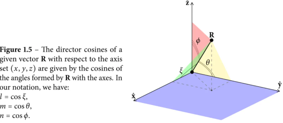
A complete table of all matrix elements needed for a s p3d5s∗basis is reported in Table 1.2, where l , m, and n denote the director cosines of R with respect of the x, y, z axes, as shown in Fig. 1.5. These matrix elements are known as the Slater–Koster parameters.
For the sake of completeness, we mention that in the case of group III-V semi-conductors, the only difference is that we have to distinguish for instance between V(sapcσ) and V(scpaσ): we have indeed different energies depending on whether
the s orbital is centered on the anion or on the cation. The number of independent integrals will be slightly larger, but except for this there is no conceptual difference from what we have presented up to now for group IV semiconductors.
Table 1.2– Slater–Koster parameters up to d−type orbitals in terms of two-center integrals. In this table, we have denoted simply with (ssσ ) the independent integral Vssσ, with (pdπ) the integral Vpd πand so on.
Es,s (ssσ) Es,x l(spσ) Ex ,x l2(ppσ) + (1 − l2)(ppπ) Ex , y lm(ppσ) − lm(ppπ) Ex ,z ln(ppσ) − ln(ppπ) Es,x y √ 3l m(sdσ ) Es,x2−y2 1 2 √ 3(l2−m2)(sdσ) Es,3z2−r2 [n2−1 2(l 2+m2)](sdσ) Ex ,x y √ 3l2m(pdσ) + m(1 − 2l2)(pdπ) Ex , yz √3l mn(pdσ ) − 2l mn(pdπ) Ex ,zx √3l2n(pdσ) + n(1 − 2l2)(pdπ) Ex ,x2−y2 1 2 √ 3l (l2−m2)(pdσ) + l(1 − l2+m2)(pdπ) Ey,x2−y2 1 2 √ 3m(l2−m2)(pdσ) − m(1 + l2−m2)(pdπ) Ez,x2−y2 1 2 √ 3n(l2−m2)(pdσ) − n(l2−m2)(pdπ) Ex ,3z2−r2 l[n2− 1 2(l 2+m2)](pdσ) −√3l n2(pdπ) Ey,3z2−r2 m[n2− 1 2(l 2+m2)](pdσ) −√3mn2(pdπ) Ez,3z2−r2 n[n2− 1 2(l 2+m2)](pdσ) +√3n(l2+m2)(pdπ) Ex y,x y 3l2m2(ddσ) + (l2+m2−4l2m2)(ddπ) + (n2+l2m2)(ddδ) Ex y, yz 3l m2n(ddσ) + ln(1 − 4m2)(ddπ) + ln(m2−1)(ddδ) Ex y,zx 3l2mn(ddσ) + mn(1 − 4l2)(ddπ) + mn(l2−1)(ddδ) Ex y,x2−y2 3 2lm(l 2−m2)(ddσ) + 2lm(m2−l2)(ddπ) +1 2lm(l 2−m2)(ddδ) Eyz,x2−y2 3 2mn(l 2−m2)(ddσ) − mn[1 + 2(l2−m2)](ddπ)+ mn[1 +1 2(l 2−m2)](ddδ) Ezx ,x2−y2 3 2nl(l 2−m2)(ddσ) + nl[1 − 2(l2−m2)](ddπ)− nl[1 −1 2(l 2−m2)](ddδ) Ex y,3z2−r2 √ 3l m[n2− 1 2(l 2+m2)](ddσ) − 2√3l mn2(ddπ)+ 1 2 √ 3l m(1 + n2)(ddδ) Eyz,3z2−r2 √ 3mn[n2− 1 2(l 2+m2)](ddσ) +√ 3mn(l2+m2−n2)(ddπ)− 1 2 √ 3mn(l2+m2)(ddδ) Ezx ,3z2−r2 √ 3l n[n2− 1 2(l 2+m2)](ddσ) +√ 3l n(l2+m2−n2)(ddπ)− 1 2 √ 3l n(l2+m2)(ddδ) Ex2−y2,x2−y2 3 4(l 2−m2)2(ddσ) + [l2+m2− (l2−m2)2](ddπ)+ [n2+ 1 4(l 2−m2)2](ddδ) Ex2−y2,3z2−r2 1 2 √ 3(l2−m2)[n2− 1 2(l 2+m2)](ddσ)+ √ 3n2(m2−l2)(ddπ) + 1 4 √ 3(1 + n2)(l2−m2)(ddδ) E3z2−r2,3z2−r2 [n2−1 2(l 2+m2)]2(ddσ) + 3n2(l2+m2)(ddπ)+ 3 4(l 2+m2)2(ddδ)
1.2 Tight-binding model x y θ Ex,x
=
= x y θ cos2(θ )V ( p pσ )+
+ x y θ sin2(θ )V ( p pπ)Figure 1.4 – Graphical example of the interaction between orbitals on different sites. In
this case, the interaction between two pxorbitals is shown and is decomposed into its two contributions V (ppσ ) and V (ppπ).
Figure 1.5 – The director cosines of a
given vector R with respect to the axis set (x, y, z) are given by the cosines of the angles formed by R with the axes. In our notation, we have:
l = cos ξ, m = cos θ, n = cos ϕ. ξ θ ϕ R ˆx ˆy ˆz
We can now apply these results in our specific case. For the zincblende structure, the director cosines of the vectors joining an anion at d1=0 to its four first neighbors
are (see the relations (1.2)):
l m n d2 √1 3 1 √ 3 1 √ 3 d2− τ1 √13 −√13 −√13 d2− τ2 −√1 3 1 √ 3 − 1 √ 3 d2− τ3 −√13 −√13 √13 (1.14)
while for a cation at d2the four vectors are −d2, −(d2− τ1), −(d2− τ2), −(d2− τ3),
i.e. the opposites of the vectors for an anion. We note here that we are assuming that the atom sitting in the origin is an anion; however, this is only a convention and we could choose to put instead the cation in the origin. The results are the same, because we can go from one description to the other by simply translating the origin of d2
and performing an inversion of the axes. Using this transformation, the anions take the place of the cations and vice versa.
Using these coefficients, we can express all integrals needed to obtain the Hamil-tonian matrix as a function of the Slater–Koster parameters reported in Table 1.2, so that a generic interaction term between an orbital i of the anion a, sitting in the origin, and an orbital j of the cation c, is of the form
Hi jac(k) = ∑ first neighbors eik⋅(τn+d2)⟨ϕa i(r)∣H∣ϕcj(r − d2− τn)⟩ = = ∑ n=0,1,2,3 eik⋅(d2−τn)Ei j( d2− τn), (1.15)
where we have defined τ0= (0, 0, 0) and Ei jis a Slater–Koster parameter.
We notice, now, that all the integrals between the center atom and the four first neighbors have the same absolute value, and differ only in a sign. We can therefore rewrite Eq. (1.15) as
Haci j(k) = Ei j(d2) ∑
n=0,1,2,3
eik⋅(τn+d2)
sign(n),
where sign(n) represents the relative sign of the integral for the atom in position
d2− τnand that for the atom in position d2.
Considering all the possibilities for the relative signs, we obtain that the sum of the exponentials can assume only four different values, called phase factors1:
g0=4(cos x cos y cos z − i sin x sin y sin z), (1.16a) g1=4(− cos x sin y sin z + i sin x cos y cos z), (1.16b) g2=4(− sin x cos y sin z + i cos x sin y cos z), (1.16c) g3=4(− sin x sin y cos z + i cos x cos y sin z), (1.16d)
where we have defined x = akx 4 , y = aky 4 , z = akz 4 .
Using the above definitions, we can now write the 20 × 20 Hamiltonian matrix for a zincblende crystal with two atoms in the primitive cell, in the s p3d5s∗basis, as follows:
Hi j= (
Haa Hac
Hca Hcc ), (1.17)
1
The four phase factors are obtained in the following cases:
g0∶ sign(0) = sign(1) = sign(2) = sign(3) = 1,
g1∶ sign(0) = sign(1) = 1, sign(2) = sign(3) = −1,
g2∶ sign(0) = sign(2) = 1, sign(1) = sign(3) = −1,
1.2 Tight-binding model
where Haa, Hac, Hcaand Hccare 10 × 10 matrices.
In particular, Haa is the diagonal matrix composed of the atomic eigenvalues corrected by the crystal field contribution; its elements are
Esa, Eap, Eap, Eap, Ead, Eda, Ead, Eda, Ead, Esa∗
and analogously Hccfor the cation.
We have also that Hca = (Hac)†, because the Hamiltonian is Hermitian. The block Haccontains the interactions between the anion and the cation. Its explicit form is shown in Table 1.3.
Diagonalizing the matrix Hi j(k) of Eq. (1.17) we obtain twenty (real) eigenvalues, which are the allowed energies for the electron.
If we plot these energies versus the k vector, we obtain the bands of the crystal; an example for silicon is reported in Fig. 1.6, where we have also shown the path followed in k space.
1.2.2 Spin–orbit coupling
For a more precise analysis of the electronic states, also relativistic effects should be included. Indeed this contribution, even if often negligible on the conduction bands, produces instead quite important effects especially at the top of the valence bands (which are mainly composed of p-type states). The correction due to relativistic effects is more important for heavy elements. For most semiconductors, however, these effects are small and we can limit to first-order perturbation theory: for instance, the separation at Γ of the topmost valence bands is only 0.04 eV for silicon (Z = 14) and 0.29 eV for germanium (Z = 32).
To include these effects, we start from the Dirac relativistic equation [cα ⋅ p + βmc2+V(r)]ψ = Wψ.
Here ψ is a four-component spinor, p is the momentum operator −iħ∇, W = E + mc2 is the total energy (including the rest energy mc2) and α and β are given by
α = (0 σ
σ 0), β = (1 0 0 −1
), where 1 is the 2 × 2 unit matrix and σ are the usual Pauli matrices
σx= (0 1 1 0), σy= ( 0 −i i 0), σz= (1 0 0 −1 ). (1.18)
Using the Foldy–Wouthuysen transformation [17], we can decouple the strong and weak components of the Dirac spinor. If we consider only the first terms of an expansion in the ratio p/mc, we obtain the following equation for the upper two-component spinor: [p 2 2m +V(r) − p 4 8m3c2− ħ2 4m2c2∇V ⋅ ∇ + ħ 4m2c2σ ⋅ (∇V × p)] ψ = Eψ.
T a b le 1.3 –H a c m at rix w hic h des cr ib es th e in terac tio n b et w een an anio n in th e o rig in an d a ca tio n in d 2. W e h av e den o te d sim p ly w it hx 2 th ex 2 − y 2 d − typ e o rb ita l. If w e ar e de a lin g w ith a g ro u p III-V semico n d uc to r, th e elem en ts den o te d w it h a tilde ar e to b e defin ed w ith th e fir st o rb ita l cen ter ed o n a ca tio n an d th e se co n d o n an anio n, i.e . w e h av e to u se , fo r in st an ce ,V ( s cp aσ ) in st ead o fV ( s ap cσ ) (f o r th os e w it h o u t tilde , th e fir st cen ter is in st ead o n an anio n). Th e o rder o f th e b a si s is th at rep o rt ed in E q . (1.1 0), i.e .s ,p x ,p y ,p z ,d x y ,d x z ,d yz ,d x 2 −y 2 ,d 3z 2 −r 2 ,s ∗ fo r e ac h at o m in th e p rimi tiv e ce ll. ⎛ ⎜ ⎜ ⎜ ⎜ ⎜ ⎜ ⎜ ⎜ ⎜ ⎜ ⎜ ⎜ ⎜ ⎜ ⎜ ⎜ ⎜ ⎜ ⎜ ⎜ ⎜ ⎜ ⎜ ⎜ ⎜ ⎜ ⎜ ⎜ ⎜ ⎜ ⎜ ⎜ ⎜ ⎜ ⎝ g 0E s ,s g 1E s ,x g 2E s ,x g 3E s ,x g 3E s ,x y g 2E s ,x y g 1E s ,x y 0 0 g 0E s ,s ∗ −g 1 ˜E s , x g 0E x ,x g 3E x , y g 2E x , y g 2E x ,x y g 3E x ,x y g 0E x , yz g 1E x ,x 2 − g 1 √ 3 E x ,x 2 −g 1 ˜E s ∗ ,x −g 2 ˜E s ,x g 3E x ,y g 0E x , x g 1E x , y g 1E x ,x y g 0E x , yz g 3E x ,x y −g 2E x , x 2 − g 2 √ 3 E x ,x 2 −g 2 ˜E s ∗ , x −g 3 ˜E s ,x g 2E x ,y g 1E x ,y g 0E x ,x g 0E x , yz g 1E x ,x y g 2E x , x y 0 2 g 3 √ 3 E x ,x 2 −g 3 ˜E s ∗ , x g 3 ˜E s ,x y −g 2 ˜E x ,x y −g 1 ˜E x ,x y −g 0 ˜E x , yz g 0E x y , x y g 1E x y , xz g 2E x y , xz 0 − 2 g 3 √ 3 E xz ,x 2 g 3 ˜E s ∗ ,x y g 2 ˜E s ,x y −g 3 ˜E x ,x y −g 0 ˜E x , yz −g 1 ˜E x ,x y g 1E x y , xz g 0E x y ,x y g 3E x y , xz g 2E xz ,x 2 g 2 √ 3 E xz ,x 2 g 2 ˜E s ∗ ,x y g 1 ˜E s ,x y −g 0 ˜E x , yz −g 3 ˜E x ,x y −g 2 ˜E x ,x y g 2E x y , xz g 3E x y , xz g 0E x y ,x y −g 1E xz , x 2 g 1 √ 3 E xz ,x 2 g 1 ˜E s ∗ ,x y 0 −g 1 ˜E x ,x 2 g 2 ˜E x ,x 2 0 0 g 2E xz ,x 2 −g 1E xz ,x 2 g 0E x 2 ,x 2 0 0 0 g 1 √ 3 ˜E x ,x 2 g 2 √ 3 ˜E x , x 2 − 2 g 3 √ 3 ˜E x ,x 2 − 2 g 3 √ 3 E xz ,x 2 g 2 √ 3 E xz , x 2 g 1 √ 3 E xz ,x 2 0 g 0E x 2 ,x 2 0 g 0 ˜E s ,s ∗ g 1E s ∗ ,x g 2E s ∗ ,x g 3E s∗ ,x g 3E s ∗ ,x y g 2E s ∗ ,x y g 1E s∗ ,x y 0 0 g 0E s ∗ ,s ∗ ⎞ ⎟ ⎟ ⎟ ⎟ ⎟ ⎟ ⎟ ⎟ ⎟ ⎟ ⎟ ⎟ ⎟ ⎟ ⎟ ⎟ ⎟ ⎟ ⎟ ⎟ ⎟ ⎟ ⎟ ⎟ ⎟ ⎟ ⎟ ⎟ ⎟ ⎟ ⎟ ⎟ ⎟ ⎟ ⎠
1.2 Tight-binding model L L Γ Γ X X W W K K L L W W X X U=K U=K Γ Γ -10 0 10 20 30 Energy (eV)
Silicon (without spin-orbit)
Γ Γ X L W K U≡K Γ Γ X L W K U≡K
Figure 1.6 – Band structure of silicon (without the introduction of spin–orbit interactions),
using the parametrization of Jancu et al. [16]. The path followed in k space is also shown (it is split in two parts only for graphical reasons).
The first two terms on the left-hand side are the non-relativistic Hamiltonian. The three following terms
Hv= − p 4 8m3c2, Hd = − ħ2 4m2c2 ∇V ⋅ ∇, Hso= ħ 4m2c2σ ⋅ (∇V × p) (1.19) are the first-order relativistic corrections to the Schr¨odinger Hamiltonian. The first term Hvis the relativistic correction to the kinetic energy, as can be seen expanding the relativistic expression of the kinetic energy
√ c2p2+m2c4=mc2+ p2 2m − p 4 8m3c2 + ⋯
The second term Hdis a correction to the potential V (r) and is known as the Darwin term. Finally, the third term Hsois the spin–orbit coupling and can be interpreted as
the interaction between the spin magnetic moment of the electron and the magnetic field felt by the electron (originated from the Coulomb potential of the nucleus). This term can be understood also in a classical analysis [18], even if it leads to a wrong prefactor of two.
The terms Hv and Hd do not depend on the spin of the electron and do not change the symmetry properties of the non-relativistic Hamiltonian. Thus, they are not explicitly considered in a semiempirical tight-binding approximation. Indeed, Hv gives a negative expectation value on any electronic state; we expect a smooth deformation of the bands, but the degeneracy of the states remains unchanged. Hd
gives instead a correction that depends strongly on the angular momentum, and is important only for s states. Also in this case, no additional splitting is introduced; the only effect can be the inversion of the order of some levels. Both these effects, however, are automatically included when we fit the two-center integrals to the actual band structure of the crystal, so that we do not need to explicitly consider them.
The spin–orbit term couples instead real-space operators with spin-space op-erators: the symmetry is thus reduced and, when we classify the states with the irreducible representations of the symmetry group of the Hamiltonian, different groups must be considered. The simple group is used when spin–orbit interactions are discarded, while the corresponding double group is used when these effects are included. A detailed description of these groups and of how the states of the simple group split into the states of the double group is reported in Ref. [19].
For a spherically-symmetric potential Va(r), we can write the spin–orbit term of Eq. (1.19) as Hso= ħ 4m2c2 1 r dVa(r) dr σ ⋅ L,
where we have used the definition L = r × p of the angular momentum operator. For this Hamiltonian, m and szare no more good quantum numbers, and the 2(2l + 1) degeneracy of each state with angular momentum l is lifted, originating a state with total angular momentum j = l +21 and degeneracy 2l + 2, and a state with j = l −21 and degeneracy 2l (except for s states, that do not split). In the case of a crystal, if
1.2 Tight-binding model
the crystal potential is approximated by sums of spherical potentials, the spin-orbit term can be written as
Hso= ħ 4m2c2∑τn ∑ dν 1 ∣r − dν− τn∣ dVν(r − dν− τn) d(r − dν− τn) σ ⋅ L(r − dν − τn). (1.20) For the inclusion of spin–orbit, we must consider different orbitals for spin-up and spin-down electrons and the Bloch sums derived from these orbitals, since the degeneracy on sz is now removed. Moreover, this is important only near the nuclei, where dVν(r)/dr is strong, thus only on-site integrals among degenerate Bloch sums are important and are considered in a first-order approximation. Using Eq. (1.20), one can easily compute matrix elements between states with same angular momentum l , but different m and spin.
If we are interested in a semiempirical approach, however, we can simply assume that on each site the spin–orbit interaction term is of the form
hso=αL ⋅ S, (1.21)
where L is the orbital angular momentum operator, S = 21ħσ is the spin angular momentum operator and σ are the Pauli matrices given in (1.18).
Here α is a new fitting parameter that is adapted to reproduce the experimental splittings, and can be considered as a constant. We consider the effect of spin–orbit only on p−type states, mainly because all the parametrizations that we adopt involve spin–orbitals only for p−states, since the effects are smaller for d−type states. As already pointed out at the beginning of this Section, we treat spin–orbit interaction in a perturbative approach, writing
H = Htb+ Hso,
where Htbis the tight-binding Hamiltonian described in the previous Section.
To evaluate the energy contribution of this perturbation, we introduce the total angular momentum J = L + S so that
J2= (L + S)2=L2+S2+2L ⋅ S
and from this Equation we obtain that the expectation value of the L ⋅ S operator is ⟨L ⋅ S⟩ = 1 2 ⟨J2−L2−S2⟩ = ħ2 2 [j( j + 1) − l(l + 1) − s(s + 1)], (1.22) where j, l and s are the quantum numbers of the operators J2, L2and S2, respectively.
The new basis set of states includes both spin-up and spin-down states so that we now consider 20 orbitals for each atom in the unit cell, namely:
s↑, p↑x, p↑y, p↑z, dx y↑ , d↑xz, d↑yz, d↑x2 −y2, d ↑ 3z2−r2, s ∗↑ , s↓, p↓x, p↓y, p↓z, dx y↓ , d↓xz, d↓yz, d↓x2−y2, d↓ 3z2−r2, s ∗↓ ,
where the arrows indicate spin-up and spin-down states.
In order to exploit Eq. (1.22), we need to express p states as functions of Φj, jz, i.e.
of eigenstates of the total angular momentum or, more precisely, of J2and Jz:
J2Φj, jz=ħ2j( j + 1)Φj, jz
JzΦj, jz=ħ jzΦj, jz
For this aim we first express the px, pyand pzstates in terms of the spherical harmonics Ylm: px= √1 2 (Y1,−1−Y1,1), py= i √ 2 (Y1,−1+Y1,1), pz=Y1,0.
We now use the Clebsch–Gordan coefficients to decompose these states (multi-plied by their spin part) in terms of Φj, jz. We obtain2
Φ3/2,3/2=Y1,1↑ = 1 √ 2 (p↑x+ip↑y) (1.23a) Φ3/2,1/2= 1 √ 3 Y↓ 1,1+ √ 2 √ 3 Y↑ 1,0= − 1 √ 6 [(p↓x+ip↓y) −2p↑z] (1.23b) Φ3/2,−1/2= √ 2 √ 3 Y↓ 1,0+ 1 √ 3 Y↑ 1,−1= 1 √ 6 [(p↑x−ip↑y) +2p↓z] (1.23c) Φ3/2,−3/2=Y1,−1↓ = 1 √ 2 (p↓x−ip↓y) (1.23d) Φ1/2,1/2= − 1 √ 3 Y↑ 1,0+ √ 2 √ 3 Y↓ 1,1= − 1 √ 3 [(p↓x+ip↓y) +p↑z] (1.23e) Φ1/2,−1/2= − √ 2 √ 3 Y↑ 1,−1+ 1 √ 3 Y↓ 1,0= − 1 √ 3 [(p↑x−ip↑y) −p↓z] (1.23f )
Inverting these relations, we obtain the expressions of our states in terms of the total angular momentum eigenstates:
p↑x= √1 2 [−Φ3/2,3/2+√1 3Φ3/2,−1/2 − √ 2 √ 3Φ1/2,−1/2 ] (1.24a) p↓x= √1 2 [−√1 3Φ3/2,1/2 − √ 2 √ 3Φ1/2,1/2 +Φ 3/2,−3/2] (1.24b) p↑y= i √ 2 [Φ3/2,3/2+√1 3Φ3/2,−1/2 − √ 2 √ 3Φ1/2,−1/2 ] (1.24c) p↓y= i √ 2 [√1 3Φ3/2,1/2 + √ 2 √ 3Φ1/2,1/2 +Φ3/2,−3/2] (1.24d) 2
As an overall phase for the states has no physical effects, we could have chosen different Clebsch-Gordan coefficients. Another phase convention which is often used is that of Luttinger [20].
1.2 Tight-binding model
Figure 1.7– As a consequence of spin– orbit coupling, the degeneracy of the bands of zincblende or diamond semi-conductors is lifted at Γ. The heavy hole (HH) and light hole (LH) states (with j = 3/2) remain degenerate at the zone center, while the split-off state (with j = 1/2) shifts down in energy. ∆ represents the experimental splitting at Γ. HH ∣3/2, ±3/2⟩ LH ∣3/2, ±1/2⟩ split-off Γ ∣1/2, ±1/2⟩ E k ∆ p↑z= √ 2 √ 3Φ3/2,1/2 −√1 3Φ1/2,1/2 (1.24e) p↓z= √ 2 √ 3Φ3/2,−1/2 +√1 3Φ1/2,−1/2 (1.24f )
At this point, the evaluation of the matrix elements of Hsobetween these states
becomes straightforward. In Eq. (1.22) we have l = 1 and s = 1/2 because we are considering p−type orbitals; j is obtained from the expansions (1.23) and (1.24). We also use the fact that the eigenstates Φj, jzare orthogonal and we finally obtain
⟨p↑x∣Hso∣p↑y⟩ = −iλ, ⟨p↑x∣Hso∣p↓z⟩ =λ, ⟨p↑y∣Hso∣p↓z⟩ = −iλ, ⟨p↓x∣Hso∣p↓y⟩ =iλ, ⟨p↓x∣Hso∣p↑z⟩ = −λ, ⟨p↓y∣Hso∣p↑z⟩ = −iλ, (1.25)
where λ is the spin–orbit parameter which is provided by the parametrization, and is related to the parameter α of Eq. (1.21) by λ = αħ2/2.
The splitting of the states is easy to understand in the basis of Φj, jz, where we
immediately see from Eq. (1.22) that the expectation value of the quadruplet with j = 3/2 and the doublet with j = 1/2 is different. We thus have four degenerate bands at the zone center and two bands at a lower energy, called the split-off state, as schematically represented in Fig. 1.7. From Eq. (1.22) one also obtains that ∆, i.e. the splitting at Γ between the HH, LH states and the SO state, should be equal to 3λ. Note
however that this is true only if the parametrization does not include d orbitals. If the parametrization includes them, as in the case of the s p3d5s∗parametrizations used in this Thesis, the value of the spin-orbit parameter λ is not given by one third of the experimental splitting ∆, even if we do not include spin-orbit interaction between d orbitals (as it is the case in all parametrizations used in this Thesis). This discrepancy is due to the fact that valence states have non-zero components for the d orbitals.
If we analyze the bands also for k values slightly different from zero, we see moreover that the four bands at the zone center have different curvatures, i.e. different effective masses, and are known as the light hole (LH) and heavy hole (HH) states. In particular, the heavy hole states are those with ∣ jz∣ =3/2 (Φ3/2,3/2and Φ3/2,−3/2), while the light hole states are those with ∣ jz∣ =1/2 (Φ3/2,1/2and Φ3/2,−1/2).
Using the results given in Eq. (1.25), we can now write the general form of the Hamiltonian matrix, which is of size 40 × 40. Its form is the following:
Hi j= ⎛ ⎜ ⎜ ⎜ ⎜ ⎝ Haa ↑↑ H↑↓aa Hac 0 H↓↑aa H↓↓aa 0 Hac Hca 0 H↑↑cc H↑↓cc 0 Hca H↓↑cc H↓↓cc ⎞ ⎟ ⎟ ⎟ ⎟ ⎠ ,
where Hacand Hcaare the same 10 × 10 blocks of Eq. (1.17) and Table 1.3, while the 20 × 20 diagonal blocks contain also spin–orbit interaction terms and are reported in Table 1.4.
To conclude this Section, we note that the states at points of high symmetry of the Brillouin zone are denoted with different symbols in the literature, depending on whether we use the nomenclature of the simple group (i.e., we neglect spin–orbit effects, as it is usually done for silicon) or the nomenclature of the double group, including spin–orbit splittings. A detailed study of the state symmetries and of the simple and double groups can be found in [19, 21].
To make this clear, we show in Fig. 1.8 the names of some important states for silicon and germanium.
1.3
Strain
Up to now we have considered perfect Si/Ge crystals with diamond structure. We examine now small deviations from this arrangement. This is important e.g. for the analysis of the effect of a mechanical pressure on the materials, but in particular for the study of heterostructures strained due to the coherent growth in the epitaxial deposition process. Indeed, at the interface between two different materials, if the mismatch of the two lattice constants is not too large, the overlayer can grow (at least for small thicknesses of the grown material) matching its lattice constant to the one of the substrate. The lattice structure is therefore slightly distorted and we need to consider the consequences of this for a quantitative analysis of the electronic and optical properties of the heterostructure. The resulting effects are in many cases not negligible, also because the symmetry of the states will in general change, and this
1.3 Strain T a b le 1.4 – 2 0 × 2 0 o n-si te m at rix o f an anio n, in cl udin g sp in–o rb it co u p lin g . Th e fra m ed elem en ts ar e ac tu a ll y 5 × 5 di ag o n a l b lo cks. E lem en ts th at ar e n o t in dic at ed ar e zer o . A simi la r m at rix is o b ta in ed fo r th e se lf-in terac tio n o f ca tio n s. N o tice th at, in a semiem p ir ic a l ap p ro ac h, th er e ar e tw o diff er en t sp in-o rb it co u p lin g p ara m et er s λa an d λc , o n e fo r th e anio n s an d o n e fo r th e ca tio n s. ⎛ ⎜ ⎝ H aa ↑↑ H aa ↑↓ H aa ↓↑ H aa ↓↓ ⎞ ⎟ ⎠ = ⎛ ⎜ ⎜ ⎜ ⎜ ⎜ ⎜ ⎜ ⎜ ⎜ ⎜ ⎜ ⎜ ⎜ ⎜ ⎜ ⎜ ⎜ ⎜ ⎜ ⎜ ⎜ ⎜ ⎜ ⎜ ⎜ ⎜ ⎜ ⎜ ⎜ ⎜ ⎜ ⎜ ⎜ ⎜ ⎜ ⎜ ⎜ ⎜ ⎜ ⎜ ⎝ E a s 0 E a p − iλ 0 λ iλ E a p 0 − iλ E a p − λ iλ 0 E a d 0 E a s∗ 0 0 E a s 0 − λ E a p iλ 0 − iλ − iλ E a p λ iλ 0 E a p 0 E a d 0 E a s∗ ⎞ ⎟ ⎟ ⎟ ⎟ ⎟ ⎟ ⎟ ⎟ ⎟ ⎟ ⎟ ⎟ ⎟ ⎟ ⎟ ⎟ ⎟ ⎟ ⎟ ⎟ ⎟ ⎟ ⎟ ⎟ ⎟ ⎟ ⎟ ⎟ ⎟ ⎟ ⎟ ⎟ ⎟ ⎟ ⎟ ⎟ ⎟ ⎟ ⎟ ⎟ ⎠
-4 -2 0 2 4 6 L Γ X En er g y (e V ) E′ 0 Γ15 E0 Γ′ 2 Γ′ 25 X1 X4 L3 L1 L′ 3
(a) Silicon, using the nomenclature of the simple group.
-4 -2 0 2 4 6 L Γ X En er g y (e V ) E′ 0 Γ− 8 Γ− 6 E0 Γ− 7 Γ+ 8 Γ+ 7 X5 X5 L+ 4,5 L+ 6 L+ 6 L− 4,5 L− 6
(b) Germanium, using the nomenclature of the double group.
Figure 1.8 – Band structure of silicon and germanium crystals. In the case of silicon, we have
used the simple group notation, widely used in the literature since the spin–orbit coupling effects are often discarded for silicon. A table of the decomposition of the states of the simple group into the states of the double group is provided in Ref. [19, 21]; we report here only some interesting cases: Γ25′ → Γ
+ 7 +Γ + 8; Γ ′ 2 →Γ − 7, Γ15→ Γ − 6 +Γ − 8, X1→ X5, X4 → X5, L′ 3→L − 4+L − 5+L − 6, L3→L + 4+L + 5+L + 6, L1→L +
6. Notice that the ordering of the Γ ′ 2and Γ15
1.3 Strain
can affect in a substantial way the optical and transport properties of the system. We stress moreover that these strain effects are always present in SiGe heterostructures, since silicon and germanium have a quite large mismatch of ≈ 4% of their lattice constants (see Table 1.1). Thus, every (coherently grown) heterostructure composed of silicon and germanium, or more in general of two Si1−xGexalloys with different
Ge content x, has at least a strained region.
We start with a short summary of the main definitions and results of the theory of elastic strains; we then focus on the analysis of the deformations in the case of epitaxial deposition of lattice mismatched crystals.
We start considering an orthonormal tern of vectors (ˆx, ˆy, ˆz) which describes
the unstrained structure of the crystal: after fixing an arbitrary origin, a generic atom of the crystal structure can be identified by a vector r, which can be expressed as a linear combination of the three unit vectors: r = x ˆx + yˆy + zˆz.
If an uniform strain is applied, such that each primitive cell is deformed in the same way, the whole structure changes its shape and also the three vectors ˆx, ˆy and
ˆz change to three new vectors ˜x, ˜y, ˜z. This deformation can be described with the
following equations: ˜ x = (1 + εxx)x + εˆ x yy + εˆ xzˆz (1.26a) ˜ y = εyxx + (1 + εˆ yy)y + εˆ yzˆz (1.26b) ˜z = εzxx + εˆ zyy + (1 + εˆ zz)ˆz, (1.26c) so that the atom at r, is now at the position
˜r = x ˜x + y˜y + z˜z
with the same coefficients x, y, and z because of the definitions (1.26). In general the new vectors ˜x, ˜y, ˜z are however no more orthogonal, nor are of unit length.
ˆx ˆy ˆz ̃x ̃y ̃z The displacement R of the atom which was at r can be written as
R = ˜r − r = x(ˆx − ˜x) + y(ˆy − ˜y) + z(ˆz − ˜z) =
=u(r)ˆx + v(r)ˆy + w(r)ˆz,
where we have defined the three quantities u, v, w as
u(r) = xεxx+yεyx+zεzx (1.27a) v(r) = xεx y+yεyy+zεzy (1.27b) w(r) = xεxz+yεyz+zεzz. (1.27c)
In the following, we assume that the deformation is small, that is, every coefficient εi j is much smaller than one, so that we can always expand the above expressions to first order in the coefficients εi jand ignore higher-order terms.
For a non-uniform deformation, the tensor εi jis not constant throughout the whole crystal, but it depends on the point r. Taking the origin of the axes near the point r that we are interested in (that is, inside a small region in which the deformation is roughly uniform in space), we can expand the displacement R around
R(0) = 0, obtaining the definition for the coefficients εi jin the non-uniform case: εxx ≈ ∂u ∂x ; εyx≈ ∂u ∂y ; εzy≈ ∂v ∂z ; . . .
Now, noticing that the εi jmatrix can be written in matrix form as the gradient of the displacement R: εi j= ∇R = ⎛ ⎜ ⎜ ⎜ ⎜ ⎜ ⎜ ⎜ ⎝ ∂u ∂x ∂v ∂x ∂w ∂x ∂u ∂y ∂v ∂y ∂w ∂y ∂u ∂z ∂v ∂z ∂w ∂z ⎞ ⎟ ⎟ ⎟ ⎟ ⎟ ⎟ ⎟ ⎠ ,
we see at glance that εi jactually transforms as a tensor under rotations; it is called the strain tensor. Finally, it can be easily proven that the transformation from εi jto its symmetric part, leaving unchanged both the length of the vectors and the angles between them, is simply a rotation, so that we always assume in the following that the εi jtensor is symmetric.
1.3.1 Relation between strains and stresses
We want now to study the forces, or stresses, which are exerted on a unit area of the crystal. These forces are responsible for the strain of the structure, and in this Section we study the relation between strains and stresses.
Given a surface orthogonal to, say, the z direction, we can decompose the force acting on it in its three components along the axes (see Fig. 1.9a): we denote these components as σxz, σyzand σzz. If we do the same with surfaces orthogonal to the x and y directions, we end up with the 3 × 3 stress tensor:
σi j= ⎛ ⎜ ⎝ σxx σx y σxz σyx σyy σyz σzx σzy σzz ⎞ ⎟ ⎠ .
With the notation introduced, the first letter of the subscript is the direction of the force, while the second one is the direction of the normal to the plane on which the force is acting. However, we do not need to worry about this, because this tensor is actually symmetric if we require that there is no torque applied to an elementary cube of the system, so that there is no angular acceleration due to the internal forces. This is graphically shown in Fig. 1.9b.
1.3 Strain z y x σz z σy z σx z σz y σy y σx y σz x σy x σx x
(a) Graphical representation of the stress compo-nents acting on the surfaces of an infinitesimal cube.
σx y
σyx
σx y
σyx
(b) In order for the torque to van-ish on the x y−plane, we need
σx y = σyx and similarly for the
other planes, so that σi jmust be a
symmetric tensor. Figure 1.9 – Stress components
Stiffness matrix: General form
Since we are working with small strains, we assume the hypothesis of linear regime, so that we can apply Hooke’s law and write the relation between strains and stresses by means of a fourth-order Ci jkl tensor in the form: σi j=Ci jklεkl.
Due to the various symmetries of the problem under consideration, however, the number of independent parameters defining the C tensor can be greatly reduced. First of all, we notice that the relation between strains and stresses is usually given in terms of the coefficients γi j(called engineering strains), which are defined by
γii=εii, γi j=εi j+εji=2εi j(i ≠ j).
As only the off-diagonal terms are multiplied by two, γi jis not a tensor and to avoid confusion we do not write it in matrix form, but simply write its six independent components (only six because γi j = γji) in vector form. We use the engineering strains because they are a measure of the total shear deformation, as shown in Fig. 1.10.
Using these conventions, we can write ⎛ ⎜ ⎜ ⎜ ⎜ ⎜ ⎜ ⎜ ⎜ ⎝ σxx σyy σzz σyz σzx σx y ⎞ ⎟ ⎟ ⎟ ⎟ ⎟ ⎟ ⎟ ⎟ ⎠ = ⎛ ⎜ ⎜ ⎜ ⎜ ⎜ ⎜ ⎜ ⎜ ⎝ C11 C12 C13 C14 C15 C16 C21 C22 C23 C24 C25 C26 C31 C32 C33 C34 C35 C36 C41 C42 C43 C44 C45 C46 C51 C52 C53 C54 C55 C56 C61 C62 C63 C64 C65 C66 ⎞ ⎟ ⎟ ⎟ ⎟ ⎟ ⎟ ⎟ ⎟ ⎠ ⎛ ⎜ ⎜ ⎜ ⎜ ⎜ ⎜ ⎜ ⎜ ⎝ γxx γyy γzz γyz γzx γx y ⎞ ⎟ ⎟ ⎟ ⎟ ⎟ ⎟ ⎟ ⎟ ⎠ (1.28)