2018
Publication Year
2020-11-09T16:54:31Z
Acceptance in OA@INAF
Architecture of Highly Integrated Cryogenic Active Planar OrthoMode Transducer
for the 3-mm Band
Title
Valente, G.; NAVARRINI, Alessandro; Schaefer, F.; Serres, P.; Thome, F.
Authors
10.23919/URSI-AT-RASC.2018.8471471
DOI
http://hdl.handle.net/20.500.12386/28246
Handle
2nd URSI AT-RASC, Gran Canaria, 28 May – 1 June 2018
Architecture of Highly Integrated
Cryogenic Active Planar OrthoMode Transducer for the 3-mm Band
G. Valente(1,2), A. Navarrini (1), F. Schaefer(3), P. Serres(4), F. Thome(5)
(1) INAF (National Institute for Astrophysics)-Astronomical Observatory of Cagliari, Selargius, Italy (2) ASI (Italian Space Agency), Roma, Italy
(3) Max-Planck Institute for Radio Astronomy, Bonn, Germany
(4) IRAM (Institut de RadioAstronomie Millimétrique), Saint Martin d’Hères, France (5) Fraunhofer Institute for Applied Solid State Physics IAF, Freiburg, Germany
Abstract
We describe the design concepts of two highly integrated cryogenic receiver modules based on “active” planar Orthomode Transducers (OMTs) for dual-polarization radio astronomy observations across 75-116 GHz (3-mm band). Both OMTs share common features and comprise active parts with MMIC (Monolithic Microwave Integrated Circuit) Low Noise Amplifier (LNA) chips, each with ≈20 dB gain, and DC power supply boards located inside a mechanical assembly consisting of three blocks. The mechanical structure incorporates a circular waveguide input (diameter 3 mm) that transitions the signals to four symmetrical double-balanced microstrip probes, two rectangular waveguide 1800 power
combiners, a stripline crossover section and two oval waveguide outputs (external dimensions of 2.85x1.27 mm2).
The MMIC LNA chips are electrically close to the OMT circular waveguide input, thus resulting in low insertion loss before the RF signal amplification, which is key to achieve low-noise receiver performance.
The two planar OMT designs differ on the MMIC number (one with 8 MMICs, the other with 6 MMICs) and on the output waveguide transitions.
In both OMT designs, the two output waveguides are parallel to the input waveguide axis; this feature is desirable for use of the OMTs in focal plane arrays in order to minimize the single-pixel footprint size. The receiver modules are designed to have a maximum footprint in the direction orthogonal to the optical axis of 44x44 mm2.
1. Introduction
We are designing an active Orthomode Transducer (OMT) in the framework of work package 1 of the AETHRA (Advanced European Technologies for Heterodyne Receiver for Astronomy) programme, aiming at investigating the new 35 nm gate length mHEMT (Metamorphic High Electron Mobility Transistor) technology for improving MMIC LNA performance and developing a prototype of dual polarization MMIC
cryogenic receiver array to be installed on the focal plane of the IRAM 30-m telescope on Pico Veleta, Spain [1]. The integrated receiver array, including the active OMT, will be cooled at the physical temperature of ≈15 K provided by a commercial cryogenic refrigerator.
OMTs are key components of dual-polarization receivers for radio astronomy [2]. An OMT has three physical ports but exhibits electrical properties of a four-port device. The input common port, usually a waveguide with a square or a circular cross-section, provides two electrical ports carrying two orthogonal independent linearly polarized RF signals. Highly symmetric OMT structures allow achieving a full waveguide band with relative band (Δν/νc) of over 50% [3]. At millimeter wavelengths, a
classical OMT configuration utilizes waveguide transmission lines. Typical waveguide structures with relative bandwidth larger than ≈30% are based on Boifot junctions [4], turnstile junctions [5-8] and symmetrical reverse-coupling waveguide junctions [9, 10].
The main performance limitation of “passive planar OMTs” compared to mm-wave waveguide OMTs is their higher insertion loss resulting from the higher insertion loss intrinsic to the planar transmission lines, like microstrip, stripline, coplanar waveguide or coaxial lines [11-14]. In fact, higher insertion losses upstream of the receiver first amplification stage result in a higher equivalent noise temperature of the whole receiver chain. The two new planar OMT design concepts described in the following sections minimize this problem by integrating the amplification stages very close to the OMT waveguide input. Each MMIC amplifier has a gain of ≈20 dB so that the total gain of the dual-polarization receiver module are ≈40 dB.
2. Active Planar OMTs Design Concept
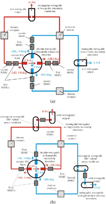
We assume the radiation incoming into the OMT receiver module is carried from a feed-horn whose circular waveguide output matches the input circular waveguide of the OMT. Figure 1 shows our two OMT design concepts. A discussion on waveguide modes and architectures of waveguide transitions will be given in sub-section 2.1. We use two couples of orthogonal balanced probes
located symmetrically at the circular waveguide inputs to extract the two orthogonally polarized incoming signals and couple them to four independent RF circuitries: we highlight this part in Figure 1 as “circular waveguide to four-probe microstrip transition”.
(a)
(b)
Figure 1. Design concept of active planar OMT showing the input “circular waveguide to four-probe microstrip transition”, the low-noise amplification stages, the crossover section, the dummy overpass and the hybrid power combiners. The red and blue lines identify, respectively the electrical paths of the horizontal polarization (H-Pol) and of the vertical polarization (V-Pol) channels. a) “8-ampConf”: planar OMT configuration requiring eight MMICs, where two cascaded MMICs are used at each of the four outputs of the circular waveguide to four-probe microstrip transition. b) “6-ampConf”: planar OMT configuration requiring six MMICs, where one MMIC is used at each of the four outputs of the circular waveguide to four-probe microstrip transition and the second MMIC is used at the output of
the rectangular waveguide 180° hybrid power combiner. The four antenna probes are located approximately a quarter wavelength (~λg/4) in front of a non-tunable circular waveguide backshort (RF short circuit) in order to provide broadband performance. An amplification section composed of one or two cascaded MMICs is placed close to each output of the circular waveguide to four-probe microstrip transition. As the RF signals entering each couple of symmetric probes are equally split out-of-phase it is necessary to recombine them in a 1800 hybrid power combiner through amplitude-matched and phase-matched electrical paths as to avoid in-band resonances. The amplitude and phase balance depends on the combined effects of the transmission lines and of the MMICs. In particular, the gain and phase of the MMICs placed on opposite arms of each polarization channel would need to be matched. Each of the OMT designs includes two 1800 hybrid combiners, one per each of the polarization channels. The hybrids, indicated in Fig. 1 as “rectangular waveguide to two-probe microstrip transitions” recombine the amplified out-of-phase signals from the MMICs into oval waveguide outputs. Each transition is composed of two balanced in-line probes placed into the E-plane of the rectangular waveguides. The antenna probes are located at ~λg/4 in front of a rectangular waveguide backshort to provide wideband performance. Because the transmission lines carrying the signals of the two orthogonal channels are located on the same circuit plane they would cross their paths before recombination in the hybrid. To solve this problem we employ a “crossover” section allowing the two orthogonally oriented transmission lines to cross-each other. In addition, cross-each OMT designs include a dummy overpass, one for each polarization lines, to compensate for the added electrical length due to the crossover section. The proposed design concept can allow operation across the 75-116 GHz frequency range, corresponding to a ≈43% relative bandwidth.
2.1 Waveguide modes and design details of
the OMTs
The OMT circular waveguide input allows propagation of the two orthogonal polarization modes (TE11 fundamental
modes) associated with the Horizontal Polarization (H-Pol) and with the Vertical Polarization (V-(H-Pol) RF signals. Each of the two modes is coupled independently through the circular waveguide to four-probe microstrip transition based on quartz microstrip probes.
If “r” indicates the radius of a circular waveguide, the cut-off wavelength of the TE11 fundamental mode is λg=3.412
× r [15]. Consequently, the cut-off frequency of such mode is νc=58.56 GHz for r=3 mm. In theory, the two
higher order modes of the circular waveguide, the TM01
and the TE21, can be excited by the discontinuities
generated by the microstrip probes inside the waveguide itself. However, their excitation is avoided if the four-fold symmetry of the structure is maintained. Planar OMT designs with two or three non-symmetrical probes located inside a circular waveguide are discussed in [16]. As these OMT configurations break the four-fold symmetry, the
fractional bandwidth of the devices is considerably narrowed due to the excitation of the TM01 mode. The
four-fold symmetrical configuration guarantees that the single TE11 mode bandwidth in circular waveguide can
extend up to a relative value of 66%, νc(TM11)/
νc(TE11)=2.08. Each orthogonal polarization is split in two
out-of-phase components by the circular waveguide to four-probe microstrip transition. The outputs of such transitions are amplified by one or two MMIC amplifiers with ≈20 dB gain each. The signals from the MMIC outputs are recombined by the rectangular waveguide to two-probe microstrip transition (Figure 1-a) or by the rectangular waveguide 180° hybrid power combiner (Figure 1-b). The maximum bandwidth of the transition is bounded by the single mode operating range of the WR10 rectangular waveguide, set at the low frequency end by the cut-off frequency of the TE10 mode (νc=59.01 GHz)
and at the high end by that of the next higher mode, the TE20 (νc=118.03 GHz). Thus, the single TE10 mode
bandwidth in WR10 rectangular waveguide extends up to a relative value of one octave, i.e. νc(TE20)/νc(TE10)=2.
The main role of the amplification stage located at each outputs of the circular waveguide to four-probe microstrip transition is to reduce the noise temperature of the following receiver stages, as their noise contribution is divided by the gain of such amplifiers. Assuming that the circuitry and receiver parts following the amplification adds little or no extra noise, the receiver noise temperature referred to the active OMT waveguide input will only depend on the losses of the circular waveguide and of the first microstrip transmission as well as on the noise temperature of the MMIC LNA, which depends on the impedance presented at its input.
3. Architectures of the two planar OMTs
Starting from the design concepts illustrated in the previous section we developed two different active planar OMT architectures. The first configuration, named “8-ampConf,” has an amplification stage composed of two cascaded MMICs, installed at each output of the circular waveguide to four-probe microstrip transition. This configuration uses eight MMICs in total (Figure 1-a). The second configuration, named “6-ampConf,” has an amplification stage composed of only one MMIC at each output of the circular waveguide to four-probe microstrip transition. This second configuration requires an additional amplification stage composed of one MMIC located at the input of the rectangular waveguide to single-probe microstrip transitions, (Figure 1-b). Thus, “6-ampConf” uses six MMICs in total. In short, the major differences between the two configurations are on the number and position of used MMICs.
The two configurations are based on the same technological approach: the input and outputs lines of the OMT use a waveguide transmission line, whereas the planar circuitry parts employ different transmission line types: microstrip, coplanar and stripline. The planar transmission lines are realized on different substrate types. The antenna probes and microstrip lines are
implemented on 80 µm thick quartz substrate (dielectric constant ɛr=3.8). A 50 Ω impedance is obtained with a
microstrip width of 0.17 mm resulting in 0.08 dB/mm at 100 GHz (λg=1.75mm, tan δ=0.0013). The transmission lines employed after the first MMIC stage are made in stripline technologies and are based on a Teflon substrate (from Rogers Corp.). The estimated electrical losses of the device upstream the MMIC stages are due to the circular waveguide input and to the first quartz chip with Gold antenna probes. Assuming to use Aluminum blocks with a conductivity of t 3.4×10⁷ S/m and a conductivity of
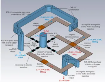
the Gold of 4.1 ×10⁷ S/m we obtain about 0.165 dB of total losses. A possible radio frequency deployment of the concept design proposed in Fig. 1a is shown in Fig. 2. The design employs WR-10 E-plane bends and WR-10 H-plane bends with oval waveguide outputs parallel to the circular waveguide input.
Figure 2: A possible design concept of active planar OMT with 8 MMIC LNAs (“8-ampConf”).
4. Mechanical Design
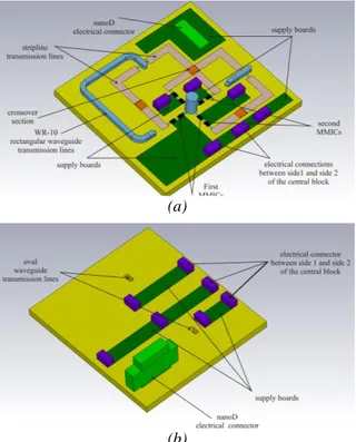
The MMIC chips and DC power supply boards are integrated into a mechanical body assembled in three Aluminum blocks (Fig. 3 and Fig. 4)
Figure 3: 3D view of the bottom part of the OMT receiver module showing the orientation of the two oval output waveguides. The external dimension of the assembled blocks is 40 x 44 x 13 mm3.
The assembled OMT with eigth MMIC chips, “8-ampConf,” has external size of 40 x 44 x 13 mm3. It
features a circular waveguide input on the top block and the two parallel oval waveguide outputs in the bottom block. The inter-axis distance between the two oval waveguide outputs in the assembled OMT (24.15 mm) was chosen to allow two standard UG387 flanges to be attached side-by-side with a minimum extra spacing between them. A nano-D connector is housed in the bottom block. All the MMICs and their DC electrical circuitries are arranged in the central block. The OMT unit can be easily manufactured with a numerically controlled CNC milling machine.
(a)
(b)
Figure 4: Two different 3D views of the central block. a) Side 1 view, in contact with the top block: the RF transmission lines and some electrical supply boards are arranged on this block side. b) Side 2 view, in contact with the bottom block: the electrical supply boards necessary for the DC connections of all circuit parts are arranged on this block side.
5. Acknowledgements
This project has received funding from the European Union’s Horizon 2020 research and innovation programme under grant agreement No 730562.
6. References
1. J. W. M. Baars, B. G. Hooghoudt, P. G. Mezger, M. J. de Jonge, “The IRAM 30-m millimeter radio telescope on Pico Veleta, Spain,” Astronomy and Astrophysics, 175, pp. 319-326, 1987.
2. J. D. Kraus, “Radio Astronomy”, McGraw-Hill Book Company, 1966;
3. A. Navarrini, R. L. Plambeck, “Orthomode Transducers for Millimeter Wavelengths,” Proceedings of URSI North American Radio Science Meeting, invited, Ottawa, Canada, July 22-26, 2007.
4. A. M. Boifot, E. Lier, T. Schaug-Pettersen, “Simple and broadband orthomode transducer” IEEE PROCEEDINGS, Vol. 137, Pt. H, No. 6, December 1990, pp. 396-400.
5. A. Navarrini and R.L. Plambeck, “A Turnstile Junction Waveguide Orthomode Transucer,” IEEE Trans. Microwave Theory Tech., 54(1),272-277 (2006).
6. A. Navarrini, R. L. Plambeck and D. Chow, “A Turnstile Junction Waveguide Orthomode Transducer for the 1 mm Band,” Proceedings of the 16th International Symposium on Space Terahertz Technology, Gothenburg, Sweden, May 02-04, 2005.
7. A. Navarrini, A. Bolatto, R. L. Plambeck, “Test of 1 mm Band Turnstile Junction Waveguide Orthomode Transducer,” Proceedings of the 17th International Symposium on Space Terahertz Technology, Paris, France, May 10-12, 2006.
8. G. Pisano, L. Pietranera, et al. , “A Broadband WR10 Turnstile Junction Orthomode Transducer,” IEEE Micr. Wireless Comp. Lett., Vol. 17, n. 4, Apr. 2007.
9. A. Navarrini, R. Nesti, “Symmetric reverse-coupled waveguide orthomode transducerfor the 3mm band,” IEEE Trans. Microw. Theory Tech., vol. 57, no. 1, pp. 80-88, Jan. 2009.
10. A. Navarrini, R. Nesti, “Dual-side backward coupler waveguide orthomode transducer for the 3 mm band,” Proc. of SPIE Astronomical Telescope and Instrumentation, Millimeter and Submillimeter Detectors and Instrumentation for Astronomy IV, Vol. 7020, 70202M, Marseille, France, 23-28 June 2008.
11. G. Valente, G. Montisci, T. Pisanu, A. Navarrini, P. Marongiu, G. A. Casula, "A Compact L-Band Orthomode Transducer for Radio Astronomical Receivers at
Cryogenic Temperature", IEEE Trans. Microw. Theory Tech, vol. 63, no. 10, October 2015.
12. G. Valente, A. Navarrini, “Design of Planar Orthomode Transducer for 84-116 GHz,” Proceedings of 24th International Symposium on Space Terahertz Technology, Groningen, The Netherlands, 8-10 Apr 2013. 13. G. Engargiola, R. L. Plambeck, “Tests of a planar L-band orthomode transducer in circular waveguide”, Rev. Sci. Instrum., vol. 74, no. 3, pp. 1380-1382, Mar. 2003. 14. G. Engargiola, A. Navarrini, “K-band orthomode transducer with waveguide ports and balanced coaxial probes”, IEEE Trans. Microw. Theory Techn., vol. 53, n. 5, pp. 1792-1801, May 2005.
15. David M. Pozar, “Microwave Engineering”, Wily John Wiley&Sons, Inc, 205
16. R. W. Jackson, "A planar orthomode transducer", IEEE Microw. Wireless Compon. Lett., vol. 11, no. 12, pp. 483-485, Dec. 2001.