Growth of diborides thin films on different substrates by pulsed laser ablation
V. Ferrando
a,⁎
, C. Tarantini
a, P. Manfrinetti
b, I. Pallecchi
a, M. Salvato
c, C. Ferdeghini
aa
CNR-INFM-LAMIA, Dipartimento di Fisica, Via Dodecaneso 33, 16146 Genova, Italy
b
CNR-INFM-LAMIA, Dipartimento di Chimica e Chimica Industriale, Via Dodecaneso 31, 16146 Genova, Italy
c
Dipartimento di Fisica, Università di Roma“Tor Vergata” via della Ricerca Scientifica, I-00133, Roma and Laboratorio Regionale SuperMat CNR-INFM, Baronissi (SA) I-84081, Italy
Received 17 May 2005; received in revised form 19 October 2005; accepted 5 April 2006 Available online 24 May 2006
Abstract
The growth of scandium, titanium and zirconium diborides thin films by pulsed laser ablation technique on different substrates has been studied. In situ reflection high energy electron diffraction and ex situ X-ray diffraction analyses indicate that the films are strongly c-axis oriented on all the substrates and also epitaxial, apart from Si(111), where the in plane orientation is poor. Atomic force microscopy imaging reveals a flat surface in all the epitaxial samples, with roughness lower than 1 nm. The results on silicon carbide and sapphire are very promising for using these materials as buffer layers in magnesium diboride thin films growth, especially to improve epitaxy and to prevent oxygen diffusion from the substrate, and also to study the influence of lattice strain on MgB2critical temperature.
© 2006 Elsevier B.V. All rights reserved.
Keywords: Diborides; Thin films growth
1. Introduction
Known since the fifties, metal diborides have been used in a large number of applications, in particular as highly corrosion resistant coatings materials, thermal barriers in chemical reactors and diffusion barriers on silicon in semiconductors technology[1]due to their hardness, high melting points, good corrosion resistance and low friction coefficient. Diborides films, in particular zirconium and titanium diboride films, have been produced by various techniques[2–6](i.e. chemical vapor deposition, physical vapor deposition and sputtering), but in general the above mentioned applications do not need epitaxial samples. Actually, ZrB2 has been grown epitaxiallly by chemical vapor deposition and used as buffer layer for group III nitrides [7], and recently, after the discovery of supercon-ductivity in magnesium diboride[8], few groups were able to obtain epitaxial TiB2thin films[9,10]to employ them as buffer layer for MgB2deposition. The interest of epitaxial growth of diborides resides first of all in their AlB2-type crystal structure, the same of magnesium diboride that can surely improve
epitaxy of MgB2. Furthermore, they could act as a barrier, avoiding the oxygen diffusion from the substrate to the superconducting film. It has been shown that, during the annealing of MgB2films at high temperature, such as 900 °C
[11,12], an interlayer of MgO, which could have a negative
influence on superconducting properties of the samples, is formed at the interface between the substrate and the film. Sapphire in fact is not very stable at temperatures higher than 850 °C, starting to release oxygen.
Another intriguing reason to have epitaxial diborides films is to induce a tensile strain in magnesium diboride, so that an enhancement of critical temperature is produced. Pogrebnyakov et al. [13,14] showed that films grown by hybrid physical chemical vapor deposition on silicon carbide can have Tcabove 41 K, a value higher than the bulk one, due to the tensile strain of a-axis caused by the thermal expansion of SiC substrate. Another possible way to get similar effects could be to grow the films on a material with larger in plane parameter so that the tensile strain is produced directly by the lattice mismatch. Actually, among diborides of the family M-B2, there are compounds with a parameter larger than MgB2 (ZrB2 and ScB2)[15]that can be used as buffer layers to observe a raise in Tc. The lattice parameters of some non-volatile diborides in ⁎ Corresponding author.
E-mail address:[email protected](V. Ferrando).
0040-6090/$ - see front matter © 2006 Elsevier B.V. All rights reserved. doi:10.1016/j.tsf.2006.04.008
bulk form together with those of MgB2 are summarized in
Table 1.
Moreover, due to the absence of volatile elements, in principle, they can be grown epitaxially at high temperature with standard pulsed laser deposition techniques, with good surface morphology, without post annealing process. First attempts to grow magnesium diboride on ZrB2 by two-step technique [16] showed that the buffer layer is an effective barrier for oxygen interdiffusion, helping epitaxy of the superconducting film. A small increase of the a parameter of MgB2has been found, but the eventual enhancement of Tccould not be observed, owing to the intrinsic disorder caused by growth method. A technique to grow extremely pure and clean MgB2 film is therefore needed to observe this effect and probably the best one could be HPCVD.
In this paper, we present a comparative study of the growth of different diborides by pulsed laser ablation. We will show how it is possible to deposit epitaxial TiB2, ZrB2and ScB2thin films with a very smooth surface suitable to be used as buffer layers in MgB2 growth, with the aim of avoiding oxygen contamination or induce tensile strain in the superconducting phase.
2. Experimental details
ZrB2, ScB2and TiB2were grown by pulsed laser deposition in the experimental apparatus already described in detail elsewhere [17], consisting of a vacuum chamber and of an KrF excimer laser (wavelength λ=248 nm). The starting pressure was as low as 10− 8Pa without any buffer gas for all the materials and reflection high energy electron diffraction (RHEED) was used to monitor in situ the growth of the film during deposition. This analysis gives important information about the ordering and the quality of the surface and also about the presence of some in plane orientation. For zirconium and titanium diboride, commercial stoichiometric and dense targets (Superconducting Components, Inc.) were employed. For ScB2 instead, commercial targets were not available, so we used a home-made pellet prepared by direct synthesis. Taking into consideration the AlB2-type hexagonal crystalline structure of these diborides, we used substrates with the same surface cell symmetry, in particular, c-cut sapphire (a = 0.476 nm), silicon carbide (a = 0.3081 nm) and silicon(111) (cubic structure with a = 0.3543 nm).
In order to find the best deposition conditions, we scanned the space of parameters (laser frequency, density of energy and substrate temperature) for all the diborides.
The substrate temperature was varied between 650 °C and 950 °C, the density of laser energy between 1.5 and 5 J/cm2, and
the repetition rate between 1 and 10 Hz, low enough to give time to adatoms to diffuse on the substrate surface. The deposition rate was evaluated by X-ray reflectivity measure-ments and was extremely low, about 0.02 Å/pulse for TiB2and ScB2and 0.05 Å/pulse for ZrB2.
After the growth, the samples were both quenched to room temperature or slowly cooled down to improve the crystalliza-tion of the phase, but no significant difference in the final quality of the films ascribing to the cooling method was observed. The growth of the films was monitored in situ by an ER 2035 K RHEED system by Staib Instrumente at 20 kV of beam energy and with an incidence angle of ∼ 1°, and the RHEED diffraction patterns were acquired by a CCD camera. The structural characterization was carried out by standard Cu-Kα X-ray diffraction techniques in Bragg-Brentano geometry using a Philips X-Pert diffractometer. Finally, the surface of the films was studied by atomic force microscopy (AFM) in contact mode using a silicon tip (scan speed 256 lines, sampling rate 1 Hz) in order to estimate the RMS roughness, which is extremely important to employ these samples in multilayer structures.
3. Results and discussion
The best growth conditions for titanium, scandium and zirconium diboride are summarized inTable 2. The epitaxial growth of all these diborides seems to be mostly influenced by the deposition temperature. For titanium diboride for instance, at temperatures lower than 700 °C and higher than 830 °C, the intensity of the peaks in the X-ray patterns is extremely low and RHEED signal rapidly disappears after few tens of angstrom of deposition, suggesting that the growth is not ordered or that the film surface is rough. Between 700 and 830 °C instead, the samples resulted to be strongly oriented along the c-axis and also with a single in plane orientation. For zirconium and scandium diboride, higher temperatures were required to get epitaxial samples; in particular, ZrB2best films were deposited at 900–950 °C, while ScB2at 875–900 °C. In temperature ranges others than the above ones, the films may be c-axis oriented, but no preferential in plane orientation was found. Concerning the laser frequency, only TiB2can be grown in an ordered way up to 10 Hz; in the other cases, too high repetition rates caused the loss of the RHEED signal during the growth.
It must be emphasized that in the case of ScB2the growth conditions are very critical and only few samples were found to be in plane oriented. In particular, the substrate temperature seems to be crucial for this compound and often samples Table 1
Lattice parameters of some non-volatile diborides, along with those of MgB2
Compound a-axis (nm) c-axis (nm)
TiB2 0.3038 0.3239
MgB2 0.3086 0.3524
ScB2 0.3147 0.3517
ZrB2 0.3169 0.3530
Table 2
Best growth parameters for diborides thin films Substrate temperature (°C) Density of energy (J/cm2) Laser frequency (Hz) Substrate TiB2 700–830 2.5 1–10 Al2O3, SiC ZrB2 900–950 2.5 3–5 Al2O3, SiC, Si(111) ScB2 875–900 2.5 3 Al2O3
grown nominally in the same conditions were only c-axis oriented instead of being epitaxial. The properties described in the following are referred to the best films of ScB2 and to standard samples of TiB2 and ZrB2, which showed a better reproducibility.
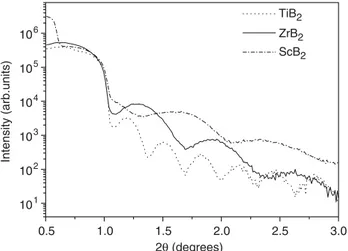
Fig. 1reports an example of X-ray reflectivity measurements
on films of the three materials. The good quality of the oscillations indicates that the surface is flat as it is also confirmed by AFM and RHEED images presented hereafter. The different periodicity of oscillation in the three samples represents the different thickness of the films, i.e. the larger is the periodicity, the thinner is the layer. The thickness of the samples presented in this paper is in the range 10–30 nm. The adhesion to the substrate seems to be good, even when the thickness is low. In fact, the samples were not degraded even when we measured them several months after the deposition.
RHEED analyses have been systematically carried out during the deposition of all the diborides. Fig. 2 shows examples of diffraction patterns for TiB2, ScB2 and ZrB2 films on different substrates; in particular, panels a, b, c and d present TiB2on SiC, ScB2on Al2O3, ZrB2on SiC and ZrB2on Si(111), respectively. In the panels, the upper picture is referred to the clean substrate, and then images of a 5 nm thick film and of the film rotated of 30° with respect to the electron beam are reported. In panel d, only the images of the ZrB2growth are reported, due to the fact that the clean silicon substrate was too rough and it did not give a good diffraction pattern.
The presence of bright spots arranged in a regular lattice indicates that the samples on silicon carbide and sapphire grow in a three-dimensional mode, but they have anyway a good crystallinity. Moreover, passing from the substrate to the film and then rotating the film with respect to the beam, the distance between the spots, which is proportional to the inverse of the distances between atoms in the lattice, changes. The ratio between the spacing of the two orientations of the films is exactly pffiffiffi3, which corresponds to the value expected for a rotation by 30° around the c-axis of an AlB2-type hexagonal structure. This is an evidence that TiB2, ScB2and ZrB2have a
single in plane orientation both on sapphire and on silicon carbide, as will be verified also by X-ray diffraction. Concerning the reciprocal orientation between the diborides and the two substrates instead, sapphire induces a 30° rotated growth of the film, which produces a lower lattice mismatch (on 3 × 4 supercell) than the hexagon on hexagon growth (on a 2 × 3 supercell), similarly to what observed in MgB2 [11,18]. The ratio between the distances of the spots of substrate and film is in fact inFig. 2b is proportional, as expected, to afilm/asapph
ffiffiffi 3 p
. In the samples on SiC (seeFig. 2a and c), this ratio is consistent with afilm/asapph, suggesting that hexagons of diborides and SiC grow one on top of each other, as expected considering the very low lattice mismatch (less than 1%). Similar results have been obtained for ZrB2and TiB2on sapphire, while we were not able to grow epitaxiallly ScB2on SiC.
Actually, we previously reported[9]for titanium diboride a “hexagon on hexagon” growth on sapphire at low deposition temperature (about 720 °C). The different in plane orientations observed here and in [9] can be induced by substrate temperature. The difference between lattice mismatches in the two orientations is not very big, and thus they can be competitive in particular conditions. We were not able to reproduce the same growth of[9]in this new series samples and, therefore, it is possible that the growth parameters are extremely
0.5 1.0 1.5 2.0 2.5 3.0 101 102 103 104 105 106 TiB2 ZrB2 ScB2 Intensity (arb.units) 2θ (degrees)
Fig. 1. Examples of reflectivity measurements for Zr, Sc and Ti diborides films. The different periodicity of the oscillations indicates the different thickness of the layers.
Fig. 2. RHEED diffraction patterns for (a) TiB2on SiC, (b) ScB2on Al2O3, (c)
ZrB2on SiC and (d) ZrB2on Si(111). In panels a, b and c, the three images from
top to bottom are referred to the clean substrate, to the 5 nm thick film and to the film rotated by 30° with respect to the electron beam. In panel d, only the images taken from the film are shown.
critical for the “hexagon on hexagon” growth. Except for the case of scandium diboride, whose deposition conditions are critical and not well reproducible, for the other two diborides, the RHEED patterns show bright contrast till the end of the deposition, suggesting that also increasing the thickness of the sample does not affect epitaxy and surface roughness. In view of its wide use in device applications, also Si(111) has been tested as a substrate for diborides. Actually, only zirconium diboride showed well defined and bright spots on this substrate (see panel d), suggesting a three-dimensional growth dominated by transmission through 3D islands; unfortunately, the lack of a good image from the clean substrate did not allow to verify the reciprocal orientation between Si(111) and ZrB2. Moreover, the distances between the spots before and after a 30° rotation of the film with respect to the electron beam have the expected ratio offfiffiffi
3 p
, even when scanning the whole surface of the film with the electron beam. This suggests that the crystalline islands of ZrB2 could have a preferential in plane orientation, which is however not very strong. It was impossible to get a strong signal in theΦ scan to prove the reciprocal orientation between the substrate and the film, and therefore we cannot surely claim for a complete epitaxy. AFM measurements gave a confirmation of what was suggested by RHEED analysis. Fig. 3 shows two images of a ZrB2 film deposited on SiC (panel a) and on Si (111) (panel b) taken on a 10 × 10 μm area. The difference between the two samples is clear: the film on silicon carbide has a flat surface, with RMS roughness of about 0.8 nm with few particulates coming from the target. On the contrary,
three-dimensional islands with average size of 1 μm are well evident on the film on Si(111), which has also high RMS roughness. It is possible that, at the high temperatures needed for the ZrB2 growth, some reconstruction phenomena, incompatible with the hexagonal structure of the film, occur at the Si surface. Considering all these effects, silicon seems not to be a good substrate for zirconium diboride and thus ZrB2/Si(111) films are not suitable as buffer layers for magnesium diboride.
Atomic force microscopy imaging on several titanium and scandium diborides revealed a very good quality of the surface with roughness lower than 1 nm and, in some cases, even lower than one crystalline cell, which is a fundamental requirement for using them as buffer layers.
The structural properties of all the diborides films have been investigated also by standard diffraction techniques.θ–2θ scans of ScB2 and ZrB2 films grown on sapphire (panels a and b, respectively) and of a ZrB2 film on Si(111) (panel c) are reported in Fig. 4. Results of X-ray diffraction on titanium diboride have been already reported in[9]. Apart from the two
Fig. 3. Atomic force microscopy images of a ZrB2film grown on silicon carbide
(a) and on Si(111) (b). The presence of micrometric islands is well evident in the film deposited on silicon.
101 103 102 105 104 106 20 25 30 35 40 45 50 55 60 102 103 104 Counts (arb.units) 102 103 104 105 2θ (degrees) 12.4 12.8 0 100 200 12.4 12.8 0 50 100 150 10 12 14 250 500 ZrB2 on Al2O2 (002) ZrB2 (001) ZrB2
*
*
*
*
ScB2 on Al2O3 (002) ScB2 (001) ScB 2 FWHM=0.2° θ (degrees) θ (degrees) FWHM=0.1° (001) ZrB2 (002) ZrB2 ZrB2 on Si(111) FWHM=2.2° θ (degrees)Fig. 4. X-ray diffraction patterns of a scandium (a) and zirconium (b) diboride films on sapphire and of ZrB2on Si(111) (c). In the insets, rocking curves around
reflections of aluminum due to the sample holder (marked by asterisks inFig. 4), only 00l reflections of AlB2-type structure are present, without secondary phases, indicating a good c-axis orientation of the films, confirmed also by the extremely narrow rocking curves around (001) peaks (FWHM = 0.1° for ZrB2, 0.3° for ScB2and 0.15° for TiB2; see insets ofFig. 4and Ref. [9]). Only the film on silicon shows poorer intensity of the peaks and a larger FWHM of the rocking curve, suggesting a lower quality of the phase crystallization and orientation. Furthermore, the finite size effects are well visible on both sides of (001) peak of ZrB2 on sapphire; the thickness evaluated from the spacing of the oscillations, 9.5 nm, is indeed compatible with that obtained from reflectivity on the same sample. Comparing these two kinds of measurements, we can conclude that ZrB2phase is well crystallized on Al2O3 and no amorphous or reacted layer is present at the interface between substrate and film. Although finite size effects have been observed only on ZrB2, the c-axis orientation of scandium diboride film is also very good, apart from a peak attributed to scandium oxide around 20–30°, probably due to the high deposition temperature; Sc2O3 in fact is extremely stable. From the position of (00l) peaks in films grown on sapphire, we calculated also the c-axis parameter for the three compounds; the average value is higher than the bulk value
(seeTable 1) in all the case, being (0.3530 ± 0.0005) nm for
ScB2, (0.3570 ± 0.0005) nm for ZrB2and (0.3270 ± 0.0005) nm for TiB2. This enhancement of the c-axis can be related to the strain induced by the substrates during the growth; it is possible that, increasing the thickness of the films, the lattice parameters relax coming back to the bulk values. Unfortu-nately, due to the extremely low growth rate, it was impossible to grow thicker samples.
Concerning the in plane orientation,Φ scans confirmed the results got from RHEED analysis. Films deposited on Al2O3 grow with a rotation of 30° with respect to the substrate, while those on silicon carbide have hexagons one on top of each other. An example of aΦ scan performed on a TiB2film on sapphire substrate is shown inFig. 5. As expected, the peaks of the film
(lower panel) are shifted of 30° with respect of those of the substrate; their width of about 5° indicate that some in plane misalignment, probably due to strain, is present.
The use of diborides as buffer layers in MgB2 deposition requires, together with epitaxy and smooth surfaces, also a good thermal stability of the phase at high temperatures. Both annealing process in the two-step technique and HPCVD are performed at temperatures between 700 and 900 °C. To verify the stability of these films, three samples were closed in a tantalum crucible under argon and heated up at 850 °C for 1 h to simulate the heat treatment in Mg vapor used for MgB2[11]. A second X-ray characterization after the annealing did not show any difference in the diffraction patterns; only a small shift of the c-axis toward the bulk values was observed, indicating a relaxation of the lattice strain.
From an electrical point of view, the resistivity has been measured by standard four probe technique on several films of all the three diborides, also as a function of temperature. All of them showed a metallic behavior, with resistivity at 300 K between 40 and 100μΩ cm for TiB2, between 100 and 200μΩ cm for ScB2and few mΩ cm for ZrB2. These values are higher than those reported in literature for single crystals [19], especially for zirconium diboride, probably due to the strong nanostructuration of the films.
4. Conclusions
We studied the growth of zirconium, scandium and titanium diborides thin films by pulsed laser deposition on different substrates. A careful structural characterization of the films, carried out by RHEED and X-ray diffraction, revealed that all the diborides grow strongly oriented along the c-axis and epitaxial on sapphire and silicon carbide, while silicon induces the formation of three-dimensional islands, with a poor in plane alignment and a rough surface. On the contrary, AFM imaging showed the good quality of the surface of diborides films deposited on the other substrates, with RMS roughness lower than 1 nm, which is very promising for the use of these materials as buffer layers in superconducting magnesium diboride growth. Finally, the films resulted to be stable at high temperature, being a possible barrier for oxygen contamination of MgB2.
References
[1] R.G. Munro, J. Res. Natl. Inst. Stand. Technol. 105 (2000) 709. [2] M. Mukaida, T. Goto, T. Hirai, J. Mater. Sci. 26 (1991) 6613. [3] C. Courtois, J. Desmaison, H. Tawil, J. Phys. IV 1 (1991) 657. [4] I. Zergioti, G.H. Haidemenopoulos, C. Fotakis, Appl. Phys., A Mater. Sci.
Process. 69 (1999) S427.
[5] J.F. Pierson, T. Belmonte, D. Czerwiec, H. Hertz, Thin Solid Films 359 (2000) 68.
[6] C. Mitterer, J. Appl. Chem. 133 (1997) 279.
[7] J. Tolle, R. Roucka, I.S.T. Tsong, C. Ritter, P.A. Crozier, A.V.G. Chizmeshya, J. Kouvetakis, Appl. Phys. Lett. 82 (2003) 2398.
[8] J. Nagamatsu, N. Nakagawa, T. Muranaka, Y. Zenitani, J. Akimitsu, Nature 410 (2001) 63.
[9] V. Ferrando, D. Marré, P. Manfrinetti, I. Pallecchi, C. Tarantini, C. Ferdeghini, Thin Solid Films 444 (2003) 91.
0 50 100 150 200 250 300 350
(101) TiB2
Intensity (arb.units)
θ (degrees)
(024) Al2O3
Fig. 5.Φ scan around 101 reflection of TiB2and on the sapphire substrate. Peaks
spaced of 60° are visible in the film pattern, according to the six-fold symmetry of TiB2structure; they are rotated by 30° with respect to the substrate peaks.
[10] H.Y. Zhai, H.M. Christen, C. Cantoni, A. Goyal, D.H. Lowndes, Appl. Phys. Lett. 80 (2002) 1963.
[11] V. Ferrando, S. Amoruso, E. Bellingeri, R. Bruzzese, P. Manfrinetti, D. Marrè, N. Spinelli, R. Velotta, X. Wang, C. Ferdeghini, Supercond. Sci. Technol. 16 (2003) 241.
[12] C. Ferdeghini, V. Ferrando, C. Tarantini, E. Bellingeri, G. Grasso, A. Malagoli, D. Marrè, M. Putti, P. Manfrinetti, A. Pogrebnyakov, J.M. Redwing, X.X. Xi, R. Felici, E. Haanappel, IEEE Trans. Appl. Supercond. 15 (2005) 3234.
[13] A.V. Pogrebnyakov, J.M. Redwing, E.M. Jones, X.X. Xi, S.Y. Xu, Qi Li, V. Vaithyanathan, D.G. Schlom, Appl. Phys. Lett. 82 (2003) 4319. [14] A.V. Pogrebnyakov, J.M. Redwing, S. Raghavan, V. Vaithyanathan, D.G.
Schlom, S.Y. Xu, Qi Li, D.A. Tenne, A. Soukiassian, X.X. Xi, M.D. Johannes, D. Kasinathan, W.E. Pickett, J.S. Wu, J.C.H. Spence, Phys. Rev. Lett. 93 (2004) 14.
[15] P. Villars, L.D. Calvert, Pearson's Handbook of Crystallographic Data for Intermetallic Phases, 2nd ed., ASM International, Materials Park, OH, 1991.
[16] V. Ferrando, C. Tarantini, E. Bellingeri, P. Manfrinetti, I. Pallecchi, D. Marré, O. Plantevin, M. Putti, R. Felici, C. Ferdeghini, Supercond. Sci. Technol. 17 (2004) 1434.
[17] M.R. Cimberle, C. Ferdeghini, G. Grassano, D. Marré, M. Putti, A.S. Siri, F. Canepa, IEEE Trans. Appl. Supercond. 9 (1999) 1727.
[18] X. Zeng, A.V. Pogrebnyakov, A. Kothcharov, J.E. Jones, X.X. Xi, E.M. Lysczek, J.M. Redwing, S. Xu, Qi Li, J. Lettieri, D.G. Schlom, W. Tian, X. Pan, Z.K. Liu, Nat. Mater. 1 (2002) 35.
[19] A. Shutou, T. Masui, H. Tsuda, H. Mabuchi, K. Morii, Mater. Lett. 45 (2000) 143.