and P. Vallerand(1)
(1) CNRS/IN2P3/LAL Orsay, IJCLab - Orsay, France
(2) CEA/IRFU - Saclay, France
received 2 March 2020
Summary. — Measuring the Time Of Flight (TOF) of particles with picosecond (ps) precision opens new fields for particle physics and medical instrumentation. It indeed permits the localization of particle production with a few mm precision which is of direct use for PET scanners, but also permits associating particles com-ing from a common primary interaction in the case of high background in physics experiments. The progress in ultra-fast digitizing electronics (including high-end oscilloscopes) demonstrated that ps timing accuracy can be reached simply by di-rectly sampling the detector signal at high rates and extracting time information by interpolation of the samples located in and around the leading edge of the signal. But when one has to deal with high integration levels, large number of channels, or high counting rates, a compact solution is mandatory and the new concept of Waveform Time to Digital Converter (WTDC) permits facing all these constraints in a very compact and powerful way. This paper will summarize the requirements for high-precision time measurements, explain the concept of WTDC, then focus on the SAMPIC ASIC and its associated boards and modules. The main characteristics will be described as well as the performances obtained on test benches and when coupling the modules to fast detectors.
1. – Introduction
Time stamping with ps accuracy is a technique opening new fields for particle physics and medical instrumentation. It indeed permits the localization of vertices with a few mm precision, thus helping associating particles coming from a common primary interaction even in a high background. It can also be used for particle identification based on Time-of-Flight techniques. The progress in ultra-fast digitizers (including high-end oscilloscopes) demonstrated that ps timing accuracy can be reached simply by sampling the detector signal at high rates and extracting time information by interpolation of the samples
(∗) Corresponding author. E-mail: [email protected]
based on standard Analog to Digital Converters (ADCs), which can be interleaved in order to virtually increase their sampling frequency. As evoked above, the digitized waveform can be used to extract time information but the sampling rates required for high-precision measurement on fast signals sit far above 1 GS/s. Consequently, the huge local data rate per channel at the output of the ADCs (far above 10 Gbits/s) becomes a real problem, if not a showstopper, especially for large-scale systems.
2.2. Time to digital converters. – This is not the case with the standard Time to Digital Converters (TDCs), which are commonly used for time measurement in physics experiments. They are designed either as dedicated ASICs or integrated inside high-end FPGAs. Here, the information is concentrated into a simple digital integer value, thus reducing drastically the quantity of information, which is adequate for large-scale measurements. But TDCs do not provide information on the waveform, except under the derivate form of Time Over Threshold (TOT) for those able to measure both edges of the signal. Anyhow, in this case, the precision on the amplitude and charge of the signal remains poor.
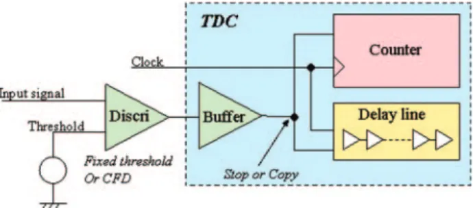
The standard digital TDCs are usually based on the association of a coarse time counter running on the main clock and of Delay Line Loops (DLLs) interpolating the latter (see fig. 1). In order to improve the resolution, the DLLs can be smartly inter-leaved, introducing a third stage for the fine measurement. Resolution is given by the DLL step but it is usually limited by stability of calibration or environmental effects. Actually, the weak point of the TDC is to have a strictly digital input, which means that a discriminator has to be present to transform the analog signal into digital. This discriminator introduces additional jitter and effects related to time walk, which is the dependency of the threshold crossing time on the pulse amplitude. The overall timing resolution is consequently degraded to the quadratic sum of the discriminator and TDC respective timing resolutions, making it difficult to go below 20 ps rms [2]. Moreover, the power consumption of the discriminator required to reach good timing performance is naturally high. Another characteristic of a TDC is that each channel is self-triggering.
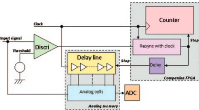
Fig. 2. – Principle of a TDC based on a fast analog memory and a FPGA.
This, associated with the small amount of data per hit, permits reaching high front-end counting rates (far above MHz). But in the presence of large counting noise like with Silicon Photo-Multipliers (SiPMs), the hit rate may become saturated by noisy hits. Dedicated buffers are thus usually present at the TDC output for selecting hits based on an external trigger system like in the large particle physics experiments where the first-level general trigger sorts the events.
2.3. Analog memories. – In order to get both waveform and time information, time measurement can be based on a mix of an analog memory and a FPGA (see fig. 2). Fast analog memories using Switched Capacitor Arrays (SCAs) nicely fit this scheme especially in terms of power, space and money budgets [3-5]. They sample the input signal, which can now be analog and permit performing an interpolation of the samples recorded on the latter. The discriminator is not anymore in the critical timing path. Time information is given by association of the timestamp counter (few ns step), of the DLL locked on the clock to define region of interest (100 to a few 100 s ps minimum step), and finally of the samples of the waveform: their interpolation will give a precision of a few ps rms. This requires a precise calibration of the time integral non-linearity. This ultimate time resolution can be reached even on small analog signals (a few tens of mV). Another advantage of recording the waveform resides in the cases where the shape of the detector signal (especially the leading edge) carries extra information in addition to direct measurements (time, amplitude, etc.). The main drawback of the SCAs is their readout dead-time (a few tens to 100 us depending on the number of samples read) which rapidly becomes a limitation at high rates. Moreover, the channels are usually not independent and commonly triggered and readout like in an oscilloscope.
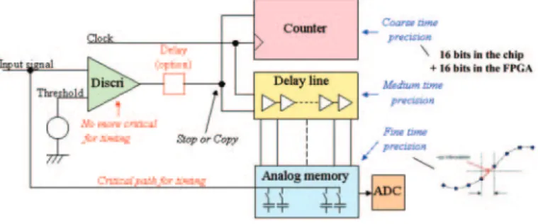
2.4. The new concept of Waveform TDC . – In order to take benefit of both waveform sampling and TDC structure, a new patented concept was introduced in 2009: the Wave-form TDC [6] (see fig. 3). Here, an analog memory is added in parallel with the delay line of the TDC. Moreover, the discriminator and the ADC are also integrated. This permits recording short waveform slices including the leading edge. Different methods can then be used for time extraction, like constant fraction discrimination or cross-correlation [7, 8]. A main feature with respect to SCAs is that all the channels are now independent like in a TDC, but they can also be triggered commonly if needed.
Fig. 3. – Principle of a Waveform TDC.
3. – The SAMPIC Waveform TDC
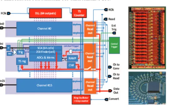
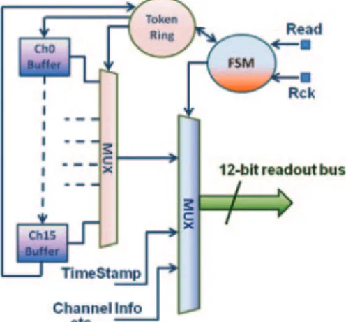
3.1. Global description. – An ASIC has been developed based on this new concept: it is called SAMPIC (Sampling Analog Memory for PICosecond time measurement). The first prototype was delivered in 2013. It houses 16 channels whose inputs directly receive the (externally amplified) analog signal coming from the detector, via an AC-coupling located on the board. The main elements of the chip architecture, depicted in fig. 4, are listed below:
• 16 single-ended channels, each equipped with a discriminator with programmable
threshold, independent and self-triggering.
• 64 analog switched-capacitor-based sampling cells per channel.
• One 7 to 11-bit ADC per cell (equivalent total of 1024 on-chip ADCs). • One common 16-bit gray counter (up to 160 MHz) for coarse time stamping. • One common 64-step DLL, servo-controlled to the clock period of the
aforemen-tioned gray counter, and providing sampling frequencies between 1 and 10 GS/s.
• One other common 11-bit gray counter running up to 1.5 GHz, used for the
mas-sively parallel Wilkinson ADC.
• One central trigger block.
• One 12-bit LVDS readout bus (potentially running up to 400 MHz). • A SPI interface for internal registers configuration.
The time tagging sequence for a given channel is driven by the discriminator. When it fires, the chip catches the state of the counter output (coarse timestamp, down to 6.4 ns steps) and that of the DLL (medium precision, down to 100 ps steps). Waveform sampling is then stopped, and the eventual interpolation between the analog samples will give the few ps time precision.
Figure 4 shows the layout and the implementation of the chip on its board. Its main characteristics are the following. Technology: CMOS 0.18 um. Size: 8 mm2. Package:
Fig. 4. – Left: Schematic diagram of SAMPIC chip. Right top: layout of SAMPIC V3D. Right bottom: the chip mounted on the board.
3.2. Main blocks. –
3.2.1. Input block. Each channel is equipped with an input block (see fig. 5) which permits either feeding the analog memory directly via a bypass switch, or passing through a signal translator. This permits translating any kind of digital signal (even differential) and performing standalone calibrations.
3.2.2. Analog memory. The chip has been designed to offer a signal bandwidth above 1 GHz and a usable dynamic range of 1 V. A special design has been studied in order to ensure a good quality (constant bandwidth and constant tracking duration) over all the 64 samples (even those located after trigger). The analog memory is a circular buffer
Fig. 6. – Principle of ADC conversion (auto-conversion mode).
so it is continuously writing until triggering, the oldest cells being overwritten after one turn. As mentioned previously, when trigger occurs (optionally after a postrig delay), the sampling is stopped and the position of the write pointer is tagged in the analog memory. This information is used for medium precision timing but also as a basis for the optional Region of Interest (RoI) mode of readout (only few cells read starting from a programmable offset from the trigger) for minimizing the readout deadtime.
3.2.3. Analog to digital conversion. The schematic principle of the analog to digital conversion is shown in fig. 6. By default, the auto-conversion mode is used. In this case, the gray counter is running continuously. The channel ADC ramp is launched immediately after the trigger and the value of the counter will be latched twice: once commonly at start of ramp, the second time in each cell when the ramp crosses the voltage stored. Both values are memorized and the difference will give the signal amplitude. The channel is ready for recording a new event as soon as all cells have been converted. Conversion time depends on the signal level, on the number of bits chosen for its precision and on the counter frequency: at 1.25 GHZ, the maximum time is of 1.5 us for 11 bits, down to 200 ns for 8 bits (even 100 ns for 7). This is actually the main contribution to the input dead time.
3.2.4. Readout philosophy. Readout is simply driven by Read and RCk signals (see fig. 7). Data is read channel by channel, with a rotating priority mechanism in order to avoid reading always the same channel. As evoked above, an optional RoI
Fig. 8. – Simplified triggering scheme.
readout is available to reduce the dead time (the number of cells read can be chosen dynamically). Event data is transmitted via a 12-bit parallel LVDS bus, whose standard speed is of 1.92 Gbits/s (160 MWords/s, potentially up to 4 Gbits/s). It is worthwhile to notice that a channel can be re-triggered once during its readout, since data register is a buffer stage. But the output multiplexor may become a source of deadtime at high rates.
3.2.5. SAMPIC triggering options. Each channel is equipped with one signal dis-criminator and one individual 10-bit DAC for setting the threshold (which can also be external). As shown in fig. 8, several trigger modes are programmable individually for each channel: local, external, central trigger (logical OR, double or triple multiplicity). Discriminator edge can be selected. Channels can be disabled. Post-trigger delay can be selected among 8 fractions of the sampling window. A common deadtime optional operation using a Fast Global Enable input is also available.
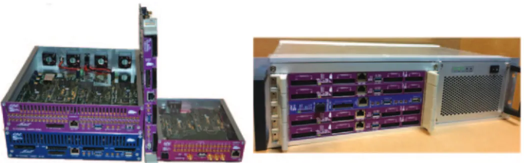
3.3. Acquisition modules and software. – In parallel to the chip design, we developed a family of electronics modules for SAMPIC. In most of them, the chip is mounted on mezzanine boards housing 16 channels, themselves mounted on mother boards which can hold 2 or 4 mezzanines: we thus designed native 32- or 64-channel modules. Input connectors are of MCX type. The modules are packaged in home-designed metal boxes (see fig. 9) and make use of an external compact AC/DC switching adaptor power supply. A 64-channel board with high density connectors has also been produced, and recently a 256-channel mini-crate. All boards and modules provide USB and UDP interfaces (copper or optical). Power consumption is as low as 5.5 W for 32 channels and 7.5 W for 64.
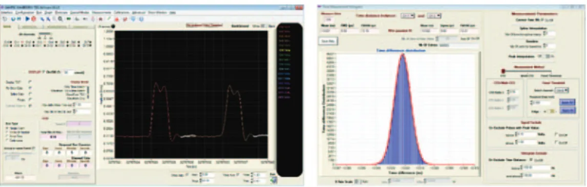
Fig. 10. – Left: the SAMPIC acquisition software in WTDC display mode. Right: time mea-surement panel.
We have also developed a graphical acquisition software which permits both the full characterization of the chips and the use of the modules in an autonomous way for test benches or small size experiments. It offers a special visualization for innovative WTDC mode. The latter permits visualizing the individual pieces of waveforms at their exact time location with respect to each other. This functionality is illustrated by the snapshot of fig. 10 on which the 2 waveforms plotted have different time origins. Many configuration menus and panels are available, which offers a great flexibility for all types of measurements. A panel fully dedicated to time measurement permits realizing real-time histograms of real-time difference between any pair of channels.
3.4. Calibration and measurements. –
3.4.1. Calibration philosophy. Characterization of this kind of circuit leads to dif-ferent types of calibrations. Our goal always is to find the set with the best perfor-mance/complexity ratio, but also to find the right set for the highest level of performance. SAMPIC actually offers very good performance with only two calibrations: ADC (cell pedestal and gain, with linear or parabolic fit); timing non-uniformity, also known as
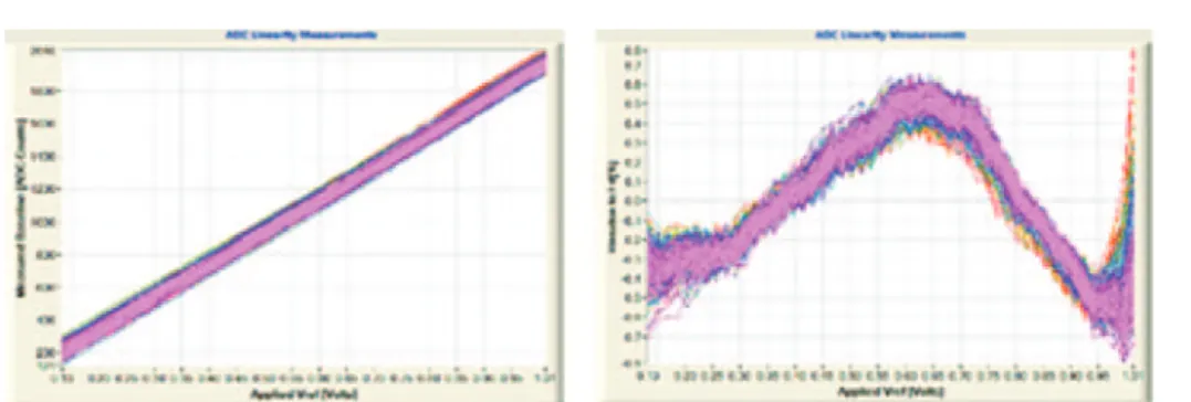
Fig. 12. – Left: ADC linearity calibration plot for all the cells from all the channels of a SAMPIC chip. Right: residues to linear fit of the data from the left plot.
time INL (one time offset per cell). This leads to a limited volume of standard calibra-tion data (6 bytes per cell and per sampling frequency which corresponds to 8 kB per chip and per sampling frequency). Thanks to the input block, the calibrations can be performed internally.
3.4.2. Power consumption. The global power consumption of SAMPIC is less than 200 mW. It actually depends, for an important part, on the choice of the current used by the LVDS output drivers, as shown in fig. 11 (yellow vs. orange sectors). The two other main contributors are the parts linked to the high-frequency digital activity: the DLL and its buffers, and the sampling logics. Using the low-current mode which works perfectly, the total consumption is of only 10 mW per channel.
3.4.3. ADC calibration and performance. DC sweep of the channels input voltage is performed thanks to a 16-bit DAC located on the board. It permits DC transfer functions measurement of the full chip as illustrated in the left plot of fig. 12.
The cell-to-cell spread of slopes is of the order of 1% rms with a random distribution (not related to channel). Peak-to-peak integral non-linearity is 1.3%. Both effects are systematic and mostly due to charge injection by switches. They can be easily corrected after calibration.
3.4.4. Noise. The massively parallel Wilkinson ADCs nominally works using a 1.25 GHz clock, which limits the conversion over 11 bits to 1.5 us. Still in the 11-bit mode, the ADC count (LSB) corresponds to 0.5 mV. As the voltage range is of 1 V, we get a dynamic range of 10 bits rms.
The raw cell to cell pedestal spread is of the order of 5 mV rms. After calibration and correction of this spread, the average noise is 0.95 mV rms, with the noisiest cells at 1.1 mV rms (see fig. 13). There is no geometrical effect in the noise map of fig. 13, which
Fig. 14. – Detected hit rate as a function of the threshold for 150 mV/1.5 ns/3 kHz pulses.
means that noise distribution is merely random. This does not change with sampling frequency. When in the 9-bit mode, thus with a LSB of 2 mV, there is only 15% of noise increase.
3.4.5. Discriminator. As the SAMPIC chip is mainly designed to operate in self-trigger mode, it is important to characterize its triggering chain. For this purpose, positive pulses with 3 kHz repetition rate, 150 mV amplitude, and 1 ns width are sent to the input of a channel whose baseline is fixed to 400 mV. The detected rate is plotted in fig. 14 as a function of the discriminator threshold set by the internal DAC. In this figure (logarithmic vertical scale), we can see that the rate peaks when crossing the baseline, before reaching the 3 kHz rate of the signal. This plot proves it is possible to self-trigger reliably for thresholds located between 5 and 10 mV above the baseline. After a plateau, the rate decreases for levels corresponding to the signal amplitude, as seen by the discriminator. For the very fast pulse used, because of the bandwidth limitation of the discriminator, the threshold corresponding to a 150 mV pulse is of the order of 125 mV. This region of the plot actually corresponds to the standard S-curve usually used to characterize discriminators. By fitting this characteristic using an erfc function, we can extract a discriminator noise of 1.5 mV rms. One can notice that this value is consistent with the minimum detection level of 5 mV measured on the first part of the plot.
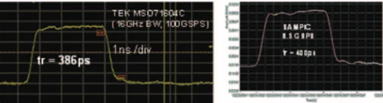
3.4.6. Bandwidth and signal quality. Signal bandwidth cannot be measured with sine waves because of the high-frequency currents then continuously flowing in the chip. Therefore, fast pulses are used instead. Figure 15 shows the similarity of the signal shapes recorded with both a 16 GHz/100 GS/s oscilloscope and SAMPIC at 8.5 GS/s. Hence we can extract a bandwidth for SAMPIC sitting well above 1 GHz. Cross-talk on the neighbouring channels is of the order of 2% and below 1% for the other channels, with a derivative shape of negative polarity.
Fig. 15. – Fast pulse recording: comparison between a 16 GHz/100 GS/s oscilloscope and SAMPIC. Left: Tektronix MSO71604C. Right: SAMPIC.
Fig. 16. – Blue: t-timing distribution without any timing correction 18 ps rms. Red: t-timing distribution after TINL correction 3.5 ps rms.
3.5. Time performances. –
3.5.1. Time resolution. In order to estimate the resolution of the time measurement, we use a high-end generator and split the signal to end up with 2 pulses like those shown in fig. 16 (450 mV, 800 ps risetime, 2 ns FWHM). After non-linearity and pedestal common correction, the timing for each pulse is calculated online using a digital CFD algorithm and interpolation as described in [8] or [9]. The time differences distributions measured in these conditions are shown in fig. 17. Without any time correction, we already get 18 ps RMS for Time Difference Resolution (TDR), which is already at the level of the best (calibrated and corrected) TDC and sufficient for a lot of applications. We know from previous work that this non-Gaussian distribution is mainly due to the spread of the delays (also called Time Integral Non-Linearity, or TINL) in the DLL and that it can be easily calibrated and reliably corrected. For this purpose, we have used the method we developed in 2009 [9] using the amplitude of segments of a sinewave crossing its mid-scale that permits a very fast calibration procedure. Once the TINL correction is applied, the TDR is reduced to 3.5 ps rms. Looking at the plots, on which all events are plotted, one can notice that there is neither tail in the distributions, nor hit out of time due to metastabilities, also no problem of boundaries between ranges, all of this validating the architecture of SAMPIC.
Fig. 17. – Left: time difference resolution vs. delay (set by cables). Right: TDR measurement between two SAMPIC chips (4.5 ps rms).
Fig. 18. – Measured time difference and TDR vs. input hit rate (left), and delay (right).
3.5.2. Time measurement as a function of the delay and the rate. The dependency of the TDR on the delay has been studied using two setups. To generate small delays we introduce a cable between the splitter and one of SAMPICs input. For larger cable delays, this method is no more usable, as the amplitude of the delayed signal diminishes and its risetime increases, both effect affecting the TDR. As shown in fig. 17, the latter first slightly increases before reaching a plateau. This feature can be easily explained since, for the very short delays, the two pulses are mostly recorded during the same DLL cycle. For delays larger than one clock period (i.e., 10 ns for 6.4 GS/s), they are captured during different DLL cycles, so that the jitters from the clock and the DLL are now added. For intermediate values the probability to record the two pulses within two different DLL cycles is proportional to the delay explaining consequently the progressive increase of the resolution. As shown in fig. 17, similar results are obtained using two SAMPIC chips from different mezzanines. In this case, as the two chips do not share the same DLL, the timing measurements on the two pulses are uncorrelated but the resolution remains better than 3.5 ps rms (4.5/√2). As shown in fig. 18, neither the input rate nor the delay between pulses affect the quality of the timing measurement, event for rates of few MHz. The independence to the delay is due to the fact that the virtual frequency multiplication is not based on a PLL but on a DLL fed by the main clock.
For large delays we repeat the test using signals provided by two channels of a Tektronix AFG 3252 [10] Arbitrary Waveform Generator (AWG). The 800 mV, 2.5 ns risetime, 4 ns FWHM, test pulses are slower than the previous ones but can be delayed digitally up to 10 us. As shown in fig. 18, the measured TDR is constant and better than 10 ps rms over the whole measurement range. This corresponds to 1 ppm of the full range and is far better than the 100 ps jitter specified for the AWG. Moreover, on the whole 10 us delay range, the difference between the programmed and measured delays is within +/−15 ps (+/−1.5 ppm), better than the precision specified for the AWG and showing a structure probably due to the AWG internal design. When the time calibration is performed in standalone mode (from internal sources), the ultimate time resolution is degraded by only 20%, which has no impact for most applications.
3.5.3. Time precision as a function of the amplitude. The TDR variation as function of the pulse amplitude and risetime is plotted in fig. 19. For this measurement, a 2 ns FWHM pulse is attenuated before being split towards two SAMPIC channels. Two kinds of attenuator, with different bandwidths have been used providing pulses with risetimes of respectively 500 and 800 ps. The measurements (symbols) are within very good agreement with the theoretical expectation.
Fig. 19. – Variation of TDR with the amplitude of the pulses for two different risetimes. The symbols are for measurements, the lines are corresponding to a fit using the quadratic sum model.
For both attenuators, the measured TDR is better than 15 ps rms for amplitudes larger than 100 mV and with the faster one a TDR better than 20 ps rms is already reached for pulses as small as 40 mV.
3.6. TOT measurement and filter . – SAMPIC houses an integrated Time-Over-Threshold (TOT) measurement. This is required since the time window is limited to 64 samples and one may want to get information about the total width of the sig-nal. Therefore, a 65th cell is implemented in each channel and devoted to the TOT. This ramp-based TDC has an adjustable range and permits measuring pulses between 2 ns and 1 us with a precision of 0.3% (see fig. 20). The TOT can also directly be used by the channel trigger to filter the events, which permits a potential powerful noise re-jection capability (this feature has been developed together with C.Williams@CERN for the SAMPET project).
3.7. Summary of functionalities. – SAMPIC is a full system on chip, which just requires power, clock, and a simple interface with an FPGA. Its main features and performances are summarized in fig. 21.
It can deal with analog or digital input, and performs the full digitization of the information. All the DACs and calibration generators are integrated. The very fast
Fig. 21. – Summary of SAMPIC performances.
and parallel conversion however remains the main limitation for dead-time. Dealing, for instance, with the number of bits of the conversion is a way to adapt its duration to the hit rate requirement. Figure 22 shows the effect of the number of bits used for the conversion on the Time Difference Resolution (TDR). For instance, a TDR of 10 ps rms can be reached with pulses of 50 mV converted over 8 bits. Input dead time can also be drastically decreased to a few ns by using the so-called Ping-Pong mode: in this case, the same input signal can be alternatively recorded in two consecutive channels. This permits recording close double hits, but obviously divides by two the number of physical channels. Like a standard TDC, the Waveform TDC is natively self-triggered on each of its channels. This may produce very large hit rates, which may cause a saturation of the output buffers, especially since the waveforms have to be extracted (partially or in totality) together with the time information. In order to reduce the dataflow, it is necessary to filter the good events before conversion. The central trigger located in the ASIC can then help defining trigger conditions and drastically reducing the hit rate. Moreover, adequate signals are provided in order to permit handshaking with the FPGA and performing a second level trigger based on smarter detector conditions, thus
Fig. 22. – Time difference resolution [ps rms] vs. amplitude as measured with the SAMPIC Waveform TDC.
or high energy physics, TOF-PETs). A slower version is under study for nuclear physics with sampling rates between 200 MS/s and 1 GS/s.
3.8. Status of development . – The first prototype of SAMPIC was submitted in the IBM 0.18 um CMOS technology and delivered in June 2013. Different upgrades and bug corrections have been performed since and the technology was moved to AMS 0.18 um. The latter was stopped end of 2018, and the design has now been migrated to TSI 0.18 um. A new version of the chip will be submitted to the MPW run of June 2020.
3.9. Taking data with detectors. – SAMPIC modules are already used with numerous detectors on test benches or test beams. A lot of examples were already presented at the WaveCatcher and SAMPIC Workshop in February 2018 in Orsay [11] (a second workshop is planned). The modules have been used with PMTs, MCP-PMTs, APDs, SiPMs, fast silicon detectors, diamonds: the performances are equivalent to those obtained with high-end oscilloscopes. Different R&Ds are ongoing with the TOF-PET community (CERN, IRFU [12, 13], USA) Many experiments have already used SAMPIC or intend to: CMS/TOTEM (on the LHC) [14], SHiP (SAMPIC is the baseline readout option for the Fast Timing Detector, the Surround Background Tagger and the Muon Detector) [15], LiquidO (R&D on new particle detector concept), T2K upgrade (Timing Detector) [15], Photek company (characterization of new ultra-fast MCP-PMTs [16]), Kansas University (satellites test benches at NASA), etc.
4. – Conclusion
In conclusion, signal waveform sampling permits access to a lot of information, but fast timing means large analog signal bandwidth and high sampling rates but this implies huge dataflow levels. The problem is to keep only the good information. In the case of high-end oscilloscopes, trigger is performed on digital data thus the use of fast ADCs is mandatory. Moreover, all types of calculation can be performed online on the data flow. But their cost limits their use to a few channels. Standard analog memories nicely replace ADCs in most cases, but dead-time remains their main limitation at high rates. This is not the case of TDCs but they do not provide the signal waveform. The Waveform TDC seems to be an adequate compromise in front of all these constraints.
The electronics chain of a TOF-PET scanner clearly resembles that of a particle physics detector. This is natural since the scanner is a cylindrical gamma photon detector where one looks for precisely determining the geographical origin of the two photons. The main difference sits in the destination of the recorded data and the way they are interpreted.
The main challenges when developing electronics systems for ps level measurement can be finally summarized as follows:
has to be avoided if possible.
• High rejection of wrong or noisy events via effective trigger configurations.
The Waveform TDC concept appears to be a very good candidate for addressing all these challenges, and to nicely fit the requirements of front-end electronics for a TOF-PET scanner.
∗ ∗ ∗
The author wishes to thank H. Grabas and O. Lemaire for their contribution to the ASIC design.
REFERENCES
[1] Genat J.-F., Varner G., Tang F. and Frisch H. J., Nucl. Instrum. Methods A, 607 (2009) 387.
[2] Perktold L. and Christiansen J., J. Instrum., 9 (2014) C01060.
[3] Vandenbroucke J., Bechtol K., Funk S., Okumura A., Tajima H. and Varner G.,
Development of an ASIC for Dual Mirror Telescopes of the Cherenkov Telescope Array,
arXiv:1110.4692 (2011).
[4] Ritt S., Design and performance of the 6 GHz waveform digitizing chip DRS4, in 2008
IEEE Nuclear Science Symposium Conference Record (IEEE) 2008.
[5] Breton D., Delagnes E., Maalmi J. and Rusquart P., The WaveCatcher family of
SCA-based 12-bit 3.2-GS/s fast digitizers, in 2014 19th IEEE-NPSS Real Time Conference
(IEEE) 2014, https://doi.org10.1109/RTC.2014.7097545.
[6] Delagnes E., Breton D., Grabas H., Maalmi J. and Rusquart P., Nucl. Instrum.
Methods Phys. Res. Sect. A, 787 (2015) 245249.
[7] Breton D., DeCacqueray V., Delagnes E., Grabas H., Maalmi J., Minafra N., Royon C.and Saimpert M., Nucl. Instrum. Methods Phys. Res. A, 835 (2016) 5160. [8] Delagnes E., What is the theoretical time precision achievable using a CFD Algorithm?
arXiv:1606.05541 (2016).
[9] Breton D. et al., Picosecond time measurement using ultra-fast analog memories, in
Proceedings of TWEPP-09, Paris, France (CERN) 2009, p. 149.
[10] Stricker-Shaver D., Ritt S. and Pichler B.J., IEEE Trans. Nucl. Sci., 61 (2014) 36073617.
[11] Maalmi J. and Breton D., WASIW-2018: WaveCatcher And SAMPIC International
Workshop, February 7–8 2018, LAL Orsay, France, http://wpsist.lal.in2p3.fr/
wasiw2018/.
[12] Canot C. et al., J. Instrum., 14 (2019) 12001.
[13] Yvon D. et al., Ultra-Fast Read-Out Trough Transmission Lines for TOF PET detectors
and ClearMind Project, Poster at IEEE-NSS 2019; N-19-102 (#1325).
[14] Bossini E., Instruments, 2 (2018) 21.
[15] Korzenev A. et al., JPS Conf. Proc., 27 (2019) 011005.
[16] Conneely T. et al., Multi-anode MCP-PMT Characterisation with high-channel count