Alma Mater Studiorum · Universit`
a di Bologna
Scuola di Scienze Corso di Laurea in Fisica
PHOTO-CURRENT SPECTROSCOPY
IN TIPS PENTACENE
SINGLE CRYSTALS
Relatore:
Prof. Beatrice Fraboni
Correlatore :
Dott. Laura Basiric´
o
Presentata da:
Alessandro James
Mirabelli
Sessione II
Abstract
Goal of this thesis is the study of the ultraviolet-visible photocurrent response in TIPS Pentacene single crystals, but also a description of the experimental method used to reach said objective. Emphasize is put on the approach utilized that this work imposed on us because of the challenges that arose. After preparing our organic semiconductor crystals, with the deposition of metal electrodes, our first measurement revealed that our initial experimental apparatus was not ideal to study the energy levels of a OSC, due to the slow and weak photocurrent response that many organic semiconductors have. A LabView program was therefore de-veloped in order to aid us in the construction of the photocurrent spectrum of our TIPS Pentacene single crystals.
Abstract
Obiettivo di questa tesi `e lo studio di uno spettro di fotocorrente nel range ultra-violetto visibile in cristalli singoli di TIPS Pentacene, ma anche una descrzione del metodo sperimentale utilizzato per raggiungere tale scopo. Per via delle difficolt`a incontrate durante il lavoro, viene messo in evidenzia il tipo di approccio usato. Dopo aver preparato i nostri cristalli di semiconduttori organici, con la deposizione di elettrodi metallici, la nostra prima misura ha rivelato che l’apparato sperimen-tale non era ideale per studiare i livelli energetici di un OSC; questo per via di un segnale di risposta di fotocorrente lento e debole proprio di molti semicondut-tori organici. Viene sviluppato quindi un programma LabView per costruire uno spettro di fotocorrente di cristalli singoli di TIPS Pentacene.
Introduction
Organic semiconductors (OSC) are a promise in the field of electronics due to their low fabrication costs and their versatility in finding new applications. In fact, the works of Alan J. Heeger, Alan G. McDiarmid and Hideki Shirakawa in the 70s, for which they were awarded the Nobel Prize in Chemistry in the year 2000 for the discovery and development of conductive polymers [1], opened the way for great innovation in electronics in the last 40 years. Semiconductors based on the Carbon atom can be chemically modified to obtain certain desired properties and more importantly they are compatible with organic tissue making them great candidates to enter the medical area of commercial application. Another well known everyday application can be found in the organic light emetting diodes (OLEDs) that are widely utilized for the fabrication of flexible displays.
Nowadays research focuses mostly on giving a solid explanation of the charge transport mechanism that govern transport properties of the OSC since a unified theory has not been declared yet. All this while finding new processes that allow the easy growth of single crystals. These being the ideal aggregation form on which to study the energy levels and intrinsic characteristics of organic materials [8].
In this thesis we first give a general outline of organic semiconductors: their physical properties and the characteristics of the material used in this project being the triisopropylsilylethynyl -pentacene (TIPS Pentacene). Next we explain some the most common OSC growth techniques with their pros and cons. We also provide the physical theory behind the electrical conductivity in organic material describing some of the models proposed for charge transport and photocurrent generation. In chapter 2 we describe all the procedures utilized to prepare our device to be ready for photocurrent measurement and the different experimental apparatus used to obtain said measure. Lastly we present our gathered data along side and analysis of the various challenges faced in order to reach the goal of this project, which is to obtain a photocurrent spectrum for TIPS Pentacene single crystals. We present the problems encountered along the way and the reasoning behind every solution adopted, and a description of the software program used to automatically analyze our gathered data.
Contents
1 Organic Semiconductors 1
1.1 General Properties . . . 1
1.2 TIPS Pentacene . . . 3
1.3 OSC Growth Techniques . . . 5
1.4 Charge Transport . . . 9 1.5 Photoconductivity . . . 11 2 Experimental Methods 15 2.1 Device preparation . . . 15 2.2 Experimental Setup . . . 17 3 Results 21 3.1 Data Acquisition . . . 22 3.2 Data Analysis . . . 28 3.3 LabView Program . . . 30 4 Conclusions 33 References 33 vii
Chapter 1
Organic Semiconductors
1.1
General Properties
Organic semiconductors (OSC) revolve around the Carbon element as the founding brick for all bigger and more complex structures that are known today. Other elements such as Hydrogen, Oxygen and Nitrogen are also present in different proportions and in different kinds of chemical bonds with Carbon, depending on the type of material and its structure. The magic of the Carbon element comes from its electronic configuration (1s2 2s22p2) with the 2s and 2p energy levels that
serve as valence states meaning that these are responsible for any chemical bonds with other atoms or molecules. An interesting property of this element is that when forming a bond with another atom, the orbitals involved are not only those residing in the single valence state, but often a combination of the two occurs. This happens because the energy difference between levels 2s and 2p of carbon is lower than the interaction energy between the orbitals that would form the bond. Therefore the creation of new energy levels, meaning new orbitals, by promotion of an electron from the 2s to 2p state, has a positive outcome in terms of energy gain when we consider what is released from the created bonds. The results are sp3, sp2 and sp hybrid orbitals (as shown in figure 1.1.[5]
(a) sp3
(b) sp2
Figure 1.1: Spatial disposition of sp3 (a) and sp2 (b) hybrid orbitals.
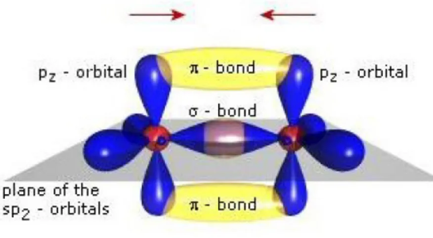
If we take two carbon atoms with sp2 hybrid orbitals (3 hybrid sp and 1 non
hybrid p orbital) one can identify two types of bonds: σ and π. The σ bonds are planar ones and they are located on the direction that directly connects two carbon nuclei. These are strong electronic bonds which allow little or no movement for the electrons. On the other hand, the π bonds are formed between the non hybrid pz orbitals that are located orthogonally to the nuclei plane (fig. 1.2).
Figure 1.2: The different σ and π bonds of the carbon atom.
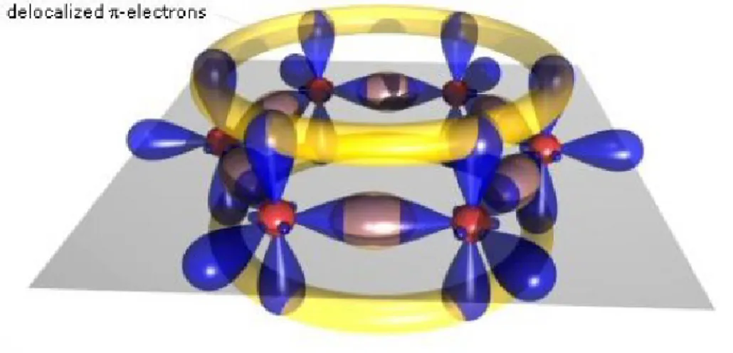
Consequently this kind of bond is weaker and allows more movement to the electrons involved. Todays research focuses more on multiple carbon atoms linked together. In this type of chain, the π bonds between atoms create an area of delocalized electrons (fig. 1.3), where they can move between atoms and molecules with a certain degree of freedom. These electrons, due to their high mobility, are
1.2. TIPS PENTACENE 3
the ones responsible for the electrical conductivity of the organic material as a whole.
Figure 1.3: The π bond chain, in yellow, where delocalized electrons can move.
In analogy with inorganic materials, it is possible to represent the energy levels of a molecule and identify the well known gap that distinguishes semiconductors from insulatorss and conductors, for organic ones as well. This energetic jump is situated between the HOMO (Highest Occupied Molecular Orbital) and the LUMO (Lowest Unoccupied Molecular Orbital) and the electrons involved come from the π bond. These can easily be excited from one level to the other since most organic semiconductors have the energy gap in the visible range (from 1,5 eV to 3,5 eV) thus requiring small amounts of energy. One should note the presence of internal energy levels in the HOMO-LUMO gap of organic semiconductors, absent in the inorganic counterparts. A refined energy structure is responsible of the different ranges of light absorption and the consequent variety of color that these materials can have. [11]
1.2
TIPS Pentacene
The material studied in this project was TIPS Pentacene 6,13-bis (triisopropylsilylethynyl-pentacene) (fig. 1.4).
Figure 1.4: Chemical structure of TIPS Pentacene [4].
Normal pentacene is an organic semiconductor (C22H14) composed of five linked
benzene rings (C6H6) in a planar structure. This carbon aggregate boasts the
high-est performances in terms of stability and measured mobilities (up to 3cm2/V s) though in its crystalline form, the resulting packing order, called herringbone [4],[8], (fig. 1.5), presents low π-π stacking which confers poor electron dispersion
Figure 1.5: Typical pentacene herringbone stacking motif [4].
in the solid structure. This means that pentacene transport capability is hindered by its crystal packing forming. To compensate this problem various derivatives have been synthesized by means of substitution or addition of chemical groups. It is possible to control and apply precise interventions, chemically speaking, to create many kinds of organic semiconductors[16].
Among these byproducts developed, our TIPS pentacene produced encouraging results in its use as thin film transistor[16]. The 6,13-bis triisopropylsilylethynyl-substituted pentacene presents two TIPS (C11H10Si) chemical groups connected
to the carbon atoms in position 6 and 13 of the molecule. This kind of material has risen in popularity due to its high charge transport mobility which can be further enhanced through different techniques[8]. The methods used can be all applied in large scale production, making the TIPS Pentacene a valuable candidate for future mass produced electronic devices.
1.3. OSC GROWTH TECHNIQUES 5
1.3
OSC Growth Techniques
If we want to have a go and try to understand conductivity and charge transport mobility, then we want to be working on high quality single crystal structures: a research device with long range order, minor or absent presence of grain bound-aries, few or none defects, a nice identifiable geometric shape, flat surface. Single crystals provide the opportunity to delve deep and glimpse intrinsic properties that govern it’s conductivity and mobility rules of a particular material[8],[9]. By using a material in it’s best performing form, we can use the results obtained to set a goal for when we investigate other, more practical, applications.
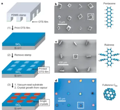
Researchers have proven that it is possible to effectively produce OSC sin-gle crystals in large arrays (fig. 1.6). By using octadecyltriethoxysilane (OTS) microcontact-printed domains onto clean Si/SiO2 surfaces, nucleation sites can
be controlled, and the effective crystal growth using vapour transport method can be achieved within 5 to 30 minutes, depending on the size of the array. One should note that any desired OTS pattern can easily be obtained with the help of a poly-dimethylsiloxane (PDMS) stamp with the appropriate relief structure. Small OTS square regions (5µm) have proven to support single discrete nucleation events, and the average temperature needed to obtain the OSC pentacene growth is ∼ 260 ℃. [3]
Figure 1.6: a) Schematic oultine of the procedure used to grow organic single crystals on substrates that have been patterned by microcontact painting. b) - d) Patterned single crystal arrays of variuos organic semiconductor material [3].
Another popular techinque utilized for crystal growth, is via saturated solvent solution[9]. Most organic materials are soluble in likewise organic solvents, such as toluene, benzene, chloroform and others; by creating a saturated solution of the desired crystal, and then pouring the liquid on a prefabricated substrate, crys-tallization can be achieved simply through solvent evaporation (fig. 1.7),which usually occurs at easily accessible temperatures [9].
Figure 1.7: In the solvent evaporation method, molecules crystallize due to increased concentration resulted from solvent evaporation [9].
One can refine this technique by using two solvents, in vapor or liquid state, with different dissolving degrees and a temperature sensible organic material: ap-plying precise temperature variations can induce a controlled crystallization per-centage in the desired device. This techinque is very popular at the moment and highly preferable because of it’s low cost and low temperature requirement. If we are ever to start using organic semiconductors in more day day applications, then of course we need to keep in mind the mass production/customization factor. If it is not economically favourable to grow single crystals in large scales, then we will always be confined to a research/study environment. The fact that also low temperatures are required, adds to the low cost benefit lists, since no expensive ma-chinery is necessary. The usage of plastic substrates is also allowed because of this last factor: higher temperatures would ruin/melt the substrate. Flexibility device also becomes an option which may facilitate the transition to more applicational purposes. [3]
A different method, mainly used to achieve a higher chemical purity, is physical vapor transport (PVT) [9][12]. Depending on the type of system (open, closed or semi-closed fig. 1.8), the organic material is first heated inside a growth tube and once sublimed, it flows to another area where it deposits and re-crystallizes. In an open or semi-closed system, the impurities, that posses a different molecular weight than the organic counterparts, flow away outside the tube leaving the newly crystalline device free from chemical defects and other unwanted molecules. It was seen that most organic compounds cannot undergo crystallization when under a high vacuum condition, or if they manage, the result is not a pretty one, with an amorphous crystal that does not meet the long range order desired. To fix this problem, inert gases, such as hydrogen, argon and nitrogen, are blown inside the
1.3. OSC GROWTH TECHNIQUES 7
Figure 1.8: PVT systems: open (a), closed (b) and sem-closed (c). Sublimation occurs in Zone 1 and Crystallization happens in Zone 2 [9].
growth tube and structural order can be achieved in the growing OSCs. The great advantage of this method is that molecular impurities are effectively separated and removed making PVT the growth procedure that has yielded the best results in terms of chemical purity, long range order, and electrical performance of single crystal devices.
In TIPS Pentacene the π-π stacking distance critically affects the charge car-rier mobility and it is set at fixed distance of 3.33˚A in both thin film and bulk crystals[6]. It is possible to intervene on the crystal lattice to induce strains to shorten the packing distance. This intervention has shown to increase the charge transfer integral, which describes the electronic wavefunction overlap between ad-jacent molecules. Several techniques have been developed to enhance the mate-rial’s conductivity, all of them involve the lowering of the important π-π stacking distance, known to be the key for higher mobility.
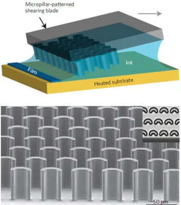
A limit at 3.08 Armstrong [6] has been reached since evidence has shown that intervening on shearing solution speed, a common method to induce strains in the crystal lattice, doesn’t always correspond to a higher mobility. Actually it has been found that by increasing this speed, after a certain point the number of grain boundaries created in the less oriented crystallites, become relevant and lower the material’s conductivity. A shearing technique that employs the aid of micro-pillars on the blade, allows for millimeter scale wide crystalline domains to form, and it is proven to significantly lower the number of grain boundaries (fig. 1.9).
Figure 1.9: A schematic of solution shearing using micropillar-patterned blade is shown in the top image. The ink containing the organic solution is spread onto the heated substrate. By changing the speed at which the blade moves, it is possible to alter the π-π stacking distance. For clarity the blades were not drawn to scale. The bottom image shows an electron scanning of the micropillar-patterned blade. The inset is a top view of the pillars from an optical microscope. The pillars are 35 µm wide and 42 µm high [16].
This method called FLUENCE (Fluid Enhanced Crystal Engineering) [16] has allowed to obtain record breaking results for charge hole mobility, along the shear-ing direction, at an average of 8.1cm2/V s with peaks at 11cm2/V s. These results can be attributed to the amount of control on the crystal solution growth and nucleation events that FLUENCE offers, while still being reproducible in many situations.
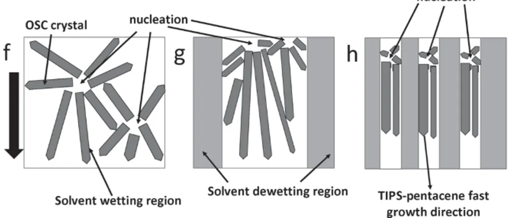
Another procedure uses lateral confinement of TIPS Pentacene to create lines of lattice strained and aligned crystals, by drawing a pattern on the substrate of alternate wetting/dewetting solvent areas[7] as shown in figure 1.10. The crystal is forced to grow from a nucleation site in a predefined direction, that of the shearing, which is also the favorable direction for electronic mobility. By reducing the width of the wetting lines, fewer nucleation events can occur in the same spot and more alignment is forced onto the growing single crystal domains though a limit has been found at 0.5um where otherwise the crystal would grow out onto dewetted
1.4. CHARGE TRANSPORT 9
areas as well. The results of this devices show an average of 1.68cm2/V s charge
carrier mobility and are amongst the highest for the short channel OTFTs that were later built and employed from these OSCs.
Figure 1.10: Diagram of the wetting/dewetting pattern. (f) shows how crystal growth is imagined: from a nucleation site, the crystal grows in the pointed direction. (g) and (h) show that by introducing dewetting regions (grey coloured), the decreased area where crystal growth is allowed (white coloured) forces these to become more aligned in the designated shearing direction (black arrow to the left) [7].
Single crystals are fundamental for the study of the organic semiconductors of which we still know little regarding charge transport and the general internal energy level structure. This needs to be emphasized. Only by researching this kind of aggregate, can we get a solid understanding of the internal structure and properties. Because of this, the goal is to always find new methods, or optimize of already existing ones, for high purity single crystal growth.
1.4
Charge Transport
When working with OSC we have to keep in mind that we don’t have a clear understanding of the intrinsic properties and the mechanisms that govern charge transport [15]. That is why experiments on highly crystalline ordered structures, such as the one conducted in this thesis, are crucial and critical for the determi-nation of conduction properties and the upper limits that carrier mobilities could reach.
Mobility (µ) [13] is a physical measurable quantity that is defined as a charged particle’s ability to move inside a medium in response to an external electric field. A material’s conductivity is closely related to its µ value, and for organic ones, we usually find values between 10−5 and 10cmV s2, while the inorganic cousins can
reach up to 103 cm2
V s [13]. To aid the theory and reach a better understanding
of how mobility works inside organic crystals, several models have been used. The first one comes from the study of the inorganic counterparts, of which we have more precise knowledge, and that is the band like transport : highly ordered molecules in a crystal structure with well defined electronic states and overlapping orbitals that create electronic bands. That would be the case of an inorganic device, but for an organic one things may vary. For a starter we have conjugated carbon molecules and their array of p orbitals that can degenerate thus creating splitting and delocalization. So even in the constituents of what will later be the crystalline system, we can recognize a certain kind of bandgap system: between the already mentioned HOMO (Highest Occupied Molecular Orbital) and LUMO (Lowest Unoccupied Molecular Orbital).
Another difference is the bonding that keeps together the crystal as a whole: organic molecules are bound with one another via the weak Van der Waals interac-tions. It is therefore possible to view the formation of the system as a perturbation of the original molecular electronic levels, which can be identified in a shift of the HOMO and LUMO levels by amounts of the order of 1 eV, to bring a decrease in bandgap width when forming a crystal. The existence of electronic bands is not a sufficient condition for charge transport to actually occur via a band like model. As it happens, in organic crystals, molecular relaxation occurs when external charges are introduced and it greatly affects the conductivity of devices made from these materials. A criteria to ensure that charge transport can take place with a certain bandwith W, is: [13]
W > h/tvib (1.1)
where tvib is the characteristic vibration time and h is the reduced Plank’s
constant. With this simple formula we are sure that a charge leaves a molecule before geometrical relaxation and self trapping can take place. Average bandwidth values that allow band transport are around 0, 1 and 0, 2 eV [13].
Mobility in an ideal crystal structure should only be hindered by thermally induced vibrations of the crystalline lattice. In a system where the molecules are so tightly bonded together, the perturbation of a single brick causes small movement in the whole structure. With higher temperatures, the possibility of an acoustical phonon scattering, the quasi-particle connected to thermal induced lattice vibrations, increases and therefore decreases the carrier mean free path, which leads to lower overall mobility. For a band like transport model, mobility is shown to be proportional to T32, but only at low temperatures ( < 100k), whereas
for increasing values of T, it drops significantly as: [13]
µ = T−a, a < 0 (1.2) This is basically what happens in inorganic semiconductors, but for organic
1.5. PHOTOCONDUCTIVITY 11
ones, this model is not sufficient because the overlapping molecular orbitals instead of creating extended conduction bands over long range ordered structures, are more restrained and localized due to the amount of disorder present. Localized states are those in which the charge carrier’s wavefunction has a nonzero amplitude in a finite region around a particular point, called localization site. The size of this region determines whether a state is weakly or highly localized, meaning a larger or smaller localization region. While studying charge transport in disordered materials it was found that the states were highly localized, meaning that carriers occupy a single site at a time and then ’hop’ to another, depending on spatial differences and energy levels. This also means, in accordance to what written above, that a charge carrier deforms the lattice around the site in which it is residing and during this time a polaron is formed, which is the embodiment of the electron-phonon coupling that is created when a polarized alteration occurs. This newly formed particle is what actually ’hops’ between the single localized states, since it is easily capable of overcoming the energy disparity that separates the states. Following this logic, it is easily concluded that in the ’hopping’ transport model, polaron movement is aided by increasing temperature, since it leads to more phonon scattering that can help in the charge carrier movement [15]. As a result of this model, mobility is correlated to T, to be more precise, to: [13]
µ = exp(−T−a1), a < 0 (1.3)
For organic crystals we can locate the energy gap between HOMO and LUMO levels as the highly densed region containing the localized single states. This is in accordance to a charge transport model developed later, called the Multiple Trapping and Release model (MTR) [13], which unified the previous two to create a theory that involved both transport mechanisms. For the MTR, charge carriers spend most of their time in localized states referred to as traps, and are then thermally promoted to higher energy extended states in which they are able to move via drift or diffusion, but are trapped again by another localized state. In this model as well, higher temperature is followed by higher mobility:[13]
µ = e−1T ) (1.4)
.
1.5
Photoconductivity
Photoconductivity is an opto-electronic phenomenon that modifies a material’s conductivity by means of absorption of incident radiation in the visible-UV range.
Charge carrier density is modified as a result and the semiconductor’s conduction properties vary consequently.
To easily comprehend this process we can imagine an incident photon that pos-sesses enough energy to overcome the characteristic gap of semiconductors; when this particle is absorbed, an electron-hole coupling is created in the conduction and valence bands respectively, increasing the material’s general conductivity [14]. In a doped semiconductor however, the photon is absorbed by the impurity atoms which then release an electron in the conduction band, even if the energy involved is smaller than that of the band gap. Also, if the incident photon matches the ion-ization energy of the impurity atoms, then extra electrons are produced to further increase photoconductivity.
When speaking of organic semiconductors though, we have to remember that charge carrier creation does not only take place between the HOMO and LUMO energy levels, but also in processes that involve the formation of excitons[14]: an excited state that consist of a bonded electron-hole coupling. This duo however, when formed, is electrically neutral and must be treated as one entity that can later dissociate to form two free charge carriers in their respective bands. That means that the energy necessary to create this excited state (around 0.5 1 eV), is less than the one needed to create separated carriers. It should be easy to notice that these excitons are able to move through the crystal lattice via the hopping transport model, jumping to nearby localized states in adjacent molecules. However as we said, this is still a globally neutral couple and measurable charge carrier generation only occurs when the electron manages to separate itself from the hole. The disassociation process can be activated thermally or through an external applied field. The carriers then proceed to move in the lattice, causing relaxation in the structure as explained in the previous section. Having covered several charge carrier generation methods, we can now look at a material’s conductivity in general which, for an insulators or a semiconductor, is given by the following relation: [14] σ = e ∗ (n ∗ µn + p ∗ µp) (1.5) where n and p are the number of electrons and hole respectively, and µn and µp their mobilities.
When such a device is exposed to an electromagnetic radiation with appropriate energy, that is an appropriate wavelength, the absorption of photons results in the creation of electron hole pairs, therefore modifying the values of n and p and the value of σ by certain amount:
σ + σδ = e ∗ [(n + nδ) ∗ µn + (p + pδ) ∗ µp] (1.6) and by using the current density formula J = σ ∗ E, where E is the electric field applied, we can now measure the increase in current as:
1.5. PHOTOCONDUCTIVITY 13
Where Jph is the photocurrent measured in the exposed semiconductor and it
is directly related to the light absorbed by the device. To further comprehend photoconductivity we must mention the average lifetime τ of the electron hole pairs (the excitons) that are formed during light absorption. τ is an important parameter because it is related to the amount of recombination processes that annihilates the electron hole couple thus reducing charge carrier density and hindering the material’s conductivity. We can rewrite the conductivity formula by assuming that when incident light hits a photoconductor , an f amount of electron hole pairs are formed:
f ∗ τ n = δn (1.8)
f ∗ τ p = δp (1.9)
Here τ n and τ p indicate the average lifetime of electrons and holes. Through simple substitution we rewrite a material’s conductivity increase as: [14]
σδ = f ∗ e ∗ (µn ∗ τ n) + (µp ∗ τ p) (1.10) In this way, the importance of charge carrier average lifetime in photoconduc-tivity is shown. Later in this paper, it will be shown that organic semiconductors react more to certain wavelengths of incident light, even by a considerable amount with disparities that involve jumps from pico to nano scales. This kind of reaction is a hint of the internal structure of the TIPS Pentacene but in general of all or-ganic single crystals. The transitions between the HOMO-LUMO levels, identified as the response peaks of the device, is a clear testament to the fact that a simple band like transport model is not enough to fully cover and explain charge mobility in OSCs.
Chapter 2
Experimental Methods
To study ultraviolet-visible induced photocurrent in semiconductor materials we examine the registered electric current, in relationship with the wavelength of the incident electromagnetic (E.M.) radiation. A wide range was used in this work, from near ultraviolet to near infrared: basically most of the visible spectrum. Before describing the instruments used and the experimental apparatus, we must first briefly describe the preparation that the TIPS Pentacene devices undergoed.
2.1
Device preparation
For this work, TIPS Pentacene single crystals were provided to us from the Uni-versity of Trieste. The crystals themselves came in all sorts of different shapes and sizes: some smaller, some larger, other with hollows inside. Ideally we wanted an OSC device without structural defects and were looking for something as homo-geneous as possible: rectangular in shape and with at least one smooth surface. Therefore and initial skim was made to eliminate right off the bat those crystals that certainly would not have aided us in our work. After that, several TIPS Pentacene devices were prepared at the same time and all with the same method. All our black boxes, so to speak, were positioned on separate microscope slides that were initially cleaned with acetone (C3H6O) and isopropyl alcohol to eliminate
any possible residue and attached firmly to them with silver epoxy paste. We then tape fixed a metallic wire transversally across our devices as a shadow mask in order to create a surface channel on the semiconductor. Next, by means of vacuum thermal deposition we obtained metal electrodes on our devices.
For the evaporation process, 150mg of gold was used (Franco Corradi ). The wire, 0.5mm in width, was cut into shorter pieces and then bent into the shape of a horseshoe. As one may imagine, the tiny boomerangs where cleaned in an acetone solution with the help of an ultrasound machine (Branson, Emerson Industries)
for 15 minutes. This type of instrument uses mechanical vibrations to remove dirt and residue. For the next step the gold wire pieces were placed onto a larger and cleaned tungsten filament.
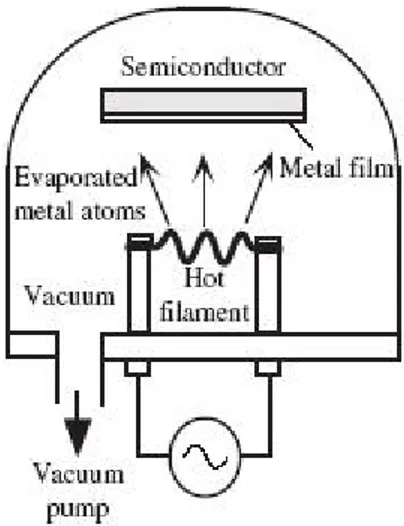
The filament itself is part of the machine that we used for vacuum thermal deposition (fig2.1).
Figure 2.1: Simple illustration of a vacuum thermal deposition machine
This bell shaped, glass case, contains a small platform and two poles inside. The tungsten filament is placed between the poles and the slides with the devices are situated below. With everything set, we then turned on the engine attached to the glass case and waited for it to reach an initial pressure of 10−2 Torr. After this, we let a 25A current pass through the poles in order to melt the gold wires just so that they turned into small droplets but making sure not to let them fall from the filament. Once the transformation was achieved, the current was returned to zero and the gold was left to cool down for 10 minutes. After all this preparation we then set the engine to reach a higher forced vacuum of 10−5 Torr, which took about around 2 hours. At the desired pressure, we once more let 25A of current pass through the filament and began the gold evaporation. At this stage, with the help of a magnet we moved the shutter, that was initially positioned above the TIPS devices to act as a shield. The gold, once evaporated, reaches the crystals and deposits itself on the surfaces thus creating the electrodes needed for the photocurrent measurements.
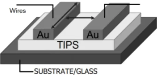
After no more gold droplets are left on the tungsten filament, the evaporation process is assumed to be terminated, and we can begin shutting down the machine. Once this long ordeal was over we then removed the metallic wire, revealing a 100µm wide conduction channel on the semiconductors , and connected thin gold wires to the gold electrodes, which in turn were joined to larger copper ones that
2.2. EXPERIMENTAL SETUP 17
allowed us to then implement the devices into our testing circuit. A simple diagram of the prepared DUT (Device Under Test) is shown in figure 2.2 while figures 2.3a and 2.3b show two evaporated TIPS.
2.2
Experimental Setup
To aid us in photocurrent measurements we were in need of some fundamental scientific equipment. First off, a reliable and stable source of E.M. radiation; an instrument that would be able to select and single out certain wavelengths of the aforementioned radiation; a device to read the current variation in our organic semiconductor; a piece of machinery to collect, read, and elaborate the data; an enclosed environment to keep our DUT shielded from any possible external and unwanted ambient radiation.
For this purpose we used a QTH (Quartz Tungsten Halogen, 150 W Roper Scientific TS 428S ) lamp set at 20V as our light source. Then, the incoming light passes through a slit, of adjustable width, and a mechanical chopper (Scitec Instruments, of adjustable frequency, before entering a monochromator (Spectra Pro 150 ) which possesses another slit. With this set-up, our DUT is subject to a continuous sequence of light and dark periods; all this while being irradiated by wavelength changing radiation.
Since we knew that the response signal was going to be low, we needed an instrument that would have been able to capture the small current and enhance it. This was done with the aid of a phase-sensitive lock-in amplifier (Stanford Research Systems SR530 ). This machine was synchronized with the chopper so that it captured and amplified only the current when the OSC was illuminated. After some initial tests though, we found out that we needed to change our experimental set up, the reasons of which will be explained later in chapter 4. For now it is sufficient to know that we swapped out the lock-in amplifier with an electrometer (Keithley 6517A figure 2.4). This time the electrometer was not connected to the chopper which was activated manually. Finally a LabView (National Instruments) program handled the plotting of the current values. The monochromator options
(a)
(b)
Figure 2.3: Images of two evaporated TIPS Pentacene taken with an OPTIKA micro-scope. Both of the conduction channels are about 100µm wide.
2.2. EXPERIMENTAL SETUP 19
such as wavelength range and step were settled from the software as well. A diagram of the experimental set up is shown in figure 2.5.
Figure 2.4: Image and technical specifications of the Keithley 6517A electrometer. [2]
Figure 2.5: Experimental set up used. In the first measurements, the lock-in amplifier was used instead of the electrometer and it was connected with the chopper [10].
The reason behind the use of such apparatus is because our DUT presents high resistivity, slow response, and very weak photosignal [10]. As explained in the previous chapters, in organic semiconductors, we have recombination processes that reduce the life time of charge carriers in the valence band and explain a weak response signal. To add to that, we have traps that can detain electrons for long time, hence slowing down the response signal. Therefore we needed a set up that could on one hand expose the TIPS for several seconds, allowing the crystal to reach saturation levels; and on the other hand, be able to repeat this process across a selectable range of wavelengths. The aim of this apparatus is to provide
and reveal the structural details of the organic semiconductor which would not be observed at higher frequencies. [10]
Chapter 3
Results
In this last chapter the experimental results are reported. We emphasize on the steps taken in the measurements and the issues encountered along the way. During all the measurements, the TIPS Pentacene single crystal was under 5V of electric potential and the QTH lamp was set at 20V . Both slits, the one near the lamp and the monochromator’s one, where set at 1mm in width. All our recorded photocurrent measurements where normalized with the photocurrent spectrum of the QTH lamp which is shown in 3.1 taken with a 300 - 800 nm wavelength range.
Figure 3.1: Photocurrent spectrum of the QTH lamp set at 20V and 300 - 800 nm range
3.1
Data Acquisition
Since we knew that TIPS Pentacene was a slow responding semiconductor to radi-ation, in the first set of measurements we set the chopper at the lowest frequency achievable by the instrument. We wanted to give the DUT as much time as pos-sible to reach current saturation levels when being illuminated, and disperse the current when in the dark. Therefore with the chopper set at 0.8Hz, the lowest frequency possible, we obtained a first photocurrent spectrum (fig. 3.2). The wavelength range used was 250 − 700 nm with a 2nm step.
Figure 3.2: Photocurrent measured with automatic chopper set at the lowest possible frequency (0.8Hz), and synchronized lock-in amplifier. The wavelength range was 250 − 700 nm and the step was 2nm.
Graph 3.2 was then normalized with 3.1, to obtain graph 3.3 which represents the photocurrent spectrum normalized with the incoming E.M radiation.
3.1. DATA ACQUISITION 23
Figure 3.3: Photocurrent measurement obtained with automatic chopper, normalized with the QTH lamp spectrum.
However, by looking at the results obtained, it was clear that something was not optimized in the measurement. The spectrum in graph 3.2 is not well-resolved, with gaps in the gathered data. We thought that it was just experimental noise, but after repeating the same measure, we concluded that it was not the case. This was our first challenge: we were not satisfied with the results.
We knew that TIPS Pentacene was a slow responding material so it needed more time for its photoresponse to reach saturation levels. As mentioned in chap-ter 3, it is common for organic semiconductors and polymers to have high resistivity and a slow response. Impurity atoms create defect states, that may act as recom-bination centers, hence reducing the amplitude of the response; and traps retain electrons, reducing the speed of the response. Thus, if the chopping frequency is too high, the material does not receive enough radiation during rise time. As seen in figure 3.4, imagine a common square modulation of radiation where till and tdar
are respectively the time when light is shining of the DUT, and when it is not. If till is sufficiently long, then our material can reach saturation level, and completely
discharge itself during tdar. On the other hand, if the duration of the illumination
period is shorter than the time required, then a steady state photocurrent (Iph) is
not reached. In this case the current decays and we loose information on the real photoresponse of the OSC. [10]
Figure 3.4: a) Illumination time is sufficient to obtain a steady state photocurrent. b) Il-lumination time is not long enough and the DUT cannot express all of its photoresponse, shown as the dashed curve [10].
The chopper could not be set at a slower frequency than what it was already at, so the only possible solution was to manually operate it and repeat the photocur-rent measurement. However, another apparatus change was necessary, one which was briefly mentioned in chapter 3: swap out the lock-in for the electrometer.
The lock-in worked only because it was synchronized with the chopper, now that the two were not connected anymore we had no need for it. That is why we opted for an electrometer which only had the duty to read constantly the photocurrent response and send that signal to a PC where the LabView program plotted all the values. From a conceptual point of view, we went back a step from where we were at the start of the experiment. The lock-in, in sync with the chopper, gave us data coming only from the light periods. This time though, with the electrometer, the machine and the LabView software reported the dark periods as well. Therefore we would later need to implement an extra step to compensate for this receding one.
In the first attempt with the new set up, the light/dark period was 30s long: 15s and 15s of illumination and dark. The wavelength range used was 350 − 750 nm with a 2nm step. The results are shown in graph 3.5 and 3.6.
3.1. DATA ACQUISITION 25
Figure 3.5: Photocurrent measurement with the manual chopper and the electrometer. Wavelength range employed was 350 − 750 nm with 2 nm as step.
Figure 3.7: Change of the shape of the photocurrent response signal as wavelength increases.
From graph 3.5 it can be noticed that from ∼ 480 to ∼ 530 nm the measured current is not in line with the rest of the values, as if our DUT had started to give a wrong response signal. Reasonably this was due to the fact that the organic semiconductor when exposed to a certain wavelength for a long period of time, over saturates and gives off wrong current readings. However, from graph 3.6 it is clear the continuous alternation between the phases where the TIPS Pentacene is illuminated and when it is not. One can easily spot where the light/dark phase ends or begins, just by looking at where the current starts to rise or decay. In figure 3.7, the change of the shape of the photocurrent curve can be appreciated: to the left, at lower wavelengths, the curve reaches saturation level as shown by the evident plateau; whereas to the right, at higher wavelengths, the shape changes becoming obviously bigger in amplitude but also sharper in it’s edges as to indicate that a saturated photocurrent is not reached.
It was clear that this measurement was not satisfactory: a considerable amount of data could no be accounted for while also being out of range with the rest of the values. Therefore we needed once again to repeat our measurement. This time we shortened the light/dark period to 20s : 10s and 10s, over a 300 - 700 nm wavelength range and 10nm step. The results are shown in graph 3.8 and 3.9.
3.1. DATA ACQUISITION 27
Figure 3.8: New photocurrent measurement. Again with manual chopper and electrom-eter. Wavelength range employed was 300 − 700 nm with 10 nm as step.
Figure 3.10: Detail of the change of the photocurrent curve.
The difference is evident. This time we have no weird or wrong readings during the measurement. The measure itself is less noisy. Graph 3.9 shows again the opposing periods of light and dark, that are evident by the sudden change of the photocurrent. Lastly in 3.10 we can see the change in shape of the curve, as the wavelength increases. It also noticeable the slight curve of the dark current in center area of the graph 3.8: this suggests that 10 s was not a sufficient time lapse for the TIPS to fully discharge itself.
3.2
Data Analysis
Now that we had a solid photocurrent set of data to start from, for our next step we needed to sort them. Out of the light and dark period, for our purpose, we only needed that section of data in which our DUT was illuminated by radiation. Therefore our first step was to analyze our acquired spectrum and separate what was needed from what was not. More specifically we only wanted the maximum current reached by the OSC during each period across all the wavelengths.
To achieve this we coded a program using the LabView (National Instruments) software. The Virtual Instrument (VI) was designed in order to read a data file of choice, be able to find photocurrent peaks in all illuminated periods and finally graph them. At the same time we also decided to map out manually the pho-tocurrent peaks from the same file. By doing this, the results of the LabView program would be validated: the manual graph would serve as a benchmark for
3.2. DATA ANALYSIS 29
us to compare the results obtained from the automatic mode and find eventual mistakes. The resulting outcome is shown in figures 3.11 and 3.12.
Figure 3.11: Graph of the light period current peaks obtained with the LabView soft-ware.
It is easy to see that the graphs are very similar in shape, meaning that the program developed to analyze the data works. As a final step, both of these graphs are normalized with the photocurrent spectrum of the QTH lamp from figure 3.1 to obtain graph 3.13
Figure 3.13: Comparison between the normalized photocurrent spectrums obtained from the two different procedures used.
The two spectra are almost identical apart from the first peaks. This differ-ence can be attributed to certain photocurrent peaks being different or completely missing in one of the analysis. But figure 3.13 clearly shows an overlapping of the slopes where the photocurrent starts to drop in value around the 500nm mark. The fact that both the curves have the same inclination, means in a definitive way that the program coded with LabView achieved our fixed goal.
3.3
LabView Program
We now briefly describe the development of the program used to read current peaks. An image of the front panel and the block diagram of the LabView program 3.14, 3.15.
The file of choice is read with the Read From Spreadsheet File function. This tool imports the data file and sorts out it’s content into a 2D, double precision
3.3. LABVIEW PROGRAM 31
Figure 3.14: Image of the front panel of the VI used.
array of numbers, strings or integers. Next we used the Delete From Array function to eliminate an initial segment of the arrayed data. This was needed because we did not have one unique switch to start all the instruments.
During the experiment, we first started recording data with a separate LabView program, with the OSC being in the dark, and only later we switched on the monochromator. Therefore a small lapse of initial zero values were always recorded. By eliminating these initial numbers we set our array to start from where the actual light/dark period begins.
Next step is using the Index Array Function to divide the array and analyze it. By doing this we create the time and current sub array. The time array goes onto the final output graph, but it is also used in the For Loop function, that we explain later. On the other hand, the photocurrent array is sent to the core function of the whole program: the Peak Detector VI. The name is self explanatory: the function takes a specified number of data samples in entry, which in our case is a single whole light period, and finds the highest value amongst them. Once found, the function returns the location of all the peaks in the block of data in entrance. The Peak Detector VI is based on an algorithm that fits a quadratic polynomial to sequential groups of data points. The number of points used in the fit depends on the number of data it receives in entry. It is possible to set a threshold to ignore undesired peaks or valleys. Since this function constantly reads a set number of data, if during the experiment measure, the chopper would have some sort of delay in changing position, then this would have an affect on all the following data read by the Peak Detector VI leading to eventual errors. The initial periods read would not match the ones read towards the end.
Figure 3.15: Block diagram of the VI used with the main functions indicated.
By using the Index Array Function again and the location index given by the Peak Detector VI it is possible to find the time and photocurrent values from the respective sub arrays. We use the For Loop to repeat this step until all the location values are processed. Once we have obtained all the photocurrent peak data and the time stamps, with the use of the Bundle Function we then associate the separate elements to create one cluster that is then graphed. We also graph the original entry data to compare the results obtained.
Chapter 4
Conclusions
With the development of the LabView program we were able to overcome the issues that derive in acquiring ultraviolet-visible photocurrent spectra of organic semiconducting single crystals, such as TIPS Pentacene. When materials have slow and weak signals due to the presence of traps and recombination centers as in this case, standard experimental setup for photocurrent spectroscopy could be inappropriate. If the organic material does not have time to reach saturation levels, then precious information is lost on its structure. Whereas a saturated photocurrent plateau could be clearly seen and appreciated in the second batch of measurements that were done after the change of experimental equipment. Giving more time to the TIPS Pentacene exposure to light allowed us to visualize its response during light and dark periods, and showing how it is harder for the organic material to reach that same saturated photocurrent at higher wavelengths where the change of the shape of the curve was also noticeable.
In this project we prove that even though being initially set back and having to measure both light and dark photocurrents with the electrometer, it is possible to find a valid solution to the limits presented by the slow response of the device. The solution comes under the form of a program able to analyze a alternating photocurrent signal from a molecular crystal and produce a spectrum that resulted being consistent with the one obtained via manual mode.
Bibliography
[1] http://nobelprize.org/nobel prizes/chemistry/laureates/2000/index.htm. [2] http://www3.imperial.ac.uk/pls/portallive/docs/1/7293199.pdf.
[3] Mang M. Ling-Shuhong Liu Ricky J. Tseng Colin Reese Mark E. Roberts Yang Yang-Fred Wudl & Zhenan Bao Alejandro L. Briseno, Stefan C. B. Mannsfeld. Patterning organic single-crystal transistor arrays. Nature, 444:913–917, 2006. [4] Laura Basiric´o. Inkjet Printing of Organic Transistor Devices. PhD thesis,
Univer-sity of Cagliari, 2012.
[5] Y. P. Bruice. Chimica Organica (4th edition). EdiSES, Napoli.
[6] Stefan C. B. Mannsfeld Sule Atahan-Evrenk Do Hwan Kim Sang Yoon Lee Hec-tor A. Becerril Al´an Aspuru-Guzik Michael F. Toney & Zhenan Bao Gaurav Gir, Eric Verploegen. Tuning charge transport in solution-sheared organic semiconduc-tors using lattice strain. Nature, 480:504–508, 2011.
[7] Michael Vosgueritchian Max Marcel Shulaker Gaurav Giri, Steve Park and Zhenan Bao. High-mobility, aligned crystalline domains of tips-pentacene with metastable polymorphs through lateral confinement of crystal growth. Advanced Materials, 26:487–493, 2014.
[8] Jeffrey B.-H. Tok Hanying Li, Gaurav Giri and Zhenan Bao. Toward high-mobility organic fieldeffect transistors: Control of molecular packing and large-area fabrica-tion of single-crystal-based devices. Material Research Society, 38:34–42, 2013. [9] Hui Jiang and Christian Kloc. Single-crystal growth of organic semiconductors.
Material Research Society, 38:28–33, 2013.
[10] N. V. Joshi. Photo-conductivity, Art, Science and Technology. Marcel Dekker Inc, 1990.
[11] J. Paula de P. Atkins. Physical-Chemistry (8th edition). Oxford U.P, 2006.
[12] Vitaly Podzorov. Organic single crystals: Addressing the fundamentals of organic electronics. Material Research Society, 38:15–24, 2013.
[13] Alberto Salleo Rodrigo Noriega. Organic Electronics II: More Materials and Appli-cations, Volume 2. Hagen Klauk,©Wiley, 2012.
[14] Alessandra Scid`a. Ion Implantation of Organic Thin Films and Electronic Devices. PhD thesis, University of Bologna, 2013.
[15] Yuanping Yi-Lingyun Zhu Veaceslav Coropceanu, Yuan Li and Jean-Luc Brdas. Intrinsic charge transport in single crystals of organic molecular semiconductors: A theoretical perspective. Material Research Society, 38:57–64, 2013.
[16] Gaurav Giri Jie Xu-Do Hwan Kim Hector A. Becerril Randall M. Stoltenberg Tae Hoon Lee-Gi Xue Stefan C. B. Mannsfeld Ying Diao, Benjamin C-K. Tee and Zhenan Bao. Solution coating of large-area organic semiconductor thin films with aligned single-crystalline domains. Nature Materials, 12:665–671, 2013.
![Figure 1.5: Typical pentacene herringbone stacking motif [4].](https://thumb-eu.123doks.com/thumbv2/123dokorg/7436190.99993/14.892.387.558.595.688/figure-typical-pentacene-herringbone-stacking-motif.webp)
![Figure 1.7: In the solvent evaporation method, molecules crystallize due to increased concentration resulted from solvent evaporation [9].](https://thumb-eu.123doks.com/thumbv2/123dokorg/7436190.99993/16.892.350.591.303.416/figure-evaporation-molecules-crystallize-increased-concentration-resulted-evaporation.webp)
![Figure 1.8: PVT systems: open (a), closed (b) and sem-closed (c). Sublimation occurs in Zone 1 and Crystallization happens in Zone 2 [9].](https://thumb-eu.123doks.com/thumbv2/123dokorg/7436190.99993/17.892.117.727.145.466/figure-systems-closed-closed-sublimation-occurs-crystallization-happens.webp)