Università degli Studi di Catania
Facoltà di Scienze Matematiche, Fisiche e Naturali
Dipartimento di Matematica e Informatica
Dottorato di ricerca in Matematica Applicata
XXV Ciclo
Optimization of homogeneous emitter and
thin-film solar cells
Angelo Greco
Advisor
Prof. Vittorio Romano
Optimization of homogeneous emitter and
thin-film solar cells
by
Angelo Greco
A thesis submitted in partial fulfillment for the degree of Doctor of Philosophy
at the Dipartimento di Matematica ed Informatica
"O frati," dissi, "che per cento milia perigli siete giunti a l'occidente,
a questa tanto picciola vigilia d'i nostri sensi ch'è del rimanente
non vogliate negar l'esperïenza, di retro al sol, del mondo sanza gente.
Considerate la vostra semenza: fatti non foste a viver come bruti, ma per seguir virtute e canoscenza".
Dante, Inferno, Canto XXVI, vv. 112-120
“Appena a sud del carbonio c'è il silicio. Come accade spesso tra i vicini si tratta di una prossimità ambigua, che crea un po' di disagio. Come il carbonio, ma in misura minore, il silicio ha la capacità di formare alcune tra le lunghe molecole a catena necessarie per i processi complessi come la vita. E tuttavia il silicio non ha dato origine a un proprio tipo di vita; forse però da questo punto di vista è solamente dormiente. I prodotti principali del carbonio, gli organismi viventi, hanno impiegato miliardi di anni per mettere a punto meccanismi di accumulo e dispersione dell'informazioni (una definizione austera e sintetica di ciò che intendiamo per «vita»); nel frattempo il silicio è rimasto in attesa. La recente alleanza tra le due regioni, che ha visto organismi basati sul carbonio sviluppare utensili basati sul silicio per la tecnologia dell'informazione, ha portato alla schiavizzazione del silicio. Però gli organismi basati sul carbonio sono ricchi d'inventiva e stanno sviluppando sempre più le potenzialità nascoste del silicio, tanto che forse un giorno il silicio capovolgerà i rapporti di forza con il suo vicino settentrionale e assumerà il ruolo dominante. Sicuramente sui tempi lunghi il silicio ha grandi potenzialità, perché il suo metabolismo e la sua replicazione possono essere meno complessi di quelli del carbonio. Questo potrebbe rivelarsi uno dei più astuti giochi di alleanze di tutto il Regno” […]
Peter Atkins, “The Periodic Kingdom: A Journey Into the Land of the Chemical Elements”. New York, BasicBooks, 1995
Acknowledgements ... i
Preface ... 2
1 Introduction to solar cells ... 4
1.1 Solar radiation ... 4
1.2 Silicon in photovoltaic technology... 6
1.3 Conduction band and valence band density of states and Fermi-Dirac distribution ... 8
1.4 Donors, acceptors and doped semiconductors ... 9
1.4.1 Drift and diffusion current ... 9
1.4.2 p-n junctions ... 10
1.5 Light absorption ... 12
1.5.1 Recombination ... 13
1.6 Theoretical limits to photovoltaic conversion ... 14
1.6.1 Recombination processes ... 15
1.6.2 Solar cells thickness ... 16
1.6.3 Light trapping coatings ... 16
2 Introduction to global optimization ... 16
2.1 Deterministic methods ... 16
2.2 Directions methods ... 19
2.3 Tunneling methods ... 20
2.4 Probabilistic methods ... 21
2.5 Simulated annealing methods ... 22
3 Introduction to multiobjective programming ... 24
3.1 Pareto optimality ... 24
3.2 Efficient and dominated points ... 26
3.3 Solution methods ... 28
4 Direct search algorithms for optimization calculations ... 35
4.1 Line search methods ... 35
4.2 Linear approximation methods ... 39
4.3 Quadratic approximation methods ... 45
5 Numerical simulation and modeling of monocrystalline selective emitter solar cells ... 50
5.2 Homogeneous emitter solar cell simulation ... 52
5.2.1 Selective emitter: dependence of efficiency on LDOP profile ... 52
5.2.2 Selective emitter: dependence of efficiency on HDOP profile ... 54
5.3 Analysis of loss mechanisms ... 55
5.4 Conclusions ... 56
6 Numerical simulation and modeling of rear point contact solar cells ... 57
6.1 Simulation setup ... 58
6.2 Physical models ... 58
6.2.1 Optical simulation ... 59
6.3 Results ... 59
6.3.1 Dependence of the output parameters on the metallization fraction ... 59
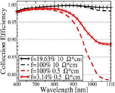
6.3.2 Collection efficiency of photo-generated carriers ... 62
6.4 Conclusions ... 63
7 Analysis and optimization of a homogeneous emitter solar cell ... 64
7.1 The tool employed: TCAD Sentaurus ... 64
7.2 Homogeneous emitter solar cell ... 64
7.3 TCAD/Optimization algorithm interface ... 65
7.3.1 Optimization algorithm ... 65
7.4 Results ... 66
8 Thin-film solar cells ... 69
8.1 Introduction ... 69
8.2 Optimization techniques ... 70
8.3 Anti Reflection Coating (ARC) ... 71
8.4 Texturing ... 73
8.5 Light trapping ... 74
9 Thin-film cells optical model ... 75
9.1 Multilayer thin-film structure ... 75
9.2 Parameters used in the simulation ... 76
9.3 Computation of the coherent absorption through the Matrix Method ... 77
9.4 Light’s diffused component evaluation through Monte Carlo method ... 79
9.5 Matlab simulation code ... 81
9.5.1 Input data and optical calibration ... 81
9.5.2 Computation of the absorbed radiance ... 81
9.5.3 Simulation and results ... 82
10.1 Introduction to Genetic Algorithms ... 92
10.2. GA theory in brief ... 92
10.3 The optimization problem ... 96
10.4 Mathematical formalization ... 96
10.5 Simulation and results ... 98
10.6 Results analysis ... 99
11 Multiobjective optimization for effective solar cell design ... 100
Introduction ... 100
11.1 The optimization algorithm ... 100
11.2 Sensitivity analysis ... 102 11.3 Robustness analysis ... 103 11.4 Identifiability analysis ... 103 11.5 Experimental results ... 105 Conclusions ... 107 References ... 108
i
Acknowledgements
First of all, I want to thank my advisor, Prof. Vittorio Romano, for his scientific competence, for his ability to teach and, above all, for his patience. Without his trust in me, I would not have ever begun my PhD studies.
Moreover, I would like to thank Prof. Giuseppe Nicosia, from the Dipartimento di Matematica e Informatica, Catania University, for all the scientific support he was willing to give me as for the Genetic Algorithm based Optimization part of this work.
Thanks also to Dr. Giovanni Carapezza, former Temporary Research Fellow at the Department, in cooperation with Prof. Nicosia.
I would like to remember that this thesis has been developed within the Project ENIAC Joint
Undertaking, Energy for a green society: from sustainable harvesting to smart distribution, equipment, materials, design solutions and their applications.
Finally, I thank my parents. They have always provided me with the moral support I needed when facing the tough challenge to complete my PhD studies while working as an engineer at the same time.
2
Preface
Over the last decades the world has been experimenting an increasing pressure to find solutions to energy crisis issues. As a result, the scientific research has been boosted towards the development of solutions related to alternative energy sources.
For the future decades, we can only imagine either to face the current standard energy demand or to face an increased one.
Since life quality levels are getting continuously better in most of the world, energy needs in such a scenario could be satisfied only by photovoltaic energy if we think to meaningfully cut the consumption of both traditional fossil fuels and nuclear energy.
This story comes from the past, the need for the development of renewable energy sources put itself under the world spotlight for the first time in the 70s, when the western countries experimented a serious energy crisis sponsored by the Middle-East OPEC countries that decided to dramatically reduce their crude oil export as a way to politically press over the western diplomacies after the Yom Kippur War between Israel and its Arab neighbors.
In the last twenty years, the Climate Change issues have gained enough popularity as well among developed countries’ public opinions to become a further motivation to invest in the research and development of renewable sources in order to improve their efficiency.
In this geopolitical context, several research programs have been supported. Among them, the
ENIAC Project Joint Undertaking, Energy for a green society: from sustainable harvesting to smart distribution, equipment, materials, design solutions and their applications, within which the present
work has been performed.
In particular, this thesis is focused on the optimization of photovoltaic cells, through the use of mathematics tools and optimization techniques based on new theories like the Genetic Algorithm ones.
In the first chapter, the solar cell physics is briefly introduced, with special attention to light absorption phenomenon, to the main sources of loss in photovoltaic conversion and to the most important geometric parameters involving the cell efficiency, that will be the object of the analysis in the following chapters.
In the second chapter, the global optimization problem and main techniques are introduced: the deterministic methods, the direction, the tunneling and the probabilistic methods, showing their advantages and drawbacks.
Since we will usually deal with more than one objective function to optimize in our analysis, the multiobjective programming techniques are introduced in the third chapter, taking into account Pareto optimality theory and the most important multiobjective techniques, ranging from the ex-ante to the ex-post methods, to the interactive ones, suggesting to us the importance of the solver opinions in order to give importance to results and search directions.
In the fourth chapter, we deal the direct search algorithm for optimization, ranging from the line search methods, to the linear approximation to the quadratic approximation ones.
Then, in the fifth chapter, a numerical simulation of a monocrystalline selective emitter solar cell is presented. As for the model implementation, the tool used has been the Technology Computer Aided Design (TCAD) Sentaurus. Moreover, a homogeneous emitter cell is presented and simulated in the same section, taking into account the dependence of efficiency on both LDOP (lowly doped) and HDOP (heavily doped) profiles. Finally, it has been performed an analysis of the loss
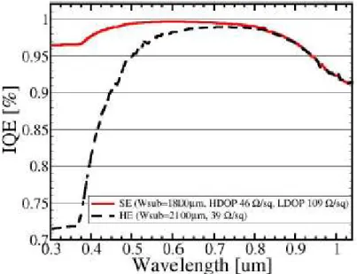
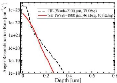
3 mechanisms involving the photovoltaic cells, bounding the Internal Quantic Efficiency of both HE (Homogeneous Emitter) and SE (Selective Emitter) cells, getting to the conclusions of the advantages of the SE cell over the HE one.
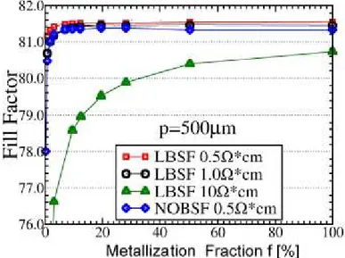
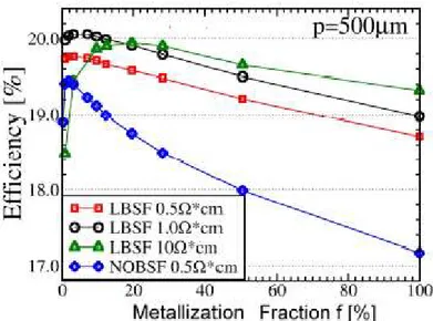
Anyway, also the number and the way the contacts are placed within the cell play a key role in optimizing the device’s efficiency. That is why in the sixth chapter, it has been performed a simulation of a rear contacted solar cell with special attention to the dependence of the cell’s output on the metallization fraction as for the short circuit current, the fill factor, the open circuit voltage and the device’s internal efficiency.
In the seventh chapter, a homogeneous emitter cell has been simulated, writing a Matlab input code to perform the simulation with given parameters by the TCAD Sentaurus. A genetic algorithm has been used, gaining an improvement in Fill Factor and Efficiency of the simulated cell with regard to the HE cell of the seventh chapter. Since we are trying to optimize both fill factor and efficiency of the device, we deal with a multiobjective problem and some trade-offs solutions have been introduced among the points of the Pareto front. The simulation has been launched twice, using a maximum number of generations of 300 and 1700 respectively. By the combined use of both a genetic algorithm and a such a powerful tool like TCAD Sentaurus, the results obtained in this part are innovative and represent a quantitative improvement of the results previously obtained over this argument in literature. The comparison against the reference structures, together with the improvements gained is summarized in the tables and figures at the end of the chapter.
In the eighth chapter, the thin-film cells are briefly introduced. Since the pressure towards the efficiency increase has got strong and stronger in last two decades, this gives a simultaneous answer to the increasing material and manufacturing cost of photovoltaic devices.
In the ninth chapter, the thin-film physics is briefly described, together with the mathematical methods that will be used in the following chapter to calculate the absorption and the light’s diffused component. So, this chapter is dedicated to the thin-film optical model, but it also deals with the Monte Carlo method, a powerful stochastic method that will be used to model in a stochastic way the photons behavior in the photovoltaic device.
In the tenth and last chapter, the thin-film silicon cell is optimized through the use of a Genetic Algorithm. Since the thin-film technology is intimately bound to the reduction of production costs, the optimization problem takes into account the balance between the thickness of the cell layers and the manufacturing cost, becoming a profit maximization problem. Also this chapter deals with the thin-film structures from an innovative standpoint. The obtained results are new and they represent a noticeable improvement in the optimization of a tandem cell.
4
1
Introduction to solar cells
Semiconductor solar cells are fundamentally quite simple devices. Semiconductors have the capacity to absorb light and to deliver a portion of the energy of the absorbed photons to carriers of electrical current – electrons and holes. A semiconductor diode separates and collects the carriers and conducts the generated electrical current preferentially in a specific direction. Thus, a solar cell is simply a semiconductor diode that has been carefully designed and constructed to efficiently absorb and convert light energy from the sun into electrical energy. [13]
A solar cell, so, is a device able to convert part of the energy coming from sunlight into electrical power, by the exploitation of the photovoltaic effect, that takes place when the light on a double leyer of semiconductive material produces a potential difference between the layers.
1.1 Solar radiation
All electromagnetic radiation, including sunlight, is composed of particles called photons, which carry specific amounts of energy determined by the spectral properties of their source. Photons also exhibit a wavelike character with the wavelength, λ, being related to the photon energy, Eλ, by the
equation [1]
𝐸= 𝑐
where h is Plank’s constant and c is the speed of light.
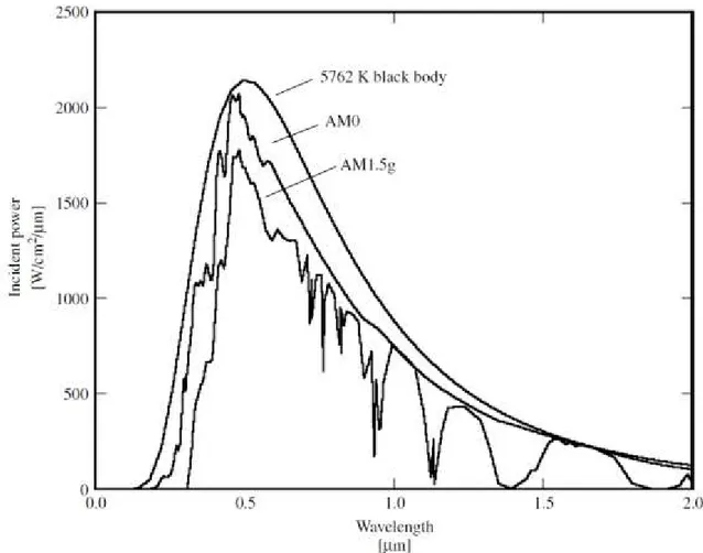
The sun has a surface temperature of 5762 K and its radiation spectrum can be approximated by a black-body radiator at that temperature. Emission of radiation from the sun, as with all black-body radiators, is isotropic. However, the Earth’s great distance from the sun means that only those photons emitted directly in the direction of the Earth contribute to the solar spectrum as observed from Earth. Therefore, for practical purposes, the light falling on the Earth can be thought of as parallel streams of photons. Just above the Earth’s atmosphere, the radiation intensity, or Solar Constant, is about 1.353 kW/m2 and the spectral distribution is referred to as an air mass zero (AM0) radiation spectrum. The Air Mass is a measure of how absorption in the atmosphere affects the spectral content and intensity of the solar radiation reaching the Earth’s surface. The Air Mass number is given by [2]
𝐴𝑖𝑟 𝑀𝑎𝑠𝑠 =𝑐𝑜𝑠1
where θ is the angle of incidence (θ = 0 when the sun is directly overhead). The Air Mass number is always greater than or equal to one at the Earth’s surface. An easy way to estimate the Air Mass has been given by Green as
𝐴𝑖𝑟 𝑀𝑎𝑠𝑠 = 1 + 𝑆 𝐻
2
where S is the length of a shadow cast by an object of height H. A widely used standard for comparing solar cell performance is the AM1.5 spectrum normalized to a total power density of 1 kW/m2. The spectral content of sunlight at the Earth’s surface also has a diffuse (indirect) component owing to scattering and reflection in the atmosphere and surrounding landscape and can account for up to 20% of the light incident on a solar cell. The Air Mass number is therefore further
__________________________________________________________________Introduction to solar cells
5 defined by whether or not the measured spectrum includes the diffuse component. An AM1.5g (global) spectrum includes the diffuse component, while an AM1.5d (direct) does not. [1]
Black body (T = 5762 K), AM0, and AM1.5g radiation spectrums are shown in the picture below
Figure 1.1 - The radiation spectrum for a black body at 5762 K, an AM0 spectrum, and an AM1.5 global spectrum
The specific amount of energy carried by photons is related to the spectral properties of the source they come from. Below, it is possible to get a look on the light spectrum, related to the wavelength.
6 As we have already seen when introducing the Air Mass parameters, the atmosphere is responsible for alterations of the electromegnatic spectrum. This is, essentially, due to two reasons. The first one is that the atmosphere is divided into different layers and each of them is responsible for the absorption of radiations with a specific wavelength. The second one is that the atmosphere is responsible for the phenomenon of the Rayleigh’s scattering, related to the collision among different light wavelength and the air, leading to a radiations’ alteration. [22]
1.2 Silicon in photovoltaic technology
Solar cells can be fabricated from a number of semiconductor materials, most commonly silicon (Si) – crystalline, polycrystalline, and amorphous. Materials are chosen largely on the basis of how well their absorption characteristics match the solar spectrum and their cost of fabrication. Silicon has been a common choice due to the fact that its absorption characteristics are a fairly good match to the solar spectrum, and silicon fabrication technology is well developed as a result of its pervasiveness in the semiconductor electronics industry. [21]
Electronic grade semiconductors are very pure crystalline materials. Their crystalline nature means that their atoms are aligned in a regular periodic array. This periodicity, coupled with the atomic properties of the component elements, is what gives semiconductors their very useful electronic properties. Below, you can see an abbreviated periodic table of elements.
Figure 1.3 – Part of the periodic table of elements
Note that silicon is in column IV, meaning that it has four valence electrons, that is, four electrons that can be shared with neighboring atoms to form covalent bonds with those neighbors.
In the case of Silicon, each atom forms a covalent bond with four more atoms, and these are all valence atoms. That is the way the lattice in the molecular structure of silicon is created. [18]
The dual behavior of semiconductor, insulant at low temperatures and conductive at higher ones, can be related to the behavior of electrons between valence and conduction bands. When temperature increases, the thermal energy somministrated to the lattice, leads to the breaking of some covalent bonds created among valence atoms. These atoms, thermally excited, can jump away from the valence band to the conduction band and they will be responsible for the conduction phenomena in photovoltaic.
The amount of energy needed to break this kind of bond is called band gap (Eg) and can be
determined as follows in the case of silicon [1]
__________________________________________________________________Introduction to solar cells
7 So, for a temperature of 0 K, the band gap for silicon is 1.21 eV, and, at room temperature (300 K), it has decreased to 1.1 eV. That is why, at temperatures below zero, semiconductors are usually considered as insulant materials. [22]
When temperature increases, the probability for a valence electron to break its covalent bonds and jump to the conduction band increases too. This phenomenon involves not only the valence electrons, because, when one of more of them leaves the valence band, it is no more completely occupied by the electrons, so, electrons belonging to lower states of the band can move to fill the free states in the valence band if properly excited by an electric camp.
A material with the previously underlined features is called intrinsic semiconductor. In this case, the density of electrons is equal to the density of holes. [1]
As shown in the picture below, electron near the maxima in valence band have been thermally excited to the empty states near the conduction-band minima, leaving behind holes. The excited electrons and remaining holes are the negative and positive mobile charges that give semiconductors their unique transport properties.
Figure 1.4 – A simplified energy band diagram at T > 0 K for a direct band gap (EG) semiconductor. Electrons near the maxima in valence band have been thermally excited to the empty states near the conduction-band minima, leaving
behind holes. The excited electrons and remaining holes are the negative and positive mobile charges that give semiconductors their unique transport properties
8
1.3 Conduction band and valence band density of states and Fermi-Dirac distribution
The dynamic behavior of the electron can be established from the electron wave function, ψ, which is obtained by solving the time-independent Schrodinger equation:
∇2 +2𝑚
2 𝐸 − 𝑈(𝑟) = 0
where m is electron mass, h is the reduced Planck constant, E is the energy of the electron, and U(r) is the periodic potential energy inside the semiconductor. This equation states that the electron energy is quantized. If we consider a wave function (r) and a sample made up by a cube of material through which r is the position vector, the huge number of energy levels allowed for the electron is very close one to another. [2]
So, if we consider the energy interval (E, E+dE), the number of states that own this level of energy is indicated as n(E)dE, with n(E) indicated as density of allowed states.
𝑛 𝐸 =8 2𝜋𝑚
3/2𝐸1/2
3
Not all of the allowed states are occupied. The density of occupied states will be 𝑛0 𝐸 = 𝑛 𝐸 𝑝(𝐸)
With 𝑝(𝐸) called Fermi-Dirac function of probability. It expresses the probability that a state at a given energy would be occupied as well.
𝑝 𝐸 = 1
𝑒 𝐸−𝐸𝐹 /𝑘𝑇 + 1
Where EF is the Fermi’s energy, the energy at which we have p=1/2, k is the Boltzmann’s constant
and T is the absolute temperature. This equation suggests that the parameter with a real importance is E-EF that is the difference between the energy of the considered electron and the Fermi’s energy, because only the electrons with an amount of energy close to the Fermi’s one can play a role in the electrical conduction process. [25]
In the picture below, you can see the Fermi’s energy at various temperatures. [2]
__________________________________________________________________Introduction to solar cells
9
1.4 Donors, acceptors and doped semiconductors
Because of their low density, intrinsic semiconductors cannot produce a sufficient current for normal applications. Anyway, it is possible to alterate the normal properties of these materials through an adequate increase of carriers by doping the materials. Doping, in electronics, consists in contaminating the semiconductor with special impurities.
Let us consider a crystal of pure silicon, where we insert some atoms of elements of the 5th group, like phosphorus. Four electrons belonging to these atoms will be shared with the closest silicon atoms to create covalent bonds, while the fifth electron, still available for an additional bond, will stay with its phosphorus atom. So, the thermal excite and the following jump to the conduction band would result easier for this last electron, rather for the others, now part of four covalent bonds. As a result, an energy of only 0.05 eV, will be enough to free this electron and make it available for the electrical conduction, while it would be necessary an energy of 1.1 eV to take a silicon atom electron from the valence band to the conduction one. [28]
The phosphorus atom, within the silicon lattice, is called donor, because it lends an electron to the conduction band. So, adding donor atoms, it is possible to increase the electron density within the conduction band.
Semiconductors doped with donor atoms are called ―n type‖ semiconductors, where n stands for negative, because the negative carriers (electrons) are much more than holes (positive carriers). In this type of semiconductors, electrons within the conduction band are called majority carriers, while the holes in the valence band are called minority carriers.
Let us consider now a pure silicon crystal doped with impurities belonging to elements from the third group of the periodic table, such as boron. Each boron atom is surrounded by four silicon atoms, but boron has three valence electrons, so one more electron is needed to complete the external atomic configuration (8 valence electrons). With a very low energy level, 0.05 eV it is possible to take an electron away from a silicon-silicon bond to use it to complete the valence configuration. The boron atom is so called acceptor, because it easily takes an electron from the valence band. Adding acceptor atoms, it is possible to dramatically increase the holes density within the valence band.
A semiconductor rich in this kind of impurities (acceptors) shows at room temperature an excess of positive carriers and it is called ―p type semiconductor‖. In this last kind of semiconductors, majority carriers are the valence band holes, while the minority carriers are the conduction band electrons.
1.4.1 Drift and diffusion current
While the impurities are inserted in the semiconductor lattice, it is needed to understand how these carriers move inside the material. Electron speed without any electrical field can be estimated between 0 and vf (Fermi’s speed, the speed of an electron with a kinetic energy equal to the Fermi’s
one Ef). While, when applying an electrical field, electrons are accelerated, so that they have a small
speed increase in the field direction, but towards the opposite versus, because electrons have a negative carriers, so that [1]
𝐹 = −𝑒𝐸
Electrons responsible for the conduction are the only ones with a speed close to vf.
The parameter that measures the capacity of carriers to move freely within the material under an electrical field E is the following one
𝜇 =𝑣 𝐸
10 where v is the speed of the electrons in the direction opposite to the field’s one. The current density of the carriers is called drift current. It is related to the carrier movement due to the electrical field over the semiconductor.
The drift current densities for holes and electrons can be written as 𝐽𝑝𝑑𝑟𝑖𝑓𝑡 = 𝑞𝑝𝑣𝑑,𝑝 for holes 𝐽𝑛𝑑𝑟𝑖𝑓𝑡 = −𝑞𝑛𝑣𝑑,𝑛 for electrons
So, these currents depends on drift speed for holes and electrons, on the number of holes and electrons and, finally, on the electron’s carrier.
Moreover, Electrons and holes in semiconductors tend, as a result of their random thermal motion, to move (diffuse) from regions of high concentration to regions of low concentration.
Much like how the air in a balloon is distributed evenly within the volume of the balloon, carriers, in the absence of any external forces, will also tend to distribute themselves evenly. This process is called diffusion and the diffusion current densities are given by
𝐽𝑝𝑑𝑖𝑓𝑓 = −𝑝𝐷𝑝∇𝑝
𝐽𝑑𝑑𝑖𝑓𝑓 = 𝑞𝐷𝑛∇𝑛
So, the total current, for both holes and electrons, can be calculated as follows 𝐽𝑝 = 𝐽𝑝,𝑑𝑟𝑖𝑓𝑡 + 𝐽𝑝,𝑑𝑖𝑓𝑓
𝐽𝑛 = 𝐽𝑛,𝑑𝑟𝑖𝑓𝑡 + 𝐽𝑛,𝑑𝑖𝑓𝑓 1.4.2 p-n junctions
The development occurred to the photovoltaic technology started just from the studies over the p-n junction, elementary structure of the semiconductor devices physics. The p-n junction, essentially, is made up by a n-type and a p-type semiconductor put close one to another. When this two devices lay one along the other, the diffusion phenomenon has place, so that the holes move from the p-zone to the n-p-zone and the vice-versa happens for the electrons from the n-p-zone to the p-p-zone. This happens because of the distribution of holes and electrons in the semiconductor device that is not uniform, so that the diffusion current is generated. This phenomenon ends when the carriers are distributed uniformly. The diffusion of carriers, determines a region between the junction, called ―depletion region‖, where finding carriers it is not possible and it is possible to measure an electric field not equal to zero, caused by the presence of ionized doping atoms, that is not counterbalanced by the lack of carriers within the region. [3]
__________________________________________________________________Introduction to solar cells
11
Figure 1.6 Simple solar cell structure used to analyze the operation of a solar cell. Free carriers have diffused across the junction (x = 0) leaving a space-charge or depletion region practically devoid of any free or mobile charges. The fixed charges in the depletion region are due to ionized donors on the n-side and ionized acceptors on the p-side
The difference of potential between the p-type and the n-type semiconductor is called ―built-in potential‖, and it is equal to:
𝑉𝑏𝑖 =𝐾𝑇 𝑞 𝑙𝑛
𝑁𝑎𝑁𝑑 𝑛𝑖2
where Na and Nd are, respectively, the p-type and n-type impurities concentrations introduced
during the doping phase and ni is the density of electrons in the conduction band.
The potential and the electrical field of the junction can be calculated using the abrout change
approssimation. According to this equation, if we assume the density of spatial carriers in the p and n regions equal to, respectively −𝑞𝑁𝑎 and 𝑞𝑁𝑑 we will have that
𝑥𝑛𝑁𝑑 = 𝑥𝑝𝑁𝑎
where 𝑥𝑛 and 𝑥𝑝 are the width of the depletion regions in the n-type and p-type semiconductors. So, we can argue that, in equilibrium, in any point of the depletion region, the effect of the electrical field is counterbalanced by the effect of concentrations variation.
Now, we can consider the Poisson’s equation: 𝑑2𝑉 𝑑𝑥2 = − 𝜌 𝜀 = 𝑞𝑁𝑎 𝜀
where is the density of carrier. So, integrating two times this equation, and assuming the boundary condition that the potential and the electrical field would be equal to zero for 𝑥 = −𝑥𝑝 , we have
𝑉 =𝑞𝑁𝑎 𝜀 𝑥2 2 + 𝑥𝑝𝑥 + 𝑥𝑝2 2
and it is now possible to express the potential for both sides of the junction: 𝑉𝑝 =𝑞𝑁𝑎𝑥𝑝2
2𝜀 and 𝑉𝑛 = 𝑞𝑁𝑑𝑥𝑛2
2𝜀
So, if we sum this two values, we have the total value of the potential barrier on the junction. The depletion region width can be calculated, approximately, considering the zone moving carriers free. In fact, when the intrinsec Fermi’s level Ei is close to the real one Ef, n and p become almost
12 equal to each other. Assuming that Na and Nd would be constant in the respective zones (step
junction), the depletion region width W is equal to 𝑊 = 𝑥𝑝 + 𝑥𝑛
1.5 Light absorption
The creation of electron–hole pairs via the absorption of sunlight is fundamental to the operation of solar cells. The excitation of an electron directly from the valence band (which leaves a hole behind) to the conduction band is called fundamental absorption. [3]
Both the total energy and momentum of all particles involved in the absorption process must be conserved. Since the photon momentum, pλ = h/λ, is very small compared to the range of the crystal momentum, p = h/_, the photon absorption process must, for practical purposes, conserve the momentum of the electron.1 The absorption coefficient for a given photon energy, hν, is proportional to the probability, P12, of the transition of an electron from the initial state E1 to the
final state E2. So, the photon absorption process in a direct band semiconductor can be represented
as in picture below
Figure 1.6 – Valence and conduction band in a direct band semiconductor
where the incident photon has an energy E2-E1>EG.
Absorption results in creation of an electron-hole pair since a free electron is excited to the conduction band leaving a free hole in the valence band. [18]
While, in indirect band semiconductors, like silicon, where the valence-band maximum occurs at a different crystal momentum than the conduction-band minimum, conservation of electron momentum necessitates that the photon absorption process involve an additional particle. Phonons, the particle representation of lattice vibrations in the semiconductor, are suited to this process because they are low-energy particles with relatively high momentum. This phenomenon is represented in the following picture
__________________________________________________________________Introduction to solar cells
13
Figure 1.7 – Photon absorption in an indirect band gap semiconductor for a photon with energy hν < E2 − E1 and photon with energy hν > E2 − E1. Energy and momentum in each case are conserved by the absorption and
emission of a phonon, respectively
Photon absorption in an indirect band gap semiconductor for a photon with energy h < E2 − E1 and a photon with energy h > E2 − E1. Energy and momentum in each case are conserved by the absorption and emission of a phonon, respectively.
In both direct band gap and indirect band gap materials, a number of photon absorption processes are involved, though the mechanisms described above are the dominant ones. A direct transition, without phonon assistance, is possible in indirect band gap materials if the photon energy is high enough. Conversely, in direct band gap materials, phonon-assisted absorption is also a possibility. 1.5.1 Recombination
When a semiconductor is taken out of thermal equilibrium, for instance by illumination and/or injection of current, the concentrations of electrons (n) and holes (p) tend to relax back toward their equilibrium values through a process called recombination in which an electron falls from the conduction band to the valence band, thereby eliminating a valence-band hole. There are several recombination mechanisms important to the operation of solar cells – recombination through traps (defects) in the forbidden gap, radiative (band-to-band) recombination, and Auger recombination. The net recombination rate per unit volume per second through a single level trap (SLT) located at energy E = ET within the forbidden gap, also commonly referred to as Shockley–Read–Hall recombination, is given by 𝑅𝑆𝐿𝑇 = 𝑝𝑛 − 𝑛𝑖 2 𝜏𝑆𝐿𝑇,𝑛 𝑝 + 𝑛𝑖𝑒𝐸𝑖𝑘𝑇−𝐸𝑇 + 𝜏𝑆𝐿𝑇,𝑝 𝑛 + 𝑛𝑖𝑒 𝐸𝑇−𝐸𝑖 𝑘𝑇
where the carrier lifetimes 𝜏𝑆𝐿𝑇 are given by
𝜏𝑆𝐿𝑇 =
1 𝜍𝜈𝑡𝑁𝑇
Where 𝜍 is the capture cross section, vth is the thermal velocity of the carriers, and NT is the
14 to a carrier traveling through the semiconductor at velocity vth. Small lifetimes correspond to high
rates of recombination. If a trap presents a large target to the carrier, the recombination rate will be high (low carrier lifetime). When the velocity of the carrier is high, it has more opportunity within a given time period to encounter a trap and the carrier lifetime is low. Finally, the probability of interaction with a trap increases as the concentration of traps increases and the carrier lifetime is therefore inversely proportional to the trap concentration. [25]
Radiative (band-to-band) recombination is simply the inverse of the optical generation process and is much more efficient in direct band gap semiconductors than in indirect band gap semiconductors. When radiative recombination occurs, the energy of the electron is given to an emitted photon – this is how semiconductor lasers and light emitting diodes (LEDs) operate.
Auger recombination is somewhat similar to radiative recombination, except that the energy of transition is given to another carrier (in either the conduction band or the valence band). This electron (or hole) then relaxes thermally (releasing its excess energy and momentum to phonons). Just as radiative recombination is the inverse process to optical absorption, Auger recombination is the inverse process to impact ionization, where an energetic electron collides with a crystal atom, breaking the bond and creating an electron–hole pair.
Interfaces between two dissimilar materials, such as, those that occur at the front surface of a solar cell, have a high concentration defect due to the abrupt termination of the crystal lattice. These manifest themselves as a continuum of traps within the forbidden gap at the surface; electrons and holes can recombine through them just as with bulk traps. Rather than giving a recombination rate per unit volume per second, surface traps give a recombination rate per unit area per second. A general expression for surface recombination is
𝑝𝑛 − 𝑛𝑖2 𝑝 + 𝑛𝑖𝑒𝐸𝑖𝑘𝑇−𝐸𝑡 𝑆𝑛 + 𝑛 + 𝑛𝑖𝑒𝐸𝑖𝑘𝑇−𝐸𝑡 𝑆𝑝 𝐷Π(𝐸𝑡) 𝐸𝑐 𝐸𝑣 𝑑𝐸𝑡
where Et is the trap energy, D(Et) is the surface state concentration (the concentration of traps is
probably dependent on the trap energy), and Sn and Sp are surface recombination velocities.
1.6 Theoretical limits to photovoltaic conversion
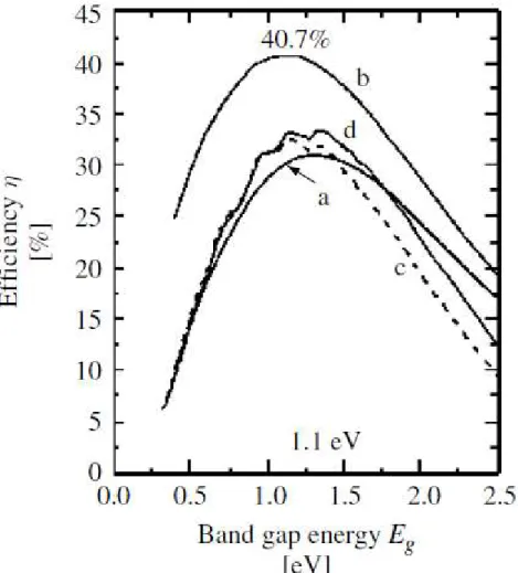
The conversion efficiency, maybe, is the most important parameter in photovoltaic tehcnology. The sun energy density is not as low as we cannot expect a generalized use of its energy, but, simultaneously, it is not so high that we can consider its exploitation simple. L’efficienza di conversione è forse il parametro più importante della tecnologia fotovoltaica. [14] La densità energetica del sole non è tanto bassa da non permetterci di avere aspettative su un uso generalizzato e efficiente della sua energia, ma, al tempo stesso, non è così alta da rendere ciò semplice. The solar cells efficiency is closely related to the hole-electron pairs due to the insulation and to the possibilità to avoid their recombination before they are conveyed into the outlet electrical circuit at evaluated the maximum efficiency to be expected from the solar cells, at 40.7% for the photonic spectrum approximated by the black body at the temperature of 6000K. [15] This value is not too high if we consider that the solar cells performs a inefficient use of photons, because most of them are not absorbed and their energy is not exploited in an optimal way. [1]
__________________________________________________________________Introduction to solar cells
15 1.6.1 Recombination processes
Photons are absorbed in order to get conveyed towards the conduction band from the valence band, according the process known as electron-hole pair generation. Anyway, the same process can take place in the opposite versus, when an electron comes back to its valence band. As a result, the difference between the electrons pushed towards the conduction band by the sunlight absorption and the electrons that fall again into their valence band is equal to the net current extracted from the solar cell. This statement can also be presented as an equation [1]
𝐼
𝑞= 𝑁𝑠 − 𝑁𝑟 = 𝑛𝑠 − 𝑛𝑟
∞ 𝜀𝑔
𝑑𝜀
where g represents the band gap, while Ns and Nr are the inlet and outlet photons flows into and
from the solar cell respectively, through any surface. In other words, if the cell is adequately contact equipped, the current is made up by the electrons that leave the conduction band through the n-type contacts, adequately doped. In the same way, in the valence band, the I/q ratio, represents the electrons that enter the valence band through the highly doped p-type contacts.
Finally, it is possible to estimate the solar cell theoretical reachable efficiency, as a function of the band gap, according to Shockley and Quesisser’s assumptions, at 40.7%.
16 1.6.2 Solar cells thickness
If we consider the electrical perfomance, the optimal thickness depends on materials’ structure and quality and it can involves several aspects. The thinnest cells can absorb less light, but this drawback can be counterbalanced by light trapping technologies. Moreover, the losses due to the shadow side of the device can decrease when reducing the cell thickness. It is also to be taken into account the economic pressure, from an industrial standpoint, towards the decrease of cell thickness, in order to reduce the product material costs, since a thinner cell is simply made up by less silicon.
1.6.3 Light trapping coatings
Silicon is featured by an high reflection index. It has been calculated that, when it is not coated, silicon reflects 30% of incident radiation. This is the way reflection losses are generated. A widely used solution, consists in the use of a material with a very low reflection index as a coating for silicon. This coating is generally an insulant material, designed to reduce reflection. Industrial trends are now positioned on the use of Titanium oxides through the process of chemical vapour
deposition (CVD). [1]
2 Introduction to global optimization
Given a function 𝑓: 𝐼𝑅𝑛 → 𝐼𝑅, the global optimization methods tries to determine the global minum
of the function 𝑓(𝑥), that is a point 𝑥∗ in such a way that: [5]
𝑓 𝑥∗ ≤ 𝑓 𝑥 ∀ 𝑥 ∈ ℝ𝑛
These methods can be divided into the following groups: 1. Deterministic methods
2. Methods for Lipschitzian functions 3. Directions method
4. Tunneling methods 5. Probabilistic methods
2.1 Deterministic methods
A function 𝑓: 𝐼𝑅𝑛 → 𝐼𝑅 is called Lipschitzian if there exists a constant L > 0 (called Lipschitz’s
constant) exists in such a way that for any 𝑥1, 𝑥2 ∈ ℝ𝑛 it holds [41]
|𝑓 𝑥1 − 𝑓 𝑥2 | ≤ 𝐿||𝑥1− 𝑥2||
In other words a Lipschitzian function satisfyies the following statements: 𝑓 𝑥 ≥ 𝑓 𝑥0 − 𝐿 𝑥 − 𝑥0
𝑓 𝑥 ≤ 𝑓 𝑥0 + 𝐿| 𝑥 − 𝑥0 |
__________________________________________________________Introduction to global optimization
17 The following function 𝑓 𝑥 is a Lipschitzian one
Figure 2.1 – A Lipschitzian function
The algorithms belonging to this group of optimization methods have in common the research for the value that minimizes the following problem:
min
𝑥∈𝐼𝑛
𝑓(𝑥) with 𝐼𝑛 = 𝑥: 𝐴𝑖 ≤ 𝑥𝑖 ≤ 𝐵𝑖 ∀ 𝑖 = 1,2, … , 𝑛
We assume that:
1. The n-dimensional cube 𝐼𝑛 should be in such a way that it contains a global minimum for
𝑓(𝑥)
2. The function would be Lipschitizian over 𝐼𝑛
3. The L Lipschitz’s constant would be known or it would be known its overestimation 𝐿 One of the most popular algorithm among these methods is the Schumbert-Mladineo’s one. [41] First step. Let it be 𝐿 > 𝐿; given 𝑥0 it is defined the function
𝐹0 𝑥 = 𝑓 𝑥0 − 𝐿 | 𝑥 − 𝑥0 | and 𝑥1 is chosen so that:
𝐹0(𝑥1) = min
𝑥∈𝐼𝑛 𝐹0 𝑥
kth step. Once you get 𝑥𝑘 the following function is defined 𝐹𝑘 𝑥 = max
𝑗 =0,…,𝑘 𝑓 𝑥𝑗 − 𝐿 ||𝑥 − 𝑥𝑗||
18 𝐹𝑘 𝑥𝑘 + 1 = min𝑥∈𝐼
𝑛
𝐹𝑘(𝑥)
the function 𝐹𝑘 𝑥 is featured by a very particular structure that can be used to define algorithms that in a finite number of steps solve the problem
min
𝑥∈𝐼𝑛
𝐹𝑘(𝑥) So, if 𝑓∗ is the minimum value of 𝑓(𝑥) over 𝐼
𝑛, let they be 𝐹𝑘∗ the minimum values of 𝐹𝑘(𝑥) over
𝐼𝑛. Let it be Φ ≡ 𝑥∗ ∈ 𝐼
𝑛, 𝑓 𝑥∗ = 𝑓∗ and let it be 𝑥𝑘 the sequence of points generated by the
previous algorithm, then, it follows: lim 𝑘→∞𝑥inf∗∈Φ| 𝑥 ∗− 𝑥 𝑘 | = 0 lim 𝑘→∞𝑓 𝑥𝑘 = 𝑓 ∗
and that the sequence 𝐹𝑘∗ is not decreasing and
lim
𝑘→∞𝐹𝑘 ∗ = 𝑓∗
Method’s benefits
1. It does not require the solver to calculate the derivatives
2. It is possible to determine the point’s sequence 𝑥𝑘 convergence, both from a theoretical and a computational standpoint
3. A stopping criterion exists for the algorithm. If 𝑥𝑘 and 𝐹𝑘∗ are the sequences generated,
you have the following ones:
𝑓 𝑥𝑘 ≥ 𝑓∗ ≥ 𝐹 𝑘∗
𝑓 𝑥𝑘 ≥ 𝑓∗ ≥ 𝑓 𝑥
𝑘 + 𝑟𝑘
where 𝑟𝑘 = 𝐹𝑘∗− 𝑓 𝑥
𝑘 and lim𝑘→∞𝑟𝑘 = 0 because of the previous theorem. So, if 𝑟𝑘 <
then 𝑥𝑘 is a minimum for 𝑓(𝑥) , far away from it for only an . Method’s drawbacks
1. it can be very difficult to define, ex-ante, an n-dimensional cube 𝐼𝑛 containing at least a global minimum of 𝑓(𝑥)
2. the method can be very heavy, from a computational point of view, because of the computing of 𝐹𝑘(𝑥) at each step
3. the hypothesis that 𝑓(𝑥) would be a Lipschitzian function is very restrictive 4. it is not always possible to get an overestimation of the Lipschitz’s constant
__________________________________________________________Introduction to global optimization
19
2.2 Directions methods
The basis idea of the directions method is to define some directions, containing all the local optimals and to choose, among them, the one related to the lowest value of the objective function. These methods have been firstly proposed in the 70s, without getting good results at that time. Lately, through the implementation of a new, general approach, these methods have come again under the spotlight. The most popular direction method is the Branin’s method. [42]
Branin’s method
Let us suppose that 𝑓(𝑥) is continuous and ∇𝑓(𝑥) would be continuous as well. If you choose an 𝑥0 it is possible to define some directions 𝑥(𝑡) in which ∇𝑓(𝑥 𝑡 ) is parallel to ∇𝑓(𝑥0). So, through the solution of the following system
𝑑
𝑑𝑡 ∇𝑓 𝑥 𝑡 = ±∇𝑓 𝑥 𝑡
assuming the initial condition 𝑥 0 = 𝑥0 it is possible to get some directions satisfying the following one
∇𝑓 𝑥 𝑡 = ∇𝑓(𝑥0)𝑒±𝑡 The Branin’s method is based on the following steps:
1. Determination of the solution 𝑥 𝑡 of the system 𝑑
𝑑𝑡 ∇𝑓 𝑥 𝑡 = −∇𝑓 𝑥 𝑡 , 𝑥 0 = 𝑥0
2. the direction 𝑥 𝑡 allows us to determine a stationary point 𝑥∗ di 𝑓(𝑥). In fact, since
lim
𝑡→∞∇𝑓 𝑥 𝑡 = lim𝑡→∞∇𝑓 𝑥0 𝑒
−𝑡 = 0
the direction 𝑥 𝑡 tends to 𝑥∗.
3. the stationary point 𝑥∗ is slightly perturbated, gaining to the point 𝑥
0 = 𝑥∗+ 𝜀 and the
following system is solved 𝑑
𝑑𝑡 ∇𝑓 𝑥 𝑡 = ∇𝑓 𝑥 𝑡 , 𝑥 0 = 𝑥 0 gaining the direction 𝑥 𝑡 .
4. along the direction 𝑥 𝑡 we get away from the stationary point 𝑥∗ because the norm of the
gradient increases as 𝑡 increases:
20 so, the direction 𝑥 𝑡 is followed until 𝑡 , when 𝑥 𝑡 is out of the stationary point ―attraction zone‖.
5. the following system is now solved again 𝑑
𝑑𝑡 ∇𝑓 𝑥 𝑡 = ∇
2𝑓 𝑥 𝑡 𝑑𝑥 𝑡
𝑑𝑡 = ∇𝑓(𝑥 𝑡 )
and the result is 𝑑(𝑥 𝑡 )
𝑑𝑡 = ±∇
2𝑓 𝑥 𝑡 −1∇𝑓(𝑥 𝑡 )
these last equations define a Newton-like method. Because the Hessian matrix can become singular, the previous equations can lose meaning for some 𝑡. If 𝐴(𝑥) is the adjoint matrix of ∇2𝑓(𝑥), 𝐴(𝑥)
always exists and it is true that ∇2𝑓(𝑥)−1 = 𝐴(𝑥)
det [𝛻2𝑓 𝑥 ] , so, the previous system can be replaced
through a new parameterization with the following system 𝑑𝑥 𝑡
𝑑𝑡 = ±𝐴 𝑥 𝑡 ∇𝑓 𝑥 𝑡 Comments on the Brainin’s method [42]
It has never been proved that this method would be globally convergent, that is the curve defined reaches the global minimum.
If the method is convergent, it is hard to know how many stationary points 𝑓(𝑥) has and, because of it, it is hard to state a stop criterion for the algorithm.
The direction 𝑥 𝑡 is attracted by all the 𝑓(𝑥)’s stationary points.
The numerical solution of the differential equation systems defining the curve 𝑥 𝑡 is heavy from a computational standpoint.
2.3 Tunneling methods
The tunneling methods have been proposed in order to find in an efficient way the global minimum for functions with many local minima (in cases where the previous direction methods would not be adequate).
Tunneling algorithms’ structure
Tunneling algorithms are made up by a sequence of cycles, each cycle is made up by two steps: a minimization phase, during which the objective function is minimized and a tunneling phase, where a ―good‖ starting point is got for a following minimization phase.
Minimization phase
Given a starting point 𝑥0, a local search is performed. It is equivalent to apply any convergent algorithm to a local minimum 𝑥0∗.
Tunneling phase
The solver efforts are to find a point 𝑥1 ≠ 𝑥0 in such a way that
__________________________________________________________Introduction to global optimization
21 so, theoretically, the tunneling methods generate a sequence in such a way that
𝑓 𝑥𝑘∗ ≥ 𝑓 𝑥𝑘+1∗
and that the 𝑥𝑘 points come close to the global minimum ―passing under‖ the less important local minima, without taking into account how many and where they are.
This last feature is very important for problems with a lot of minima. The main drawback of these methods are the difficulties met when trying to find an x in such a way that 𝑓 𝑥 = 𝑓(𝑥𝑘∗) and
𝑥 ≠ 𝑥𝑘∗. In order to avoid this situation, a new point is found, by the zero of the following:
𝑇 𝑥, 𝑥𝑘∗ = 𝑓 𝑥 − 𝑓(𝑥𝑘
∗)
[(𝑥 − 𝑥𝑘∗)𝑇(𝑥 − 𝑥 𝑘∗)𝜆]
where is chosen iteratively, in such a way that the pole in 𝑥𝑘∗ introduced in 𝑇 𝑥, 𝑥
𝑘∗ makes
𝑓 𝑥 − 𝑓(𝑥𝑘∗) equal to zero. Moreover, it must be taken into account that this method has no stop criterion. In fact, we could look for an 𝑥 in such a way that 𝑓 𝑥 = 𝑓(𝑥𝑘∗), even when 𝑥
𝑘∗
is already the global minimum for 𝑓 𝑥 .
2.4 Probabilistic methods
The probabilistic approaches define the global optimization problem over a limited region 𝐷 ⊂ ℝ𝑛
that is:
min
𝑥∈𝐷𝑓(𝑥)
Among the different probabilistic methods, we can refer to: - Methods using random directions
- Multistart methods - Chichinadze’s methods - Simulated annealing methods Methods using random direction
When using this group of algorithms, at each iteration, the direction 𝑑𝑘 is chosen randomly over an n-dimension sphere, with a unitary radius. These methods are based on the Gaviano’s theorem, that states that if the sequence 𝑥𝑘 is in such a way that
𝑥𝑘+1 = 𝑥𝑘 + 𝛼𝑘𝑑𝑘
where 𝑑𝑘 is chosen randomly over the previous n-dimension sphere with a radius equal to 1 and 𝛼𝑘 so that:
𝑓 𝑥𝑘+ 𝛼𝑘𝑑𝑘 = min
22 then, 𝑓 𝑥𝑘 − 𝑓∗ < 𝜀 happens with a probability that tends to one.
Multistart methods
These methods are based on the following considerations. [43]
Let 𝑚(. ) be the Lebesgue’s measure over D. If A is a set with a measure m(A) in such a way that 1 ≥𝑚(𝐴)
𝑚(𝐷) = 𝛼 ≥ 0
the probability P(A,N) that, taking into account N points randomly extracted (over D), at least one is inside A is given by:
𝑃 𝐴, 𝑁 = 1 − (1 − 𝛼)𝑁 and, from this equation, it follows:
lim
𝑁→∞𝑃 𝐴, 𝑁 = 1
so, we can conclude that, if we choose randomly many points, one of them, almost surely, is very close to the global minimum 𝑥∗.
2.5 Simulated annealing methods
These methods take inspiration from quantic mechanics theories. Let us consider a system made up by a very large number of particles of the same kind and let s stands for the system state and E(s) energy associated to this state. [53]. If the system is in thermal equilibrium, then the probability density that it would be in the state s is proportional to
𝑒−𝐸(𝑠)𝐾𝑇
where, as defined in the previous chapters, K is the Boltzmann’s constant and T is the temperature. It is generally known that, when lowering the temperature, states with low energy increase their own probability, up to the limit, when the temperature reaches the absolute zero and the only possible states are the ones with zero energy.
Now, let us consider a system, that associates at each state x, an energy amount: 𝐸 𝑥 = 𝑓 𝑥 − 𝑓∗≥ 0
where, 𝑓∗ is the global minimum for 𝑓 𝑥 . Now, if the temperature would tend to zero, the states 𝑥∗
would become more likely, in such a way that:
𝐸 𝑥∗ = 𝑓 𝑥∗ − 𝑓∗ = 0
__________________________________________________________Introduction to global optimization
23 Let f(x) be a continuous function over a compact set D ⊂ ℝ𝑛. Let us assume that only one global
minimum x* exists for f(x) over D. Then, it is true that:
𝑥𝑖∗ = lim 𝑇→0 𝑥𝑖𝑒−(𝑓 𝑥 −𝑓 𝑥 ∗ )/𝑇 𝑑𝑥 𝑒−(𝑓 𝑥 −𝑓 𝑥∗ )/𝑇 𝑑𝑥 = lim𝑇→0 𝑥𝑖𝑒−𝑓(𝑥)/𝑇𝑑𝑥 𝑒−𝑓(𝑥)/𝑇𝑑𝑥 𝑖 = 1, … , 𝑛
that can be also expressed as:
𝑥𝑖∗= lim
𝑇→0 𝑥𝑖𝑃𝑇 𝑥 𝑑𝑥 = lim𝑇→0𝑥 𝑖 𝑇
where 𝑃𝑇 𝑥 = 𝑒−𝑓(𝑥 )/𝑇
𝑒−𝑓(𝑥 )/𝑇𝑑𝑥
it is a probability density where 𝑥 𝑖 𝑇 are the average values of some aleatory variables distributed according the density 𝑃𝑇 𝑥 .
Then, the basic idea of these optimization methods is to simulate some aleatory arrays distributed according the probability density 𝑃𝑇 𝑥 .
As T decreases, the arrays generated by the simulation come closer and closer, from a probabilistic standpoint, to the global minimum we are looking for.
The different algorithms belonging to this group, use different ways to perform this simulation.
Stop criteria
Within these probabilistic methods, a large number of different stop criteria have been proposed, but, the most interesting one is the one using a certain number of randomly chosen points over D, that tries to give to the solver an approximated value, as a probability 𝑃 𝑤 of the function
𝑃 𝑤 =𝑚( 𝑥: 𝑓 𝑥 ≤ 𝑤 ) 𝑚(𝐷)
where, as usual, m(.) is a set’s Lebesgue’s measure. After that, a point 𝑥∗ can be considered a good
estimation of the global minimum if
24
3 Introduction to multiobjective programming
An optimization problem can be defined as both the minimization or maximization of a real function over a specified set. [8]
Its importance derives from the evidence that many real issues are formulated as an optimization probem. Anyway, almost any optimization problem is featured by the simultaneous presence of different objectives, that are real functions to be minimized or maximized, usually in conflict one against another. [58]
Let us consider the following optimization multiobjective problem:
min (𝑓1(𝑥)𝑓2 𝑥 … 𝑓𝑘 𝑥 )𝑇 𝑤𝑖𝑡 𝑥 ∈ 𝐹 ⊆ ℝ𝑛 (1)
where 𝑘 ≥ 2 𝑎𝑛𝑑 𝑓𝑖:ℝ𝑛 → ℝ
𝐹 is the set of feasible decision variables.
From now on we will refer to ℝ𝑘 as the objective space and ℝ𝑛 as the decision variables space.
An array 𝑥 𝜖 ℝ𝑛 so will be a decision array while 𝑧 𝜖 ℝ𝑘 is an objective array.
We will refer, moreover, to 𝑓(𝑥) as the objective function array (𝑓1(𝑥)𝑓2 𝑥 … 𝑓𝑘 𝑥 )𝑇 and to
𝑍 = 𝑓 𝐹 = 𝑧𝜖ℝ𝑘: ∃𝑥 ∈ 𝐹, 𝑧 = 𝑓(𝑥)
as the imagine of the feasible region in the objective space
Especially, it is possible to say that an objective array 𝑧𝜖ℝ𝑘 is feasible when 𝑧 ∈ 𝑍.
Moreover, it is possible to define the ideal objective array 𝑧𝑖𝑑 as the array whose components are
𝑧𝑖𝑖𝑑 = min
𝑥∈𝐹 𝑓𝑖(𝑥)
The ideal situation represents the simultaneous optimization of all the objective functions. If there would not be conflicts among them, the trivial solution would be the one got by the separate solution of k different optimization problems (one for each objective function). This way we could just get the ideal array 𝑧𝑖𝑑. So, no particular solution technique would be needed. In order to avoid
to treat this trivial case, it is requested to suppose that 𝑧𝑖𝑑 𝑍. This means that the functions
𝑓1 𝑥 , 𝑓2 𝑥 , … 𝑓𝑘(𝑥) are required to be, partly at least, in conflict one against another. [58]
3.1 Pareto optimality
The following optimality definition of a multiobjective problem has been first proposed by Edgeworth in 1881 and then redefined by Vilfredo Pareto in 1896 [57]
Given two arrays 𝑧1, 𝑧2 ∈ ℝ𝑘 we say that 𝑧1 dominates 𝑧2according to Pareto (𝑧1 ≤
𝑃 𝑧2) when we
have:
___________________________________________________Introduction to multiobjective programming
25 and 𝑧𝑗1 < 𝑧
𝑗2 𝑓𝑜𝑟 𝑎𝑡 𝑙𝑒𝑎𝑠𝑡 𝑜𝑛𝑒 𝑗 ∈ 1, … , 𝑘
The binary relation ≤𝑃 is a partial sort in the set of k-tuples of real numbers. Through this relation, it is possible to define the Pareto optimality:
A decisions array 𝑥∗ ∈ 𝐹 is optimal according to Pareto if there is no other array 𝑥 ∈ 𝐹 in such a
a way that
𝑓 𝑥 ≤𝑃 𝑓(𝑥∗)
Below, a representation of local and global Pareto optimals:
Where Z1 and Z2 lay on the axes.
As a result, it is to say that an objective array 𝑧∗ ∈ 𝑍 is Pareto optimal when there is no other array
𝑧 ∈ 𝑍 in such a way that 𝑧 ≤𝑃 𝑧∗.
So, if the solving method is already in a Pareto optimal point and the decision maker wishes to further reduce the value of one or more objective functions, it is needed to take into account a consequent increase in the value of some or all the objective functions. As a result, in the objective space, Pareto optimal points are to be considered as equilibrium points on the boundary of Z.
Now we define an efficient boundary the set of Pareto optimal points of the optimization problem. A Pareto optimum is therefore optimal, since it requests the satisfaction of the condition within the feasible set of the problem. It is also possible, moreover, to give a definition of Pareto local optimum:
a decision array 𝑥∗ ∈ 𝐹 is a local optimum according to Pareto if exists a number 0 in such a
way that 𝑥∗is a Pareto optimal within 𝐹 ∩ 𝐵(𝑥∗, 𝛿)
where 𝐵(𝑥∗, 𝛿) is the neighborhood of center 𝑥∗ and radius 𝛿. Any global optimal point is a Pareto
local optimal too, while the vice-versa is true only if some hypoteses are true:
Z2
26 1. The feasible set F is convex
2. All the objective functions 𝑓𝑖(𝑥) for x = 1,2…k are convex
In this case, it is possible to demonstrate that each Pareto local optimal is a global optimal point too. From this definition of Pareto optimum, it is possible to state the definition of Pareto weak optimum as follows:
an array 𝑥∗ ∈ 𝐹 is a Pareto weak optimal for the problem (1) if there is not any point 𝑥 ∈ 𝐹 so that
𝑓(𝑥) < 𝑓(𝑥∗)
where 𝑓(𝑥) < 𝑓(𝑥∗) means 𝑓
𝑖 𝑥 < 𝑓𝑖 𝑥∗ 𝑓𝑜𝑟 𝑒𝑎𝑐 𝑖 = 1,2, … 𝑛
It is possible to argue that the Pareto optimal set is a subset of the weak Pareto optimal and it is possible to define the local weak optimum:
a decision of array 𝑥∗ ∈ 𝐹 is a weak local optimum according to Pareto if exists a number 𝛿 > 0 in
such a way that 𝑥∗is a Pareto weak optimum within 𝐹 ∩ 𝐵(𝑥∗, 𝛿)
Even for the weak optimality it is true that if the problem is convex, each local weak optimal is a Pareto global weak optimal too.
3.2 Efficient and dominated points
By the utilization of the concept of cone it is possible to generalize the definition of optimality and weak optimality according to Pareto: [57]
an array 𝑦 ∈ ℝ𝑛 is a conic combination of m arrays( 𝑥1, 𝑥2, … , 𝑥𝑚) within ℝ𝑛 when it is possible
to find m real numbers 1,2, …, 𝑚 in such a way that:
𝑖𝑥𝑖 = 𝑦 𝑚
𝑖=1
where 𝑖 ≥ 0 𝑖 = 1, 2, … , 𝑚
A set D ⊆ ℝ k is a cone if the conic combination of the arrays of any finite subset of D belongs to D as well.
Taken two arrays z1 e z 2 within ℝ k we can say that z1 dominates z2 (z1≤D z2) if z 2 - z1 D\0
Moreover, we can define an objectives array 𝑧∗𝜖 𝑍 efficient in respect to a cone D if it is not
possible to find any array 𝑧 𝜖 𝑍 sothat 𝑧 ≤𝐷 𝑧∗that is if and only if
___________________________________________________Introduction to multiobjective programming
27 Equally, an array of decisions 𝑥∗ ∈ 𝐹 is efficient respect to a cone 𝐷 IRk if and only if it does not
exist any array 𝑥 𝜖 𝐹 in such a way that 𝑓 𝑥 ≤𝐷 𝑓(𝑥∗).
1. Optimality conditions
Let us now consider a problem with regard to the set F defined by inequality constraints:
min f(x) g(x) ≤ 0
where 𝑓: ℝ → ℝ𝑘 𝑓𝑜𝑟 𝑘 ≥ 2 𝑎𝑛𝑑 𝑔: ℝ𝑛 → ℝ𝑚 are continuously derivable functions and F
assumes the following structure: F = 𝑥 𝜖 ℝ𝑛 ∶ 𝑔(𝑥) ≤ 0
We can indicate with the symbol 𝐼0 𝑥 = 𝑖: 𝑔𝑖 𝑥 = 0 the set of valid constraints in the point x. It
will be, moreover, 𝐿: ℝ𝑛𝑥𝑘𝑥𝑚 → ℝ definied as follows 𝐿 𝑥,, = 𝑇𝑓 𝑥 +𝑇𝑔(𝑥) the
Lagragian function coupled with the problem.
Let us remember, moreover, what the Jordan’s theorem: one and only one of the two following systems has a solution,
𝐵𝑧 < 0, 𝐵𝑇𝑦 = 0
𝑦 ≥ 0, 𝑦 ≠ 0
where 𝐵 𝜖 ℝ𝑠𝑥𝑛, 𝑧 ∈ ℝ𝑛 𝑎𝑛𝑑 𝑦 ∈ ℝ𝑠
Moreover, given a point 𝑥 ∈ 𝐹, an efficient direction within 𝑥 is an array 𝑑 ∈ ℝ𝑛 with d ≠ 0, for
which exists a > 0, in such a way that
𝑓 𝑥 + 𝑑 ≤𝑃 𝑓 𝑥 ∈ (0, )
Thus, when moving from 𝑥 along the direction of the d array and, for movements small enough, we are sure we will be finding points able to improve the value of at least n objective function, without, at the same time, worsening the value of the others. Moreover, we can indicate with
𝐹 𝑥 = 𝑑 ∈ ℝ𝑛| 𝑑 ≠ 0, 𝑓 𝑥 +𝑑 ≤𝑃 𝑓 𝑥 ∀ ∈ 0, 𝛿 𝑎𝑛𝑑 𝑠𝑜𝑚𝑒 𝛿 > 0 the set of all the efficient directions within 𝑥 .
Evidently, if 𝑥 is a Pareto local or global optimal, i twill result in 𝐶 𝑥 ∩ 𝐹 𝑥 = ∅, that is no feasible direction can take us to points such that 𝑓 𝑥 ≤𝑃 𝑓 𝑥 .
To define from an analytical standpoint the Pareto otpimal points, it is needed to define these other sets: