UNIVERSITÀ DEGLI STUDI DI CATANIA
Ph.D. in Science and Technology of Materials XXVIII Cycle
Ph.D. Thesis
Metal organic chemical vapor deposition of
multifunctional fluoride phases
Ph.D. Student: Sergio Orazio Battiato
Advisor:
Coordinator:
Prof. Graziella Malandrino
Prof. Maria Grazia Grimaldi
Contents
Introduction ... 1
Chapter 1 : Multifunctional fluoride materials ... 5
1.1 Ferroelectric and multiferroic materials ... 5
1.1.1 BaMF4 : structure and properties ... 6
1.2 Lanthanide-doped fluoride materials for upconversion luminescence ... 8
References ... 12
Chapter 2: Development of MOCVD precursors ... 14
2.1 Background studies on alkaline earth precursors ... 14
2.1.1 Ba(hfa)2·tetraglyme ... 15
2.1.2 Mg(hfa)2·(diglyme)2·(H2O)2 ... 17
2.1.3 Sr(hfa)2·tetraglyme ... 19
2.2 Applications of Ni precursors to NiO films growth ... 21
2.2.1 Impact of precursors and substrate on NiO film properties ... 23
2.2.2 MOCVD fabrication of NiO dielectrics ... 35
-yttrium and sodium- gadolinium precursors ... 43 -yttrium precursor ... 46 -gadolinium precursor ... 53 References ... 60
Chapter 3: Ferroelectric and multiferroic fluoride materials ... 68
3.1 Study of the BaNiF4 film growth ... 68
3.2 MOCVD growth of BaMgF4 thin films ... 71
3.2.1 Conventional MOCVD synthesis and characterization of BaMgF4 thin films ... 73
3.2.2 Liquid Injection MOCVD synthesis and characterization of BaMgF4 thin films ... 77
3.2.3 Effect of the substrate on BMF film properties ... 83
3.2.4 Ferroelectrical characterization ... 85
3.2.5 Comparison between Conventional and Liquid Injection approaches ... 87
References ... 91
Chapter 4: Lanthanide-doped fluoride films ... 94
4.1 MOCVD growth of pure and Yb3+/Pr3+ co-doped BaF 2 thin films ... 95
4.1.1 Thermal characterization of precursors and MOCVD growth process ... 95
ii 4.2 MOCVD growth of pure and Yb3+/Er3+ co-doped SrF
2 thin films ... 100
4.2.1 Thermal characterization of precursors and MOCVD growth process ... 100
4.2.2 Structural, morphological and compositional characterization of films ... 101
References ... 105
Conclusions ... 107
Appendix: Experimental details ... 110
List of publication ... 113
Collaborations... 113
1
Introduction
Inorganic metal fluorides and oxide-fluorides have significant importance in the development of many new technologies, and are impacting various key points of modern life, that is, energy production and storage, microelectronics and photonics, catalysis, automotive, building, etc.
In the past few years, fluoride materials have attracted a great and increasing interest due to their multifunctional properties, such as ferroelectricity, induced ferro/antiferromagnetism, thermal stability, high transparency and low phonon energy. Among them, the study of ferroelectric, magnetic, and more recently, multiferroic properties has stimulated considerable interest.
In multiferroic materials, at least two of the three ferroic orders, ferroelectricity, ferromagnetism and ferroelasticity, coexist, exhibiting an interesting electromagnetic coupling.
The interesting coupling effect between the ferroic orders in these materials is of topical interest for their applications in advanced materials, especially in futuristic read-write electronic devices.
Currently, the research on multiferroic materials is directed towards Bi-containing perovskite such as BiFeO3 or BiMnO3 and toward both hexagonal and orthorhombic rare-earth manganites such as
HoMnO3 and TbMnO3. In general, fluoride based compounds are highly symmetric and, for this
reason, fluoride-based ferroelectric compounds are scarcely reported in literature.
Among the few known ferroelectric fluoride crystals, the barium fluoride BaMF4 (M=Mg, Mn, Co,
Ni, Zn) phases have recently caught substantial attention in view of their interesting and multifunctional properties.
The BaMF4 isostructural compounds represent a rare example of ferroelectric fluorides. In these
systems, the ferroelectricity is not due to the presence of ions usually considered to be “ferroelectrically active”, such as empty d-shell cations or lone-pair active cations (e.g., Bi3+, Pb2+),
but arises only from geometrical effects, which involve both rotational motions of the fluorine octahedra and polar displacements of the Ba cations. The instability is caused solely by size effects and geometrical constraints; no charge transfer between anions and cations occurs as a result of the
2
structural distortion. Therefore, the BaMF4 multiferroics represent an example of proper “geometric
ferroelectricity”, a mechanism that has been proposed as a possible way to incorporate both magnetism and ferroelectricity in the same system.
The goal of this work is to explore a new class of multiferroic non-oxide based materials, focusing on the class of BaMF4 systems, to widen the range of candidates for magnetoelectric device
applications. In addition, fluoride compounds have compelling advantages for many optical applications due to their unique combination of low phonon energy, high UV absorption edge energy, and relatively weak crystal field.
Compared with oxides, fluorides are considered to be efficient hosts for down-conversion (DC) and upconversion (UC) luminescence of rare earth (RE) ions due to their low phonon energies and optical transparency over a wide wavelength range.
The choice of host materials is of great importance in designing lanthanide-based luminescent UC materials for efficient practical applications.
To date, lanthanide (Ln3+) ions doped luminescent upconversion (UC) fluorides have been
extensively investigated to develop potential applications, such as display devices, solid-state lasers, solar cells and biological imaging Over the past few years, considerable efforts have been devoted to select the ideal host materials. Among the fluorides reported, rare earth (RE) doped NaYF4 and
NaGdF4 are considered as the most efficient DC and UC host lattices, and have recently raised
increasing attention. Many applications of RE-doped fluorides have been demonstrated, such as lasers, optical communications, display devices, and so on. Furthermore, in literature it is possible to find out numerous demonstrations of the potential applications of these systems for both in vitro and in vivo high contrast imaging as well as for biodetection and biosensing applications.
On the other hand, trivalent RE-doped MF2 (with M=Sr, Ca, Ba, Cd) compounds are also
considered a suitable material characterized by low energy phonons (usually less than 300 cm-1) and
3
relaxation is thought to be strongly suppressed and therefore efficient UC luminescence can be obtained.
In this context, the present work discusses about some different rare-earth doped fluoride materials based on NaREF4 and MF2 host lattices, which possess physical properties of technological interest.
It is well known, that for some of the cited applications, it is desirable to synthesize the above mentioned functional materials in the form of nanostructured films.
In this work, Metal Organic Chemical Vapor Deposition (MOCVD) approaches have been used to fabricate the fluoride phases of interest in form of thin films. MOCVD is an attractive technique to synthesize a wide number of materials ranging from metals to insulators, allowing the control over film composition, microstructure and morphology through a suitable choice of substrate, precursor and reactant, as well as deposition parameters.
It is important to underline that the success of an MOCVD process depends critically on the availability of volatile, thermally stable precursors. To this aim, an accurate knowledge of the physical properties and thermal behaviour of precursors is of fundamental relevance for the optimization of processes in the perspective of achieving uniform and reproducible films. The structural properties of the synthesized precursors have been investigated through FT-IR spectroscopy. In regard to thermal characterization, thermogravimetric analyses (TGA) have been carried out. The physico-chemical behaviour of the films depends on the film structural characteristics, such as crystalline structure of the deposited phases, chemical composition, uniformity and eventual interactions among substrate and overlayer. Deposited films have been studied by X-ray diffraction (XRD) to determine their structure and cristallinity. Additional information regarding the epitaxial growth of thin films has been obtained using TEM (Transmission Electron Microscopy) and pole figure analysis. The film composition and purity have been assessed by energy dispersive (EDX) and wavelength dispersive (WDX) x-ray analyses. Morphological properties of thin films have been investigated through field emission scanning electron microscopy (FE-SEM).
4
In summary, the research activity has been carried out as in the following:
Systematic study of precursors suitable for the MOCVD growth of BaMF4 (M = Mg and Ni)
films, and in particular rationalization of the relationship between precursor nature and film properties in regard to NiO films;
Synthesis and characterization of barium, strontium and magnesium precursors;
Synthesis and characterization of new heterobimetallic complexes sodium-gadolinium and sodium-yttrium that may act as single source precursors;
Synthesis of undoped and Mn-doped BaMgF4 thin films through Conventional and Liquid
Injection MOCVD processes;
MOCVD growth of rare earth doped alkaline earth fluoride thin films;
Accurate analysis of the composition and structural/morphological properties of deposited films;
5
Chapter 1 : Multifunctional fluoride materials
1.1 Ferroelectric and multiferroic materials
Ferroelectric materials offer a wide range of useful properties. These include ferroelectric hysteresis (used in nonvolatile memories), high permittivities (used in capacitors), high piezoelectric effects (used in sensors, actuators and resonant wave devices such as radio-frequency filters), high pyroelectric coefficients (used in infra-red detectors), strong electro-optic effects (used in optical switches) and anomalous temperature coefficients of resistivity (used in electric-motor overload-protection circuits).1
The piezoelectric effectdescribes the relation between a mechanical stress and an electrical voltage in solids. One of the unique characteristics of the piezoelectric effect is that it is reversible, meaning that materials exhibiting the direct piezoelectric effect (the generation of electricity when stress is applied) also exhibit the converse piezoelectric effect (the generation of stress when an electric field is applied). A ferroelectric material has a permanent electric dipole, and is named in analogy to a ferromagnetic material (e.g. Fe) that has a permanent magnetic dipole. A ferroelectric material exhibits a spontaneous electric polarization that can be reversed or reoriented by application of an electric field. Ferroelectricity ceases in a given material above a characteristic temperature, called its Curie temperature, because the heat agitates the dipoles sufficiently to overcome the forces that spontaneously align them. The barium titanate (BaTiO3) is the most widely studied ferroelectric
material. BaTiO3 is a member of the perovskite family based on the mineral CaTiO3, as predicted
from fundamental crystal chemical principles described much earlier by Goldschmidt (1926).2
The perovskite ideal cubic structure does not exhibit ferroelectric effect, but the distorted tetragonal phase due to oxygen and titanium ions shifting to produce a spontaneous polarization yields a ferroelectric phase at room temperature. The solid can exist in five phases, listing from high
6
temperature to low temperature: hexagonal, cubic, tetragonal, orthorhombic, and rhombohedral crystal structure. All of the phases exhibit the ferroelectric effect except the cubic phase.
According to the original definition put forward by Hans Schmid,3 multiferroic materials are those
materials that combine at least two of the three ferroic orders, i.e. ferroelasticity, ferroelectricity and ferromagnetism. Traditionally, the term magnetoelectric effect is used to describe any form of cross-correlation between the magnetic and (di-)electric properties. In magnetoelectric materials, a magnetic field can induce an electrical polarization and, conversely, an electric field can induce a magnetization. It is important to point out that not necessarily a multiferroic material exhibits a linear magnetoelectric effect, and viceversa.
Due to the combination of magnetic and dielectric properties, with eventual cross-coupling between these properties, multiferroic materials have been intensively studied in view of their immense potential for device applications. These materials are considered as key components in the development of future technology, for example, in memories and read-write electronic devices.4
Few multiferroic compounds exist in nature, because of the difficulty to find simultaneously ferroelectric and ferromagnetic or antiferromagnetic properties in the same material. Several perovskite materials, such as BiFeO3, BiMnO3, YMnO3, have been reported as multiferroic
materials.5-8
Compared to oxides, there are no many fluoride-based multiferroic materials, with the coexistence of ferroelectricity and room temperature ferromagnetism, since they usually adopt high symmetry (centrosimmetric space group) that doesn’t support ferroelectricity.9 Among the few known
ferroelectric fluoride crystals,10,11 the barium fluoride BaMF
4 (M=Mg,Mn,Co,Ni,Zn) has recently
caught substantial attention in view of its interesting, multifunctional properties.
1.1.1 BaMF
4: structure and properties
The isostructural BaMF4 compounds crystallize in a base-centered orthorhombic structure with the
7
fluorine anions and four of the fluorine ions of these octahedra are shared with neighbouring octahedra while the barium ions are ordered in BaF8 polyhedra (Fig 1.1.1.1).12
The structure is polar along the c direction, and ferroelectric switching has been demonstrated for M=Ni, Co, Zn and Mg, but not for M=Mn and Fe.12
The origin of ferroelectricity is of fundamental interest, since BaMF4 does not contain any ions that
are usually considered to be “ferroelectrically active,” such as empty d-shell cations (like Ti4+ or
Nb5+) or lone-pair active cations such as Bi3+ or Pb2+.13,14
This indicates that the ferroelectricity in these systems is of different origin with respect to conventional oxide perovskite ferroelectrics, such as BaTiO3 or PbTiO3, where ferroelectricity is
caused by charge transfer between cations and anions; hence, the ferroelectricity in BaMF4 is solely
due to geometrical effects.
Fig. 1.1.1.1 Unit cells of BaMF4. Green octahedra indicate the MF6 unit, and pink spheres are Ba atoms.9
The BaMgF4 compound (BMF) belongs to this class of emerging fluoride ferroelectrics and
represents one of the most studied systems in view of its multifunctional properties. It exhibits room temperature ferroelectric and diamagnetic properties, where the electric polarization in the system is solely due to geometrical distortion and is directed along the c-axis.In particular, both rotational motions of the MgF6 octahedra and displacements of the Ba cations due to relative ionic size effects
8
The origin of ferroelectricity in this class of material is related to the distortion of polyhedra.
Although the pure compound doesn’t exhibit ferromagnetism, it has been recently demonstrated that this property can be induced by substitutional doping of Mg by a transitional metal ion, e.g. Mn,9,15,16 thus realizing a multiferroic material, where ferro/antiferroelectric and
ferro/antiferromagnetic properties coexist simultaneously exhibiting electromagnetic coupling. The choice of manganese is due to its ionic radii in octahedral coordination (0.83 Å) comparable with the ionic radii of octahedrally coordinated Mg2+ (0.72 Å)17 in BMF.
Inaddition, the ferroelectric fluoride BaMgF4 has attracted a great attention also due to its wide
transparency range and good nonlinear optical properties.18 Thus BMF crystals have been studied as
new solid-state laser materials in the UV region.19-24
The third order non linear refractive index of bulk BMF was found to be large and an order of magnitude larger than that of LiNbO3.25 These properties make BMF a good candidate for
integrated optical devices.
On the other hand, it is rarely concerned about the luminescent properties of BMF compounds doped with rare earth ions.
It has been recently demonstrated that lanthanide doped polycrystalline BMF nanoparticles can give rise to both down-conversion luminescence for doped Eu3+ or Tb3+ and up-conversion luminescence
for Yb3+/Er3+ (Tm3+).26-28
1.2 Lanthanide-doped fluoride materials for upconversion
luminescence
Upconversion emission (UC) is a process in which two or more low energy photons are converted to higher energy radiation. An example is the conversion of infrared light to visible light. This process was first observed by Auzel in 1966.29
9
Generally, the UC process is observed in lanthanide or transition metal generally embedded in a host matrix to fabricate upconversion phosphors.
Specifically, lanthanide-doped materials are considered as the most efficient photon upconversion systems. The lanthanides, which are characterized by the progressive filling of the 4f orbitals, are a family of 14 chemically similar elements, commencing with cerium (Ce) and ending with lutetium (Lu). Lanthanide ions typically exist in their most stable oxidation state as trivalent ions (Ln3+) and
have a 4fn5s25p6 electron configuration (1 < n < 14).
The unique luminescent characteristics of lanthanide dopants arise from their electronic transitions. Owing to the dipole-forbidden nature of the 4f–4f transition, these lanthanides exhibit very long decay times in the order of microseconds, which increase the probability of sequential excitations and excited state energy transfer of the lanthanide ions.30
The presence of multiple metastable levels in lanthanide ions makes them a preferred dopant for UC inorganic phosphors. A typical inorganic UC phosphor contains a crystalline host material and a dopant (emitter) added in low concentration. The dopant acts as luminescent centers while the host provides a crystalline matrix to bring these centers into optimal positions.
The choice of host matrix has a strong influence on the upconversion process, since the distance between the dopant Ln3+ ions, their relative spatial position, their coordination numbers, and the
type of anions surrounding the dopant are determined by the host lattice. Ideal host materials need to be thermally stable and have low lattice phonon energies required to minimize non-radiative losses and maximize the radiative emission. Generally, halides exhibit low phonon energies but the hygroscopic nature of halides limits their use, whereas oxides are very stable but their phonon energies are relatively higher than 500 cm-1.31,32
Fluorides usually exhibit low phonon energies (∼300-350 cm−1) and high chemical stability, and
thus are regarded as the most promising host materials.
10
In most UC materials, the Er3+ concentration does not exceed 3%, because of the increased
probability of cross-relaxation events over this concentration. At this low concentration, Er3+ ion
cannot absorb the excitation light effectively, which results in low UC efficiency.
In order to increase the absorption in lanthanide-doped phosphors, a sensitizer with a sufficient absorption cross section in the NIR region is usually co-doped along with the emitting ion (see following paragraph). Trivalent ytterbium (Yb3+) is the most commonly used sensitizer for UC
phosphors. This is due to its larger absorption cross-section than any other lanthanide ions; moreover, the absorption band is located at 980 nm.
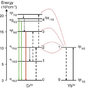
A typical system is represented by Er3+ used as emitter and Yb3+ as sensitizer. The energy level
diagram and the electron transitions giving rise to upconversion for this system are schematized in Fig 1.2.1.
Fig. 1.2.1 Energy levels of Yb3+ and Er3+ ions relevant to the energy transfer upconversion process. Initial
absorption is indicated by the black solid line narrow, the subsequent energy transfer processes by the dashed arrows, the non-radiative relaxations by dotted arrows and the final upconverted luminescence by
the green and red arrows.34
In the Er3+ ion the energy difference between the 4I
11/2 and 4I15/2 states (10350 cm-1) is similar to that
between the 4F
7/2 and 4I11/2 states (10370 cm-1). In addition, the energy difference between the 4F9/2
and 4I
13/2 states is in the same region; hence, the Er3+ ion can be excited to a higher energy level by
11
upconverted green and red emissions. Yb3+ has an extremely simple energy level scheme with only
one excited 4f level of 2F
5/2. In addition, the 2F7/2 -2F5/2 transition of Yb3+ is well resonant with the
transition energy between the 4I
11/2 and 4I15/2 states and also the 4F7/2 and 4I11/2 states of Er3+ ions,
thus facilitating the energy transfer from Yb3+ to Er3+ ions.
Usually, a higher concentration of Yb3+ sensitizer is doped in UC materials (18–20%). Yb3+ is also
12
References
1 R. Whatmore, Springer, 2007.
2 V. M. Goldschmidt, Naturwissenschaften, 1926, 14, 477.
3 H. Schmid, Multi-ferroic magnetoelectrics, Ferroelectrics, 1994, 162, 317. 4 M. Bibes and A. Barthelemy, Nature Materials, 2008, 7, 425-426.
5 J. B. Neaton, C. Ederer, U.V. Waghmare, N. A. Spaldin and K. M. Rabe, Phys. Rev. B, 2005, 71,
014113.
6 N. A. Hill and K. M. Rabe, Phys. Rev. B, 1999, 59, 8759.
7 T. Lottermoser, T. Lonkai, U. Amann, D. Hohlwein, J. Ihringer and M. Fiebig, Nature, 2004, 430,
541.
8 T. Kimura, T. Goto, H. Shintani, K. Ishizaka, T. Arima and Y. Tokura, Nature, 2003, 426, 55. 9 F. N. Sayed, B. P. Mandal, O. D. Jayakumar, A. Arya, R. M. Kadam, A. Dixit, R. Naik and A. K.
Tyagi, Inorg. Chem., 2011, 50, 11765–11772.
10 M. Eibschutz, H. J. Guggenheim, S. H. Wemple, I. Camlibel and M. DiDomenico, Phys. Lett.,
1969, 29A, 409.
11 F. N. Sayed, B. P. Mandal, O. D. Jayakumar and A. K. Tyagi, AIP Advances, 2013, 3, 072133. 12 C. Ederer and N.A. Spaldin, Phys. Rev. B, 2006, 74, 024102.
13 N. A. Hill, J. Phys. Chem. B, 2000, 104, 6694.
14 R. Seshadri and N. A. Hill, Chem. Mater., 2001, 13, 2892.
15 M. Manikandan, A. Muthukumaran and C. Venkateswaran, Journal of Magnetism and Magnetic
Materials, 2015, 393, 40–45.
16 M. Manikandan, A. Muthukumaran, C. Venkateswaran, Solid State Physics, 2014, 1, 1516-1517. 17 R.D. Shannon, Acta Crystallogr. Sect. A, 1976, 32, 751-767.
13
18 L. Mateos, M. O. Ramirez, I. Carrasco, P. Molina, J. F. Galisteo-Lopez, E. G. Villora, C. de las
Heras, K. Shimamura, C. Lopez and L. E. Bausa, Advanced Functional Materials, 2014, 24, 1509-1518.
19 N. Kodama, T. Hoshino, M. Yamaga, N. Ishizawa, K. Shimamura and T. Fukuda, Journal of
Crystal Growth, 2001, 229, 492–496.
20 A. Wu, Z. Wang, L. Su, D. Jiang, Y. Zou, J. Xu, J. Chen,Y. Ma, X. Chen and Z. Hu, Optical
Materials, 2014, 38, 238-241.
21 X. Zhang, S. Liu, X. Chen and W. Luo, Solid State Communications, 2015, 205, 33–38. 22 T. E. Littleford, R. E. Jackson and S.D. Mark, Phys. Status Solidi C, 2013, 10, 153-155.
23 M. Trevisani, K. V. Ivanovskikh, M. O. Ramirez, P. Molina, E. G. Villora, K. Shimamura, L. E.
Bausa and M. Bettinelli, Journal of Luminescence, 2014, 153, 136-139.
24 Y. Ma; J. Chen, Y. Zheng and X. Chen, Applied Optics, 2012, 51, 5432-5437.
25 J. Chen, X. Chen, A. Wu, H. Li, Y. Zheng, Y. Ma, L. Jiang and J. Xu, App. Phys. Lett., 2011, 98,
191102.
26 C-L. Pan, H-L. Liu, Y. Guo, S. Jing, H-F. Zhou and H. Wang, Wuli Xuebao, 2014, 63,
154211/1-154211/5.
27 Z-Y. Yan, B. Yan and L-P. Jia, Materials Research Bulletin, 2013, 48, 4402–4405. 28 Z-Y. Yan and B. Yan, Photochemistry and Photobiology, 2013, 89, 1262-1268. 29 F. Auzel, Acad. Sci. Paris B, 1966, 263, 819–821.
30 W.Yang, X. Li, D. Chi, H. Zhangand X. Liu, Nanotechnology, 2014, 25, 482001. 31 J. Ohwaki and Y. Wang, Jpn. J. Appl. Phys., 1994, 33, 334–337.
32 F. Auzel, D. Pecile and D. Morin, J. Electrochem. Soc., 1975, 122, 101–107. 33 F. Wang and X. Liu, Chem. Soc. Rev., 2009, 38, 976–989.
14
Chapter 2: Development of MOCVD precursors
2.1 Background studies on alkaline earth precursors
In this work, the most critical issues related to thin film fabrication are discussed from different points of view, from the precursor choice to the substrate nature. Indeed, the success of the MOCVD technique relies upon the precursor nature, the deposition parameters and the specifical used substrate. In particular, the importance of precursor nature becomes crucial for the synthesis of multicomponent systems, such as BaMF4, for which it is necessary to have suited Ba, M and F
sources. For these reasons, before growing multicomponent systems, it is of fundamental importance a preliminary study on the precursor nature and its application to the growth of single phases, e.g. barium and magnesium in the case of BaMgF4, in order to optimize all the factors that
influence the film properties.
Thermally stable and volatile Ba, Mg and F precursors are needed for the growth of these films. Group II metal precursors have always represented a great challenge in the MOCVD process since they show severe drawbacks in terms of mass transport properties due to the large size (except for Mg) and to the strong polarity of the alkaline earth metal centre.1 Wide efforts have been devoted to
the search for thermally stable and volatile alkaline-earth metal precursors and problems associated with Ba, much more pronounced due to the larger ionic radius of this metal compared to the other alkaline earth metals, have been overcome with the “second-generation” precursors formed by fluorinated β-diketonate polyether adducts.2
Concerning the precursors required for the synthesis of BaMgF4 thin films, the Ba(hfa)2tetraglyme,
and Mg(hfa)2(H2O)2diglyme adducts (Hfa=1,1,1,5,5,5-hexafluoroacetylacetone; tetraglyme=
15
metal/fluorine single sources, since previous studies have shown that these precursors act as efficient single sources for the deposition of BaF2 and MgF2 respectively.3,4,5
Hence, they were synthesized as previously reported, and applied to the growth of binary fluoride thin films, whose properties as host matrices have been investigated as well.
Due to the great interest in the SrF2 phase as host matrix for UC luminescence, the
Sr(hfa)2tetraglyme precursor has been synthesized as well3 and applied to the MOCVD growth of
SrF2 thin films.
2.1.1 Ba(hfa)
2·tetraglyme
The complex Ba(hfa)2·tetraglyme has been synthesised through a one-pot reaction between
Ba(OH)2·8H2O (2.674 g, 8.47 mmol) dispersed in a CH2Cl2 solution (35 ml), tetraglyme (1.570 g,
7.06 mmol) and Hhfa (2.94g, 14.13 mmol). The resulting mixture was refluxed under stirring for 1 h. The excess of barium hydroxide was filtered off and the product recovered from the CH2Cl2
solution, in which it is soluble. The product was purified using pentane to yield colourless crystals. The structural characterization of the present precursor has been performed by FT-IR analysis. The FT-IR spectrum of Ba(hfa)2·tetraglyme (Fig. 2.1.1.1) does not show any band in the 3500–3600
cm−1 interval thus confirming the absence of water in the coordination sphere..
Fig. 2.1.1.1 FT-IR spectrum of Ba(hfa)2·tetraglyme.
4000 3500 3000 2500 2000 1500 1000 500 0 20 40 60 80 100 T ( %) Wavelength (cm-1)
16
Peaks at 1658 cm−1 (C=O stretching vibrations) and at 1524 cm−1 (C=C stretching vibrations) are
typical of the -diketonate framework The other bands, observed in the range 1300–1100 cm−1,
represent the C–F stretchings of the hfa ligand. In addition, bands observed in the range 1100-700 cm-1 can be associated with glyme modes. Other features (at 2915, 1460 and 1377 cm−1) are typical
of the nujol used to prepare the mull.
The thermal behavior of the Ba adduct has been fully investigated by thermogravimetric analyses (TG) (Fig. 2.1.1.2). The Ba(hfa)2·tetraglyme complex is thermally stable and the derivative curve of
TG (DTG) consists of a single peak thus indicating that it evaporates quantitatively in the 180–310
◦C range, with a residue left at 350 °C of 8 %.
Fig 2.1.1.2 TG and DTG profiles of Ba(hfa)2·tetraglyme under N2 flow at atmospheric pressure in the 30–
400 ◦C temperature range.
From thermal analysis it can be concluded that the Ba(hfa)2·tetraglyme adduct shows a clean
vaporization with a low residue as requested for MOCVD applications.
50 100 150 200 250 300 350 400 Temperature (°C) 0 20 40 60 80 100 We igh t ( %) TG DTG
17
2.1.2 Mg(hfa)
2·(diglyme)
2·(H
2O)
2Herein, the synthesis and transport characteristics of the magnesium precursor of formula Mg(hfa)2
·2H2O·2diglyme [Hhfa= 1,1,1,5,5,5-hexafluoro-2,4-pentanedione, and diglyme =
(bis(2-methoxyethyl)ether)], are reported. The Mg adduct was prepared using a procedure analogous to the one described for the Ba adduct from 2.041 g (4.21 mmol) of magnesium basic carbonate source (MgCO3)4·Mg(OH)2·5H2O, 2.940 g (14.13 mmol) of Hhfa and 1.895g (14.13 mmol) of diglyme
reagents. The procedure yields reproducibly, under open bench manipulations, a clean source adduct. A slight excess of Mg carbonate favors the isolation of the product since the excess remains insoluble and can be easily filtered off. The adduct is very soluble in common organic solvents such as ethanol, chloroform, acetone, and pentane and slightly soluble in cyclohexane. It has a very low melting point and evaporates quantitatively at low temperature under vacuum and even under atmospheric pressure despite the presence of coordinated water. The FT-IR transmittance spectrum of the Mg(hfa)2·2H2O·2diglyme adduct (Fig. 2.1.2.1) shows a broad envelope with two bumps in
the 3292 and 3487 cm-1 range due to the OH asymmetric and symmetric stretching modes of
coordinated water.6 The carbonyl stretching frequency appears at 1657 cm-1, whereas peaks at 1558
and 1534 cm-1 are associated with C=O stretching and with C=C stretching vibrations,
respectively.7 The broadband observed in the 1000-1300 cm-1 range may be associated with
absorptions due to the polyether C-O bending and/or stretching overlapped with the C-F stretching. In addition, bands at 1015, 861, and 837 cm-1 can be associated with glyme modes. The C-H glyme
stretching modes, lying in the 2800-3000 cm-1 range, overlap with nujol features. In fact, the nujol
18
Fig 2.1.2.1 FT-IR spectrum of Mg(hfa)2·2H2O·2diglyme.
Thermal behavior of the Mg(hfa)2·2H2O·2diglyme adduct has been studied by thermal gravimetric
analysis (TG) experiments. Atmospheric pressure TG analysis of the Mg(hfa)2·2H2O·2diglyme
adduct shows two regions mass loss in the temperature range 40-100 °C and 110-210 °C (Fig. 2.1.2.2). The lower-temperature process, associated with a minor mass loss (∼5%) is well-tuned with the following equation
Mg(hfa)2·2H2O·2diglyme Mg(hfa)2·2diglyme + 2H2O
The remaining 95% mass is lost quantitatively in the second step, almost without residue (<1%) left. Therefore, the lower temperature process leaves an anhydrous, liquid adduct, which evaporates intact afterward. Therefore the present Mg adduct, despite the presence of water molecules in the coordination sphere, cleanly self-generates a liquid anhydrous source that represents a single source of Mg and F elements for MOCVD processes of magnesium fluoride phases.
4000 3500 3000 2500 2000 1500 1000 500 0 20 40 60 80 100 T ( %) Wavelength (cm-1)
19
Fig. 2.1.2.2 TG and TG profiles of Mg(hfa)2·2H2O·2diglyme under N2 flow at atmospheric pressure in the
30–400 ◦C temperature range.
2.1.3 Sr(hfa)
2·tetraglyme
The present strontium complex was synthesized following the same scheme of the Ba and Mg precursors. The one-pot reaction between strontium hydroxide Sr(OH)2·8H2O (2.441 g, 9.18 mmol)
dispersed in a CH2Cl2 solution (35 ml), tetraglyme (1.570 g, 7.06 mmol) and Hhfa (2.940g, 14.13
mmol) yielded the anhydrous, air-stable Sr(hfa)2·tetraglyme adduct. The FT-IR spectrum is reported
in figure 2.1.3.1. The absence of any band in the 3500–3600 cm−1 interval is indicative of a
water-free complex. The carbonyl stretching frequency appears at 1665 cm-1, while peak at 1524 cm-1 is
associated with C=C stretching. The other bands, observed at 1300–1100 cm-1, represent C-O
bending and/or stretching of the polyether ligand overlapped with the C-F stretching. In addition, the spectrum shows characteristic peaks between 750 and 1050 cm-1 which may be considered as
fingerprints of the glyme coordination to the strontium hexafluoroacetylacetonate moiety. The peaks at 2922, 1458 and 1376 cm−1 are assigned to the nujol.
. 50 100 150 200 250 300 350 400 0 20 40 60 80 100 TG We ig h t ( % ) Temperature (°C) DTG
20
Fig. 2.1.3.1 FT-IR spectrum of Sr(hfa)2·tetraglyme.
The thermal behavior of the present Sr precursor has been fully investigated by thermogravimetric analyses (TG) (Fig. 2.1.3.2). A singular sublimation step is observed. The sublimation process takes place in the temperature range 160-300 °C (residue=3% to 350 °C).
Fig 2.1.3.2 TG and DTG profiles of Sr(hfa)2·tetraglyme under N2 flow at atmospheric pressure in the 30–
400 ◦C temperature range.
The IR and TG data of the raw and sublimed adduct are in very good agreement with the characterization reported in literature.3
4000 3500 3000 2500 2000 1500 1000 500 0 20 40 60 80 100 T ( %) Wavelength (cm-1) DTG TG 50 100 150 200 250 300 350 400 0 20 40 60 80 100 Temperature (°C) We igh t ( %)
21
2.2 Applications of Ni precursors to NiO films growth
In this thesis, a Metal Organic Chemical Vapor Deposition approach is used to the fabrication of BaNiF4 phases (par. 3.1). To this aim, fluorinated -diketonate Ni(II) complexes may be envisaged
as Ni-F single sources for the fabrication of Ni-F based phases as thin films.
In addition, a reproducible MOCVD process requires thermally stable and volatile enough single sources to provide molecular integrity during the mass transport. Low-melting architectures are also desired to allow constant evaporation from the liquid phase for long time intervals.
To date, -diketonate complexes with 2,2,6,6-tetramethyl-3,5-heptanedione (Hthmd) and acetylacetone (Hacac) ligands have been widely used as MOCVD sources for NiO films.8 These
precursors suffer, however, from some drawbacks associated with their high melting points [228°C for Ni(tmhd)29 and 240 °C for Ni(acac)210] and with the presence of H2O molecules in the
coordination sphere. In addition, they do not have F atoms in their structures, thus they can not be applied as fluorine sources to the synthesis of nickel fluoride phases.
Therefore, two fluorinated precursors have been tested: the Ni(hfa)2tmeda and the Ni(tta)2tmeda11
[(H-hfa =1,1,1,5,5,5-hexafluoro-2,4-pentandione, Htta = 2-thenoyltrifluoroacetone, tmeda = N,N,N',N'-tetramethylethylendiamine)]. In particular, the synthesis and characterization of the transport properties of both precursors are reported in the following.
A comprehensive systematic study for the MOCVD deposition of NiO films relating the use of the two precursors on the structural, morphological and functional properties of the deposited layers has been assessed. The correlation between the nature of the nickel β-diketonate precursor and the properties of the NiO film has been addressed.
The Nickel oxide (NiO) is among the most widely investigated transition metal oxides (TMOs), and its properties and applications deserve a more detailed description. Nickel oxide actually represents a model compound for TMOs with the sodium chloride structure.12 It exhibits only a very small
22
deviation from the ideal stoichiometry, at difference with the cobalt oxide (CoO) and especially the wüstite iron oxide (FeO) phase.
NiO has also drawn much attention due to its utilization for several applications, such as gas sensors,13,14 catalysts,15,16 and electrochromic devices.17-20 Other applications regard its use as
transparent conducting oxide (TCO) films. TCO films such as indium oxide, tin oxide and zinc oxide, are of practical use as transparent electrodes and window coatings, but they are all n-type semiconductors. A desirable hole injecting contact would be based on the injection into the valence band of a p-type semiconducting oxide. NiO films is one of the potential candidates for p-type TCO. Nickel oxide is known to become a p-type semiconductor when its composition deviates from stoichiometry or when monovalent atoms, such as Li+,21,22 are added, while pure stoichiometric NiO
is an insulator with high resistivity (ρ > 1013 Ω.cm) at room temperature. Due to their electric
properties, p-type semiconducting nickel oxide films have been used as efficient-enhancing anode interfacial layers in polymer bulk-heterojunction,23-25 and dye-sensitized solar cell21,26-29 and as hole
transporting30 or as electron blocking31 layer in light-emitting devices.
Thin films of NiO, due to their antiferromagnetic properties with a Néel point (TN) of 523 K, are
also very useful as the antiferromagnetic layer of spin-valve superlattice films. Pure nickel oxide exhibits antiferromagnetic ordering, with planes of opposite spins being repeated in alternating order along the [111] direction. Below the Néel temperature, the magnetic ordering in NiO is accompanied by a slight rhombohedral distortion (at 20°C, a =2.9518 Å, α=60.42°).32 Magnon
excitations in pure NiO nanoparticles and single crystals have been successfully studied by Raman spectroscopy:33-35 the strong magnetic Raman response is caused by the Ni-O superexchange
23
2.2.1 Impact of precursors and substrate on NiO film properties
Two different nickel sources have been synthesized and applied: Ni(tta)2•tmeda and Ni(hfa)2•tmeda.
The synthesis and characterization of Ni(tta)2•tmeda have been reported elsewhere.11 Herein, it is
presented a new strategy for the synthesis of Ni(hfa)2•tmeda, whose synthesis had been previously
reported.36 The volatile and thermally stable Ni(hfa)
2•tmeda complex was prepared by the reaction
of Ni(CH3COO)2●4H2O (1.932 g, 7.763 mmol) suspended in dicloromethane (50 ml) with tmeda
(0.821 g, 7.065 mmol) and H-hfa (2.940 g, 14.130 mmol). The mixture was refluxed, under stirring, for 1 h. The solution was collected by filtration under vacuum and the excess of Ni(CH3COO)2•4H2O was filtered off. Green-emerald crystals were obtained upon evaporation of
the solvent and were washed two times in pentane. Upon filtration, green emerald crystals were recovered. The reaction yield was 88 %. The melting point of the crude product was 103-107 °C/760 Torr. The thermal behavior of the present Ni(tta)2•tmeda and Ni(hfa)2•tmeda precursors has
been investigated by thermogravimetric (TG) analyses at atmospheric pressure in a purified nitrogen flow (Fig. 2.2.1.1). The thermogravimetric first derivative (DTG) of Ni(tta)2•tmeda
consists of a single peak, thus indicating that the precursor evaporates quantitatively in the 200-330°C range, with a residue left at 350°C lower than 2%. Same behaviour can be observed for Ni(hfa)2•tmeda whose evaporation occurs in the temperature range 120-200 °C, with a residue left
of about 2% at 350 °C. It can be concluded that both Ni(tta)2•tmeda and Ni(hfa)2•tmeda precursors
24
Fig. 2.2.1.1 TG and DTG profiles of Ni(hfa)2•tmeda and Ni(tta)2•tmeda complexes under N2 flow at
atmospheric pressure in the temperature range 30-400°C.
In figure 2.2.1.2, the differential scanning calorimetry (DSC) curves of the Ni(tta)2•tmeda and
Ni(hfa)2•tmeda are reported. The DSC scans show evidence of the endothermic peaks due to
melting at 151.3 °C and 106.7 °C respectively for Ni(tta)2•tmeda and Ni(hfa)2•tmeda. Both
precursors evaporate from melts in the temperature ranges 300-330 °C and 125-195 °C, respectively.
25
NiO films were prepared in a reduced-pressure, horizontal, hot-wall MOCVD reactor from the Ni(tta)2•tmeda and Ni(hfa)2•tmeda sources contained in a resistively heated alumina boat.
Quartz and LaAlO3 (001) substrates were used for the depositions. In this study, the precursor
evaporation temperature was kept at 170 °C for Ni(tta)2•tmeda and 90°C for Ni(hfa)2•tmeda,
whereas the reactor temperature was kept in the 350-550 °C range. Ar (150 standard cubic centimetres per min, sccm) and O2 (50, 200 or 600 sccm) flows were used as carrier and reaction
gases, respectively. Depositions were carried out for 60 min, yielding films of thickness in the range 170-250 nm depending on the deposition temperature and precursor nature. The total pressure in the reactor was about 2-6 Torr.
Quartz and LaAlO3 (001) single crystal substrates have been chosen in view of specific
applications. In particular, quartz has been used to test the optical properties, while the LaAlO3
substrate is interesting to test the antiferromagnetic properties, since a very important issue in the fabrication of magnetic thin films is to find a substrate with a good lattice match vs. the growing film. The structure of films, as determined by XRD, is summarised for deposition on quartz substrates in figure 2.2.1.3.
Specifically, figures 2.2.1.3a and 2.2.1.3b show the XRD patterns of NiO films deposited on quartz substrates in the temperature range 350-550°C with an oxygen flow of 200 sccm from the Ni(tta)2•tmeda and Ni(hfa)2•tmeda precursors, respectively. For both the precursors, 350°C yields
amorphous NiO films, while at higher temperatures of 450°C and 550°C, the films are polycrystalline, as inferred by the 2θ peaks at 37.30, 43.35 and 62.90° corresponding to the 111, 200 and 220 reflections, respectively. Note that only the reflection with hkl all odd or all even are observed due to the face-centered cubic lattice. In addition, the observed intensities do not always match those found for the polycrystalline powder as reported in the ICDD N. 47-1049. In particular, the I(200)/I(111) ratio (Figure 2.2.1.3c) and the full width at half maximum, FWHM, of the 200 peak, (Figure 2.2.1.3d) as a function of temperature and precursor type, indicate that the
26
Ni(tta)2tmeda at 550°C results in NiO films with a slight preferential orientation along the <001>
direction.
Fig. 2.2.1.3 X-Ray diffraction patterns of NiO films grown on quartz substrate at various temperature
using the precursors (a) Ni(tta)2•tmeda and (b) Ni(hfa)2tmeda. (c) The evolution of the I(200)/I111) ratio
and FWHM (200) as a function of temperature and precursor type is also shown.
Therefore, considering that XRD data indicate 550°C as the temperature condition to produce NiO films of better crystallinity, the unit cell parameter a has been extrapolated for films grown under these conditions from the two precursors following the diagram reported in figure 2.2.1.4. The extrapolated a-axis value of films grown from the precursor Ni(tta)2•tmeda is 4.1750 Å. On the
other hand, the a-axis parameter of films grown from the Ni(hfa)2•tmeda is 4.1883 Å. The axis of
the films grown from the Ni(tta)2•tmeda, that compares well with the theoretical one of 4.17710 Å
for the bulk NiO phase, indicates that these films are of good quality and stoichiometric compared to the bulk system.
27
Fig. 2.2.1.4 Diagram for extrapolation of a-axis parameter of NiO phase. Red points refer to the NiO film
obtained from Ni(hfa)2•tmeda precursor, black points refer to the NiO film obtained from Ni(tta)2•tmeda.
Therefore, NiO films have been grown on LAO (001) substrate under the optimized conditions obtained for depositions on quartz from the Ni(tta)2•tmeda. The LAO substrate has been chosen to
have a good lattice match, because if the lattices are well suited for one another the surface of a thin film appears smooth and flawless. If the spacing between atoms in the substrate is too different from that of the overlying film, however, then the film may exhibit wrinkling, clumping, or other defects and these surface characteristics may affect the magnetic properties. The LAO substrate has a perovskite structure, whose unit cell can be described as pseudo-cubic with a lattice constant aps = 3.792 Å, thus a mismatch of 10.6 % occurs for the NiO/LAO system. Figure 2.2.1.5 presents the XRD diffraction pattern of the sample deposited on LAO (001) at 550 °C and exhibits only the NiO 002 and 004 reflections at 2=43.30° and 95.35° in addition to the peaks at 2 = 23.45°, 2 = 48.15° and 2 = 75.30° associated with the LAO 001, 002 and 003 reflections, respectively. Therefore, the NiO films grown on LAO (001) are purely <001> oriented. The grains dispersion has been investigated by measuring the rocking curve of the 002 reflection at 43.30° (Figure 2.2.1.5b). The full width at half maximum (FWHM) value of 0.94° indicates a good out-of-plane alignment of NiO films. The in-plane-alignment has been studied by recording the (111) pole figure (2 = 37.25°) of NiO films (inset in Figure 2.2.15a). The pole figure shows four poles observed at =
28
54° every 90° degrees of , as expected for a cubic symmetry. In addition, the in-plane relationship of NiO films relative to the underlying LAO substrate has been obtained from -scans of the NiO/LAO system (Figure 2.2.1.5c). -scans have been recorded using as poles the NiO 111 reflection (2 = 37.25°) and the LAO 111 reflection (2 = 41.20°) at tilt angles of 54°. The four peaks from the NiO (111) planes are coincident with the (111) LAO positions. This clearly demonstrates that a cube-on-cube growth is observed for the NiO on LAO substrate, thus the [100] and [010] axis directions are aligned for the film and the substrate (i.e. NiO <100>║LAO <100>).
Fig. 2.2.1.5 a) XRD pattern of a film deposited on LAO (001) substrate at 550°C using the Ni(tta)2tmeda
precursor; the inset reports the 111 pole figure (2=37.25°) of the NiO film; b) rocking curve of 002
reflection of the epitaxial NiO film; c) -scans using the 111 reflections as poles for the NiO and LaAlO3
29
These findings may be compared with the studies on heteroepitaxial growth of NiO on AlGaN.37-39
In this case, due to the hexagonal structure of the substrate, an epitaxial growth of the {111} NiO planes on the (0001) substrate plane occurred. The study of the structural properties of the NiO films is corroborated by Raman measurements. Raman spectroscopy has been used as a non-nondestructive investigation of the structure and stoichiometry of NiO films, since NiO electronic structure, captured in its Raman spectrum, clearly evolves with its stoichiometry, quality and antiferromagnetic properties. The vibrational bands corresponding to the one-phonon (1P) longitudinal optical (LO) (at 570 cm-1) modes, the two-phonon (2P) mode 2TO (870 cm-1) and
2LO (at 1100 cm-1) modes, and the band due to a two-magnon (2M) scattering at 1490 cm-1 are
observed (Figure 2.2.1.6). The 1P broad band is a disorder-induced band that originates by Ni vacancies and its intensity has been related40 to the film quality, i.e., the lower the intensity, the
better the film quality, because of a lower density of Ni-vacancies and, consequently, a better stoichiometry. The intensity of the 1P band measured for films of comparable thickness under the same Raman acquisition conditions (measured also the same day) plotted in figure 2.2.1.6e shows that the film quality (in terms of Ni-vacancies) is significantly better for the Ni(tta)2tmeda
precursor. Another important difference between films grown from the two precursors comes out by analyzing the region around 1490 cm-1 of the characteristic two-magnon (2M) scattering band; its
presence for the films from Ni(tta)2tmeda indicates that films are in the antiferromagnetic phase.
Conversely, bands at 1350 cm-1 and 1600 cm-1 (Figure 2.2.1.6a, b) indicates carbon contamination
30
Fig. 2.2.1.6. Raman Spectra of NiO films on quartz from Ni(hfa)2 tmeda at (a) 450°C and (b) 550°C and
from Ni(tta)2 tmeda at (c) 450°C and (d) 550°C. (e) Evolution of the 1P intensity as a function of
temperature and precursor.
The NiO films have mirror-like surfaces and are homogeneous also in terms of morphology, over the whole area, as indicated by FE-SEM and AFM images, shown in figure 2.2.1.7. For both precursors, the grain size increases with the increase of deposition temperature. At the lowest temperature of 350°C, the surfaces of films deposited from both precursors are very smooth and very small grains of about 50 nm are found (Figure 2.2.1.7a and b). This is in accordance with the amorphous nature of the films. At higher temperature, films grown from the Ni(tta)2tmeda show
homogeneous surfaces with cubic grain dimensions going from about 90 nm at 450°C (Figure 2.2.1.7c) to 130 nm at 550 °C (Figure 2.2.1.7e). In the case of films deposited from the Ni(hfa)2tmeda, a flat, homogeneous surface with small grains of 100 nm is observed at 450°C
31
(Figure 2.2.1.7d), while large structured leaf-like grains of 250-300 nm are found at 550°C (Figure 2.2.1.7f). The increases of the grain size with temperature is expected, since higher temperatures give rise to higher mobility of the atoms/molecules on the surface, thus favoring growth vs. nucleation and producing films with larger grains. The morphology of films deposited at 550 °C on LAO (001) substrate (Figure 2.2.1.7g) exhibits a smooth surface with crystalline cubic grains of about 70-80 nm.
Fig. 2.2.1.7 FE-SEM images of NiO films deposited on (a-f) quartz substrate and (g) on LAO from (a, c, e,
g) Ni(tta)2•tmeda and (b, d, f) Ni(hfa)2•tmeda. The corresponding 1µmx1µm AFM topographical images
(c’, d’, e’, f’ and g’) are also shown.
Dependence of grain size on temperature is reported in figure 2.2.1.8a. AFM images, reported as appended figures, confirm the FE-SEM morphology giving quantitative information on the root mean square (RMS) roughness. Indeed, results, summarized in figure 2.2.1.8b, show a smoother morphology for films from Ni(tta)2tmeda on both quartz and LAO substrates with a RMS
32
roughness going from 3 to 5 nm, while an increase of roughness with temperature from 2.5 nm to 45 nm is observed for films from Ni(hfa)2tmeda.
Fig. 2.2.1.8 Evolution of the (a) grain size and (b) roughness (RMS) as a function of temperature, precursor and substrate.
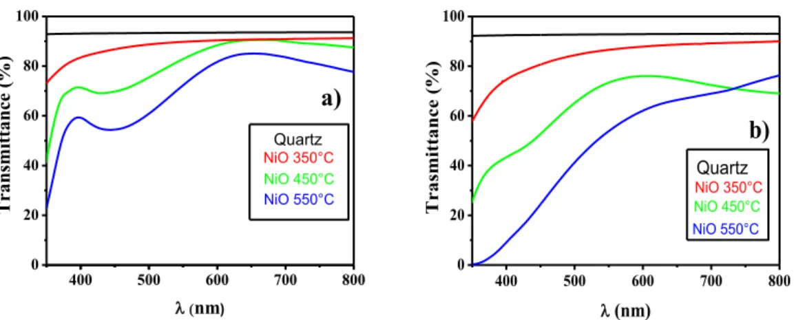
The optical properties have been tested through UV-Vis and ellipsometric measurements. The transmittance spectra show that the NiO films from Ni(tta)2tmeda (Figure 2.2.1.9a) are highly
transparent in the visible region with optical transmission nearly 90% between 450 nm and 800 nm for the amorphous layer grown at 350°C. On increasing the deposition temperature the optical transmission is approximately 80% between 550 and 800 nm. The optical transmittances of films grown from the Ni(hfa)2•tmeda, reported in figure 2.2.1.9b, result to be worse than those observed
for films obtained from Ni(tta)2•tmeda.
Therefore, the UV-Vis spectral data point to better transparent properties for the NiO films grown at 450°C from the Ni(tta)2tmeda.
33
Fig. 2.2.1.9 Transmittance spectra of NiO films on quartz from (a) Ni(tta)2•tmeda and (b) Ni(hfa)2•tmeda
as a function of temperature.
Figure 2.2.1.10a shows the spectra of the refractive and extinction coefficient derived by the ellipsometric analysis for the NiO film grown at 450°C from the Ni(tta)2•tmeda. The comparison of
the spectra of the absorption coefficient also shows a good agreement with the NiO single crystal. The observed slight difference is due to a lower density of the films due to their polycrystalline structure.41
Fig. 2.2.1.10 (a) Spectra of the refractive index and absorption coefficient, derived by the ellipsometric analysis, of the NiO film on quartz.; (b) Evolution of the % voids (measure of the film density) as a function of temperature and precursor.
400 500 600 700 800 0 20 40 60 80 100 Tr ansmittance (%) nm) NiO 450°C NiO 550°C NiO 350°C a) Quartz 400 500 600 700 800 0 20 40 60 80 100 Quartz Tr asmi tt ance (%) (nm) NiO 450°C NiO 550°C NiO 350°C b)
34
The densest film is deposited at 450°C from Ni(tta)2tmeda; the increasing of voids fraction in
figure 2.2.1.10b indicates that the density of the NiO films decreases with the Ni(hfa)2tmeda
precursor and with the increase of the temperature, consistently with the change in morphology seen in Figure 2.2.1.7 (larger grains and less compact microstructure observed with the increase in temperature). From the (E)2 vs. energy, E, plot, a direct optical gap of 3.7 eV has been estimated
that compares well with the value of 3.8-4.0 eV of the single crystal NiO.42 As for the role of the O 2
flow, previous studies indicated43 that the quality of NiO also depends on the O
2 quantity.
Therefore, using the Ni(tta)2tmeda precursor, NiO films have been deposited at 450°C under three
different O2 flows of 50, 200 and 600 sccm. Figure 2.2.1.11 shows the optical properties, in the
region of the absorption edge, of the NiO films derived by the ellipsometric analysis as a function of O2 flow on quartz substrate.
Figure 2.2.1.11 Absorption coefficient around the fundamental absorption edge of NiO films grown on
quartz at different O2 fluxes of 50, 200 and 600 sccm. The inset shows the corresponding value of the
refractive index, n, at the photon energy of 2 eV.
The higher refractive index and density and the sharper absorption edge indicate that the optimal O2
flow is 200 sccm. Specifically, for excess of O2 flow (e.g. 600 sccm), nickel vacancies alter the
band structure44 and result in a low energy (2-3 eV) absorption peak correlated to nickel 3d8-3d8*
transitions. Conversely, at lower O2 flow (e.g 50 sccm) O2- vacancies inhibit the previous peak, but
35
To summarize, the present results indicate that NiO films obtained from Ni(tta)2tmeda precursor
show both morphological and optical properties better than those found for samples grown from Ni(hfa)2tmeda, thus indicating that the former precursor is more suitable to the MOCVD growth of
high quality NiO films. Note that the transparency of the layer and the very low interface and surface roughness make these films potentially interesting for applications in light-emitting devices30 or photovoltaics.45,46
2.2.2 MOCVD fabrication of NiO dielectrics
Depending on the targeted application, the NiO thin films are grown on different substrates and with a specific stoichiometry, in order to obtain the desired electrical characteristics. In particular, the stoichiometric NiO can be considered an intrinsic semiconductor (thus a semi-insulating material), which by heating treatments at high temperatures can combine with atmospheric oxygen becoming a fairly good electrical conductor (NiOx).47,48 This behavior has been also shown by other
transition metal compounds containing the metal in two oxidation states.49,50 In the case of NiO x
(x>1), the Ni cations possess +2 and +3 oxidation states and the excess of oxygen anions creates vacant sites normally occupied by nickel ions. In order to maintain the electrical neutrality inside the crystal, Ni2+ slightly oxidizes to Ni3+, thus electrons can be transferred from Ni2+ ions to the
adjacent Ni3+ ions through a mechanism of “electronic jumping” which leaves behind a gap.51,52
Therefore, NiO can be used either as insulator or as p-type semiconductor, both characteristics make it an appealing material for microelectronics applications. A growing field inmicroelectronics is the development ofwide band gap semiconductor devices and in particular those based on AlGaN/GaN heterostructures.53-55 In this context, one of the main issues to be addressed is the
growth of a suitable dielectric to optimize the critical device parameters, such as channel mobility, parasitic capacitance and gate leakage current. Some oxides, for instance SiO2, Al2O3, Ga2O3, HfO2,
36
Here, NiO thin films are proposed because of their potentially low lattice mismatch if epitaxially grown on AlGaN/GaN heterostructures and because of their high permittivity value (11.9).61
Metal Organic Chemical Vapor Deposition (MOCVD) approach is used, since among the different fabrication methods, it represents a reliable and reproducible technique for large-scale production of highly uniform films in both thickness and composition. Moreover, it is noteworthy that it is the dominant technique for the commercial production of GaN-based materials. Hence, the possibility to grow also the gate dielectric by MOCVD could be a driving force to establish this technology in nitride-based devices.38,39
Several depositions have been conducted to verify the possible use of NiO thin films in GaN-based transistors. The experimental parameters have been appropriately varied in order to optimize the film growth conditions and to investigate their effects on the electrical properties. Firstly, the deposition temperature has been varied during the growth. In particular, depositions of NiO thin films have been carried out at both low (500 °C) and high (750 °C) temperatures and with a constant oxygen flow (200 sccm), in order to study the influence of deposition temperature on the structural properties of the obtained films. Fig. 2.2.2.1a shows the XRD patterns of NiO films deposited under the two temperatures. In both cases, the obtained NiO showed a preferential <111> growth direction since, apart from the peaks due to the AlGaN/GaN system in the 30–36.5° and 69– 79° 2θ ranges, the other two peaks at 37.4° and 79.8° can be related to the 111 and 222 reflections of the NiO phase (ICDD card # 47-1049). In order to complete the XRD investigation, the grain dispersion along the c-axis has been evaluated by recording the rocking curves around the 111 NiO reflection. The fullwidth at halfmaximum (FWHM) of the peaks is similar for both films deposited at different temperatures, i.e., 0.35° (500 °C) and 0.3° (750 °C), thus indicating an excellent out-of-the plane alignment of out-of-the NiO films (Fig. 2.2.2.1b). Thus, it can be concluded that out-of-the deposition temperature does not significantly affect the structural properties of the deposited films, which in any case are [111] oriented. In addition to the studies on the structural properties, morphological characterization has been performed using FE-SEM and TEM investigations.
37
Fig. 2.2.2.1 XRD patterns (a) of NiO films deposited at 500 °C and 750 °C. Rocking curves (b) using the
(111) NiO reflection.
Fig. 2.2.2.2 shows the FE-SEM images of the surface morphology of samples deposited at low and high temperatures and using oxygen flows of 200 and 500 sccm. These two oxygen flow values have been used as representatives for the samples deposited in the 50–200 sccm and 300–500 sccm ranges, respectively. In low temperature deposited samples (Fig. 2.2.2.2a and b) the formation of small grains has been observed. The sample deposited using a 200 sccm O2 flow does not show
defined grains, which in turn are quite visible in the sample obtained with a 500 sccm O2 flow.
However, in both films the presence of surface cracking has been observed. The FE-SEM images of samples deposited at 750 °C with oxygen flows of 200 and 500 sccm are shown in Fig. 2.2.2.2c and d. In both cases, larger grains are formed with respect to the case of depositions carried out at 500 °C and also in this case a higher O2 flow provided more defined grains. In order to improve the
morphological characteristics and to avoid the surface cracking, further depositions have been carried out on 45° tilted substrate and setting a very slow (1 °C/min) cooling rate down to room
38
temperature after the deposition. In fact, the observed cracks could be due to the different thermal expansion coefficients for the NiO film (14.5 × 10⁻⁶ K−1) and the substrate (3.17 × 10⁻⁶ K−1).
Fig. 2.2.2.2 FE-SEM micrographs of NiO films deposited: (a) at 500 °C with 200 sccm oxygen flow, (b) at 500 °C with 500 sccm oxygen flow; (c) at 750 °C with 200 sccm oxygen flow, (d) at 750 °C with 500 sccm oxygen flow, (e) at 500 °C with 200 sccm oxygen flowand tilted substrate, (f) at 750 °C with 200 sccm oxygen flow and tilted substrate.
In Fig. 2.2.2.2e and f samples deposited at 500 °C and 750 °C, with substrate tilting and using a 200 sccm oxygen flow are shown. All the films obtained under these conditions show a compact grain distribution and the absence of surface cracking. Moreover, for applications in microelectronics two important parameters have to be considered in order to get the improved performances: the dielectric thickness should not exceed a few tens of nanometers and the quality of the dielectric/substrate interface should be free from intermediate layers and/or defects. In this context, films obtained without surface cracking have been investigated through cross-section TEM analysis
39
to evaluate the thickness and the interface quality. Fig. 2.2.2.3 shows the cross-sectional TEM images of both films deposited at low (500 °C) and high (750 °C) deposition temperatures. The sample obtained at low temperature (Fig. 2.2.2.3a) shows very compact grains, forming a continuous layer with a thickness of about 15 nm. The sample obtained at high temperature (Fig. 2.2.2.3b) shows a completely different morphological profile, as previously evidenced by FE-SEM surface images. In fact, in this case the film thickness is about 30 nm, and the grains have pyramidal shape, thus resulting in a remarkable surface roughness. The film/substrate interface quality has been studied by high resolution TEM images. As can be seen in Fig. 2.2.2.3c, no intermediate layers are visible at the interface, thus ruling out any interaction and/or oxidation of the substrate. Moreover, the Fast Fourier Transform (FFT) image (Fig. 2.2.2.3d), collected at the interface, clearly points out the epitaxial growth of the NiO films. In fact, the external spots related to the NiO are perfectly aligned to the internal ones from the AlGaN, indicating that the NiO lattice is not rotated with respect to the underlying substrate lattice. In particular, the spots related to the [111] NiO direction are aligned and almost overlapped to the spots from [001] AlGaN/GaN direction, and the NiO [110] and [311] directions are parallel to the [110] and [112] directions of the AlGaN/GaN substrate. Moreover, to complete the structural investigation, in-plane TEM image and electron diffraction data have been recorded on NiO films grown at 500 °C. The in-plane TEM image (Fig. 2.2.2.3e) shows small grains of about 20 nm wide. The related electron diffraction pattern (Fig. 2.2.2.3f) consisted of spots forming two hexagonal patterns (white circles) at 2.77 Å and 1.59 Å plane distances which can be related to (100) and to the (110) AlGaN/GaN planes, while spots forming the hexagonal pattern (red circles) at 1.47 Å can be related to the (220) NiO planes. The NiO spots are perfectly aligned to the AlGaN/GaN spots at 1.59 Å. Hence, it is possible to conclude that an epitaxial growth of the {111} NiO planes on the (0001) substrate plane occurred and the following relationships are present:
[111]NiO ‖ [0001] AlGaN/GaN [110]NiO ‖ [11−20] AlGaN/GaN.