Francesco Rizzo
Efficient delta-sigma ADC for mobile
audio applications based on a LabVIEW
assisted architectural design flow
Anno 2012
UNIVERSITÀ DI PISA
Scuola di Dottorato in Ingegneria “Leonardo da Vinci”
Corso di Dottorato di Ricerca in
DENOMINAZIONE
Ad Alessia
Che, da quando incrociato la mia strada non ha mai smesso,
di ispirare i miei pensieri e dare un senso ad ogni passo del mio cammino. Sasa
I
SOMMARIO
Questo lavoro di tesi è il risultato della fruttuosa collaborazione tra l’azienda multinazionale ST-Ericsson e il Dipartimento di Ingegneria dell’Informazione dell’Università di Pisa. ST-Ericsson è una delle aziende ”leader” nei mercati dei “modem“ e dei processori in banda base. Il gruppo di “mixed signal design“ nell’area di Zurigo (Svizzera) unitamente al gruppo basato a Bangalore (India) hanno, tra gli altri obbiettivi, la continua ricerca di soluzioni per migliorare l’efficienza ed il costo dei sotto-sistemi audio. Questa è stata quindi la base di lavoro per l’inizio di una collaborazione con l’accademia su tali temi.
Lo studio è iniziato con una valutazione dello stato dell’arte dei “computer aided design tool” (CAD tool) per gli studi architetturali e per la validazione dei progetti dei convertitori delta-sigma sia in banda audio sia per applicazioni a larga ampiezza di banda, riscontrando una mancanza di flessibilità nell’area dei flussi per la scelta di architetture orientate al progetto. Sulla base di tali evidenze è stato sviluppato un nuovo “software” implementato in LabVIEW e finalizzato a guidare la scelta dei parametri di progetto di un convertitore analogico-digitale (ADC) delta-sigma. Tale “CAD tool” considera la minimizzazione dell’area di silicio già nella scelta dell’architettura lasciando al progettista la possibilità di implementare dei requisiti addizionali per la minimizzazione dell’area piuttosto che scegliere i parametri di progetto (coefficienti della risposta in frequenza) con il solo fine di ottenere le prestazioni desiderate.
L’architettura della catena di “uplink” del processore in banda base è stata inoltre riprogettata e la funzionalità di alcuni blocchi è stata implementata nel ADC. Il controllo del guadagno, tradizionalmente effettuato da un amplificatore a guadagno variabile o “programmable gain amplifier” (PGA) attivato in corrispondenza degli attraversamenti dello zero rilevati da un “zero crossing detector” (ZCD), è stato inserito nell’anello di reazione del ADC attraverso un banco di condensatori selezionabili tramite controllo digitale. Gli effetti della commutazione del guadagno sul “dithering” e sulla traslazione del “idle-tone” sono state esaminati e sono state proposte delle soluzioni. Questo ha aperto alla possibilità di migliorare la qualità delle transizioni di guadagno attraverso un controllo a modulazione di larghezza dell’impulso o “Pulse Width Modulation” (PWM) che consente una variazione del guadagno e di conseguenza del segnale audio, molto più graduale rispetto a quanto avviene nelle soluzioni attualmente disponibili sul mercato.
Infine un ADC in banda audio con area pari a 0.073 mm2 e consumo di corrente pari a 950 µA da una tensione di alimentazione di 2.3 V, è stato realizzato in tecnologia CMOS 40nm. Il progetto è stato validato tramite la caratterizzazione sperimentale sia su un microchip di silicio a se’ stante contenente il solo ADC, sia sulla catena audio del processore in banda base G4860 che sta per essere adottato da Samsung per una prossima generazione di telefoni cellulari.
Tra i principali obiettivi innovativi raggiunti si hanno:
(i) Riduzione del 15% dell’area occupata dai condensatori commutati rispetto alle soluzioni di ADC riportati in letteratura con simili prestazioni, (ii) riduzione del 25% in area e del 30% in corrente nella catena di “uplink” audio sviluppata per un progetto GSM commerciale per mezzo dell’eliminazione sia del PGA che dello ZCD nel “front-end” audio, (iii) maggiore gradualità nel cambiamento del guadagno rispetto i dispositivi esistenti grazie ad una tecnica di controllo originale che è stata proposta per l’ottenimento di un brevetto da parte di ST-Ericsson.
ABSTRACT
This work is the result of a fruitful collaboration started in 2009, between ST-Ericsson and the Department of Information Engineering of the University of Pisa (namely, Dipartimento di Ingegneria dell’Informazione, Universita’ di Pisa). ST-Ericsson is a multi-national enterprise leader of the mobile telephony modem and baseband processors markets. The mixed signal design group based in the Zürich (Switzerland) together with the group based in Bangalore (India) among other targets has been looking at solutions for improving the efficiency ad costs of the audio subsystem. This has been the baseline to establish the collaboration in the topic with the academia.
The activity has started with an evaluation of the state-of-the-art tools for architectural studies and design validation of delta-sigma converters both for audio and large bandwidth applications. The evaluations of the state of the art have shown a lack of flexibility in the area of the design flow oriented to architectural choice. Based on this evidence, a new software has been implemented in LabVIEW in order to assist the choice of the design parameters of delta-sigma analog to digital converter (ADC). This tool considers also the minimization of silicon area in the choice of the architecture, letting to the designer the possibility to carry out additional area minimization constraints rather than only using the performance criteria for defining the coefficients of the frequency response.
Additionally, the architecture of the audio “uplink” path of the baseband subsystem has been reconsidered and the functionality of some building block has been embedded in the ADC. The gain control, traditionally performed by a programmable gain amplifier (PGA) activated in correspondence with the zero crossing detected by means of a zero-crossing detector (ZCD), has been inserted in the feedback loop of the delta sigma structure allowing the gain selection by means of a digitally controlled selection of capacitors. The implication of the gain switching in the ADC on the dithering and offset insertion has been analyzed and solutions have been proposed.
This has opened the possibility to improve the quality of the gain transition by mean of a Pulse Width Modulation (PWM) control of the gain change with the aim of obtaining a much smoother audio signal amplitude change compared to the state-of-the-art solutions available on the market.
Finally, an audio ADC featuring 0.073 mm2 silicon area, 950 µA current consumption from a 2.3 V power supply, has been fabricated in 40nm CMOS technology. The results obtained during the design phase have been validated by means of experimental characterization on test-chips, both on a standalone ADC microchips and the entire audio path of the G4860 baseband which is going to be adopted by Samsung for the next-generation cellular phones, proofing the concepts proposed and developed during this doctoral studies. The main achievements can be summarized as follows:
(i) 15% reduction of the switching capacitor area compared to existent audio ADC featuring similar performance, (ii) 25% reduction of in current and 30% of area in the uplink path developed for commercial GSM projects by eliminating the PGA and ZCD of the audio front-end, (iii) smoother gain transition with respect to the state-of-the-art devices by means of an original control technique which has been submitted for patent granting by ST-Ericsson.
III
INDEX
SOMMARIO ... I
ABSTRACT ... II
INDEX ... III
INTRODUCTION ... 1
1. A FLOW TO SUPPORT THE CHOICE OF AN ARCHITECTURE FOR A
DELTA-SIGMA ADC ... 2
1.1 Introduction ... 2
1.2 LabVIEW
TMbased design and benchmarking tool ... 2
1.3.1 Software concept ... 2
1.3 Shaping of Transfer function ... 5
1.3.1 Noise shaping ... 5
1.3.2 Open and Closed Loop Frequency responses ... 7
1.4 Stability checks ... 8
1.5 Setup and simulation panel ... 8
1.6 Application examples ... 10
1.6.1 Audio ADC ... 10
1.6.2 Large bandwidth ADC ... 12
2. ARCHITECTURES MAPPING INTO DESIGN ... 14
2.1 Introduction ... 14
2.2 Architecture mapping ... 14
2.2.1 Audio bandwidth ADC example ... 14
2.2.2 Large bandwidth ADC case ... 18
3. PWM GAIN CONTROL TECHNIQUE IN A DELTA-SIGMA AUDIO ADC
FOR MOBILE APPLICATION ... 20
3.1 Introduction ... 20
3.2 Mobile telephone uplink path ... 20
3.3 Uplink path: from microphone interface to the ADC input 20
3.3 Gain control in the audio uplink path for mobile
applications ... 21
3.3.1
The glitch-free gain switching method ... 21
3.3.2
Parameters tuning for gain switching ... 25
4. DITHERING AND OFFSET INSERTION IN A VARIABLE GAIN LOOP28
4.1 Introduction ... 28
4.2
Dithering in a variable gain delta sigma loop ... 29
4.3
Idle tone shifting by offset insertion ... 30
4.4
Conclusions ... 32
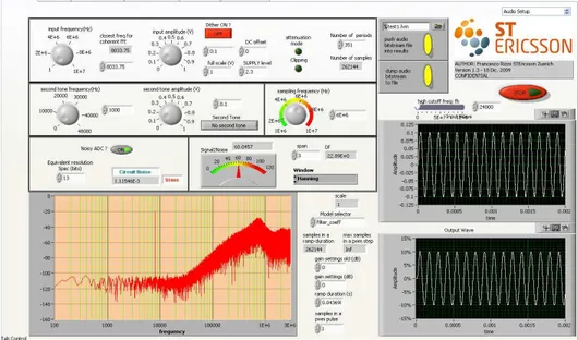
5. VALIDATION ENVIRONMENT AND SILICON RESULTS... 33
5.1 Test Concept ... 33
5.2 Uplink path in the G4860 system test results ... 34
5.2.1 Max input voltage (at Total Harmonic Distortions
≤
1%) ... 37
5.2.2 Noise spectrum,Voltage Noise, max SNR ... 38
5.2.3 Uplink gain ... 39
5.2.4 THD vs Vmic0 ... 40
5.2.5 SINAD (100Hz-24kHz) ... 42
5.2.6 PWM implementation check ... 44
5.2 ADC standalone silicon implemetation and test results ... 45
CONCLUSIONS ... 48
REFERENCES ... 49
1
INTRODUCTION
An overview of existing tools, design methodologies and validation environments for sigma delta analogue to digital converters (ADCs) leads to consider having on the same tool for the modelling, verification, and validation phases of the design process.
The widely used Schreier’s Matlab toolbox is an excellent tool which supports noise
transfer function synthesis, SNR estimation modulator simulation (from an NTF or a
structure), dynamic range scaling.
LabVIEW™ from National Instruments is the “de facto” industrial standard software support for complex automatized measurement setup which has been evolving from the first version in 1986 to the latest 2011 version from an interfacing to laboratory instrument tool towards an highly developed numerical analysis software which integrates dataflow programming, graphical programming, graphical system design and of course the native virtual instrumentation support.
Porting some of the functionalities of the Schreier toolbox into a LabView based environment will result in an integration of architectural and validation software in one tool as well as in a flexible environment which allow the designer to introduce its optimization criteria by changing the toolbox routines “on the fly”. This integration is missing at the state of the art and has inspired this work.
The audio interface path in the mobile telephony is a consolidated playground. The fundamental structure of the audio uplink path even in the latest published work [1]
consists ofa chain of microphone interface, programmable gain amplifier and ADC.
This work reconsiders this structure and proposes a breakthrough in it by embedding the gain control in the ADC. The techniques of dithering and idle-tone shifting, adopted to cope with the nonlinearities of the analogue to digital conversion, will still be allowed after adaptation for all the gain settings. All the studies and validation have been carried out by mean of a tool developed on purpose based on the above considerations.
This work has generated a number of conferences papers, patents applications and has been submitted for scientific reviews, the detail of the publishing activity are reported in a dedicated section of the bibliography (original papers).
1. A FLOW TO SUPPORT THE CHOICE OF AN ARCHITECTURE
FOR A DELTA-SIGMA ADC
1.1 Introduction
Achieving the required resolution and quality of an analogue to digital conversion is first of all a matter of choosing the most appropriate architecture, refining the choice by testing the results and using more and more detailed models and well perceived application boundary conditions. Even if a solid literature and comparative trend analysis exist [2], studies have to be continuously reviewed and updated as the technological progresses enable previously abandoned choices. This chapter will focus on delta-sigma architectures defining a flow based on a few initial parameters on a high abstraction level, implementation of this flow in a
LabVIEWTM front panel and checking and refining the models using a flexible
test-bench environment
Section 2 will introduce the proposed design and benchmarking tool. In Section 3 the implementation of the noise shaping and frequency responses is presented. In Section 4 stability checks are described. Section 5 explains the Input Setup panel. Finally in Section 6 some examples will be studied.
1.2 LabVIEW
TMbased design and benchmarking tool
Systematic approaches to delta-sigma design are well documented in literature [4],[5],[6].The one presented here adopts LabVIEW™ [7], which offers the possibility to integrate all the above mentioned phases into one panel, a huge amount of built in functionality for system evaluation, and the native integration in Lab environments. To demonstrate the benefits of a tool, which implements high level abstraction programming techniques and native data acquisition capability, a description of the software architecture will be provided in the next section.
1.3.1 Software concept
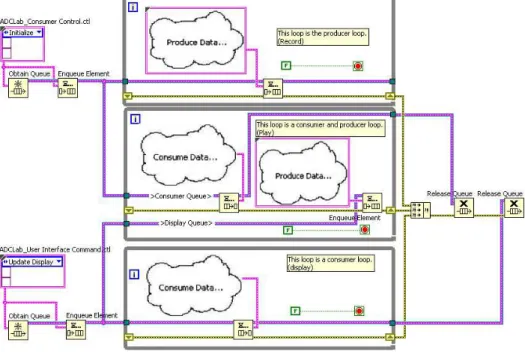
The ADCLab tool is an implementation of the so called “producer-consumer” loop technique [8], which allows managing data collection and analysis in parallel loops and fits well with the use model of lab data acquisition and their simultaneous analysis.
Three loops have been designed following the sequence “Record-Play-Display”. “Record” implements the parameter setup phase allowing the user to enter the typical test conditions and eventually prepare the data acquisition phase, “Play” runs the model simulation (or acquires the data) and analyze the data, “display” opens the display dialog box and provides the various graphs and numerical results.
In these architectures queues are used to communicate between the loops and synchronize their execution. Figure 1.1 gives an abstract view of the queuing mechanism.
The “ADCLab Consumer Control” queue gets initialized at the run, then starts queuing data (responding to user commands) into the panel setup and communicates with the consume section of the second loop. The second loop plays the simulation and at the same time acts as producer of the output data to be delivered to the display loop. The communication between the second and third
3 loop is implemented by the “ADCLab User Interface Command” queue in a similar manner as the previously described one. Finally both queues are released responding to the “exit” command given by the user.
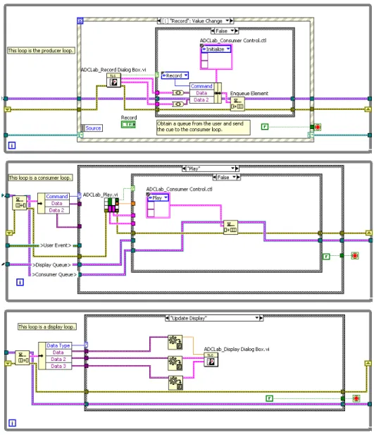
LabVIEW programs and subroutines are called for historical reasons (even when not interfacing directly to any instrument) virtual instruments (VIs). The Figure 1.2 depicts the structure of the three loops in more detail highlighting for each loop the main “.vi” files used.
The “Record” loop is driven by the “ADCLab_Record Dialog Box.vi”, the “Play” loop by the “ADCLab_Play.vi” and the “Display” loop by the “ADCLab_Display Dialog Box.vi” .
Figure 1.1: Abstract of the queuing mechanism used for the communication and synchronization of the loops
Additionally to the main ADCLab project tool, a panel has been developed to guide through the architectural choice consisting of 4 main sections.
A “setup and simulation” phase allows inputting the main characteristics wanted for the ADCs and for the stimuli tone(s), like the sampling frequency, the bandwidth, and the number of output bits in the case of multi-bits structures. A tab named “Noise Shaping Design” brings the user through the choice of the noise filter (and as consequence, of the Loop filter too) characteristics like topology (e.g. Butterworth, Cheybischev, etc.) and the bandwidth of the filter. From the noise shaping parameters the characteristics for the open loop and closed loop filters, are determined, the stability is analyzed, and the coefficients of an IIR implementation are calculated in the Frequency Responses tab.
5
1.3 Shaping of Transfer function
1.3.1 Noise shaping
Through the “Noise shaping” panel the quantization noise projection over the bandwidth of interest will be setup. We assume the model reported in Figure 1.3 and the input/output definition highlighted at Figure 1.4. The noise shaping (NS) - loop filter (H) relation expressed by:
H
k
∗
+
=
1
1
NS
(1.1)Considering a discrete time implementation, the panel will include a number of topologies for the filter, including Butterworth and Inverse Cheybischev ones. The following example shows the Butterworth case for a 3rd order loop filter featuring a 6 MHz sampling frequency and a maximum input bandwidth at 24 kHz.
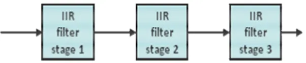
The implementation of the noise filter is modeled as an Infinite Impulse Response (IIR) cascade filter, with each stage modeled as 2nd or 4th order IIR filter (see Figure 1.5).
Figure 1.5: Noise shaping in a cascade IIR form
Figure 1.4: input and output for calculation of the quantization noise transfer function
In terms of transfer function the resulting NS(z) can be written as a product of smaller order stages, which is referred in the tool as “cascade form” or in a more classical “direct form”. In both cases “a” coefficients will be referred as “reverse coefficients” while the “b” coefficients will be indicated as “forward” coefficients. Below the general equation for a cascade form (series of second order stages):
∏
= − − − −+
+
+
+
=
Nst K k k k k kz
a
z
a
z
b
z
b
b
z
NS
1 2 2 1 1 2 2 1 1 0*
*
1
*
*
)
(
(1.2)and the general equation of direct form
na) < (nb 1 1 1 1 1 1 0
*
...
*
1
*
...
*
)
(
− − + + − −+
+
+
+
+
+
=
na na nb nbz
a
z
a
z
b
z
b
b
z
NS
(1.3)An important consideration applies to this function. The causality of the systems implies a delay of at least one element [9]. This means that the denominator order of H must be higher than the numerator order. In other terms given from (1.1):
)
(
)
(
1
1
)
(
z
NS
z
NS
k
z
H
=
∗
−
(1.4)The numerator of 1-NS(z) must be at least one order less than numerator of NS(z). To comply with this condition coefficient b0 in (1.3) must be 1 so that H(z) is represented by:
)
*
...
*
(
*
*
...
*
)
(
...
*
)
(
)
1
(
1 1 1 0 1 1 1 1 1 0 + − − + − + − −+
+
+
+
−
+
−
+
−
nb nb na na nb nb nbz
b
z
b
b
k
z
a
z
b
a
z
b
a
b
(1.5)if b0=1 the numerator order of H(z) will be reduced by one with respect to the denominator. By comparing (1.2) and (1.3), it could be sufficient to add to the first
stage of the Noise shaping cascade IIR filter a gain of 1/b0. This operation will be
referred as weighting in the document and in the LabVIEW™ panel.
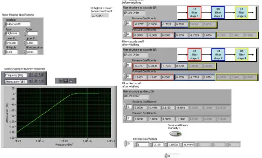
In the proposed example and assuming a corner frequency of 240 kHz (placed one decade over the desired signal conversion bandwidth), the coefficients in Figure 1.6 have been obtained. From top to bottom in the picture the coefficients represent respectively the equation (1.2) before and after weighting and the equation (1.3) after weighting. In particular it can be noticed that forward coefficient b0 (in the direct form) is now 1 as expected. At the bottom the possibility to input coefficients manually is given, to allow an easy comparison with coefficients from previous designs, obtained with other tools, or for a custom tuning of the noise shaping transfer function.
7
1.3.2 Open and Closed Loop Frequency responses
The OLF (Open Loop Frequency response) and CLF (Closed Loop Frequency response) are then plotted in the next panel (Figure 1.7). Through this panel the , where DC gain, poles and zeros of the open loop and closed loop transfer functions can be checked.
Figure 1.7: Open loop and closed loop plots and coefficients Figure 1.6: Noise shaping panel
1.4 Stability checks
To prove that the set of coefficients determined will result in a stable closed loop system the “stability check” panel tab has been implemented, which plots the root locus function and finds the minimum value of the feedback gain K (see Figure 1.3). The stability panel (Figure 1.8) shows that for K>0.04 the closed loop poles fall inside the unit circle.
1.5 Setup and simulation panel
To build a testbench setup, the sampling frequency and the testing signal frequencies have to be fixed first. The number of samples should be a power of 2 and the number of cycles in the DFT window must be an integer. If for fs=”sampling frequency” and fin=”input frequency“, N=”number of samples” and Np=”Number of periods” in the fft the following conditions are respected:
N=”power of 2”,
Np=”prime integer number”, fs/fin=”N/Np”,
the DFT is coherent. This guarantees, together with the application of a windowing function (the tool let the choice between a number of different weighting functions) minimum leakage in the power output spectrum.
Up to now the real circuit implementation did not play a role in the analysis. Summarizing, the parameters of the noise shaping function have been chosen, the open loop and closed loop coefficients have been derived, stability has been checked and the results are now being verified through a test-bench setup as shown in Figure 1.9.
9 To effectively test our set of coefficients an idea of the circuit noise we are expecting in our implementation is needed. Normally the expected resolution of the converter is given as a specification item in terms of number of “resolution bits” of an equivalent Nyquist converter. The problem can be easily reversed.
We may use the well known relationship between SNR (signal to noise ratio) and resolution bits (N):
SNR [dB] = 6.02N + 1.76 (1.6)
The noise in the SNR is the sum of the quantization noise generated by the sampling activity of the modulator and the circuit noise introduced by the electronic components. Targeting for instance an area optimized architecture the quantization noise in band should be negligible with respect to circuit noise. Hence as a starting
point we can assume, that for the specified N for a reference full scale of 1 V (1VFS)
and for a sampling frequency fs the rms noise voltage in the specified bandwidth (BW) is:
BW
fs
V
Vn
SNRdB FS rms•
•
=
−2
10
1
20 ] [ (1.7)this is referred as: “circuit noise (Vrms)” in Figure 1.9. The tool will only require as an input the desired resolution in bits in the “Equivalent resolution Spec (bits)” field
(13 bits in the example aiming to achieve an 80 dB SNR). A 1.115e-3 Vrms input
referred noise will be added to the test signal to account for the maximum tolerable circuit noise hence emulating a worst case test bench setting. If the chosen set of coefficients will still show a 80 dB (or, like in the example, 60 dB with -20dB input
amplitude) the next phase will be the mapping of the coefficients to one of the available architectures (feed forward or feed backward in the audio converter case [10] and/or multi-bit architectures in the case of large bandwidth [11] otherwise other options can be tried out, like changing the noise shaping filter transfer function by increasing the filter corner frequency or increase the order of the filter.
1.6 Application examples
1.6.1 Audio ADC
As an example we design a sigma-delta ADC with a resolution of 16ENOB at a sampling frequency (fs) of 10 MHz and a conversion bandwidth (BW) of up to 20 kHz.
The first step consist of finding the minimum order for the ADC loop filter required to achieve the spec as a function of the OSR (over sampling ratio).
The theoretical minimum order required can be found in literature. The signal-to-noise ratio (SNR) vs. oversampling ratio (OSR) of a single-bit sigma-delta modulator is shown in Figure 1.10.
In the case of our example OSR = (fs/2*BW) = 250 and 16 bit corresponds to 98 dB dynamic range. From the graph the minimum required order for a single bit converter would be between 2 and 3 as highlighted in Figure 1.11.
Figure 1.11: Back-annotated for OSR=250 SNR=98
Figure 1.10: Maximum SNR achievable by modulators of order n with coincident zeros, as a function of oversampling ratio [10]
11 In the tool we might input 16 bit in the equivalent resolution spec field at the “Setup” panel, then use the “filter coefficient” model to find the loop filter coefficient. In the noise shaping panel we might start with an order of 2 and a Butterworth high pass filter shape setting the corner frequency (fc) of the filter at 2 decades above the required signal bandwidth. This would mean 2 MHz in our example.
By running the noise shaping panel and then the frequency response panel we get the coefficients and by returning to the setup panel we might find out, if the required SNR has been achieved and also by means of the stability panel, if the conditions for stability are fulfilled. If stability is not reached one could decrease the corner frequency of the filter, if SNR is too low we have to increase the order of the filter.
As a guideline we might define the flow as described in Figure 1.12, where it has also been considered that when the SNR obtained by the simulation is slightly higher with respect to the spec one solution could also be the reduction of the input noise in the input test signal which moves the effort in try to reduce the circuit noise. This noise is in fact the maximum input noise the architecture will tolerate to be within the spec and it is good practise to have it of the same order of the maximum tolerable quantization noise. This will allow a good tradeoff between area and performance. In case the result of the model is close to the spec, the increase of the order might anyhow result in a much higher area penalty in design than limiting the circuit noise by increasing the size of the circuit parameters (capacitor area,currents..etc) . For this reason the flow considers the case “SNR achieved = NEAR” in Figure 1.12 as a special one.
In chapter 2 the refinement of the coefficients will be treated in the particular example of the audio ADC design.
1.6.2 Large bandwidth ADC
Example for a design of a sigma-delta ADC with 13 ENOB resolution at a sampling frequency of 640 MHz and a conversion bandwidth of up to 10 MHz.
Referring to Figure 1.10 we will notice, that in this case the required resolution will not be feasible with a low order architecture, and we must also consider that for systems with orders higher than 6 it is practically impossible to get a stable delta-sigma closed loop.
Figure 1.13: back-annotated Figure 1.10 for OSR=32 SNR=32 Figure 1.12: Architecture choice flow
13 To cope with this problem a dedicated panel has been developed in the tool which implements a Multi-stAge noise SHaping (MASH) ADC architecture.
By implementing the diagram of Figure 1.14 one can take advantage of several architectural solutions (cancellation of quantization noise via its re-sampling in a parallel loop, usage of flash N bits ADC) at the cost of increased complexity.
Each bit of depth of the FLASH ADC corresponds to circa 6 dB of saving in the required resolution of the delta-sigma loop. For instance in the case of our example by using a FLASH ADC with 3 bits output we can lower the required maximum SNR of the loop filter up to 80-(3*6)=62 dB, hence ending up (referring to the blue
line on Figure 1.13), in a solution which is feasible by using a 3rd or 4th order loop
filter. Considering the parallel loops in Figure 1.14 it might be convenient to design
two identical 2nd order loop filters and re-use them to build a 4th order system. It
must be noticed that the loop in the dashed rectangle in Figure 1.14 is different from the one adopted for the audio bandwidth case because it contains the feed forward of the input to the adder, which allows to get the quantization noise of the first loop as an additional output to be re-sampled in the second loop. This transfer function is also implemented in the tool and will be activated by switching from the “Audio Setup” to the “HBW Setup” tab in Figure 1.9.
The rest of the flow to tune the loop filter coefficients will be identical to the one described by Figure 1.12.
2. ARCHITECTURES MAPPING INTO DESIGN
2.1 Introduction
Once the coefficients of the filters and of the integrators are found they still need to be mapped into the design. This chapter will analyze our examples for audio and for wide bandwidth applications and will report the result of the model simulations.
2.2 Architecture mapping
Two main classes of architecture are widely adopted for delta-sigma loops. The distinction is based on the control loop feedback being derived as a weighted sum of the integrator outputs (feed forward architecture) or as the main output fed back to each integrator input (feed back architecture).
Both choices are suitable to implement the coefficients derived in chapter 1 and the labVIEW tool implemented does not assume a particular structure when finding the loop filter coefficients.
2.2.1 Audio bandwidth ADC example
The equation (1.5) together with the causality condition b0 = 1 (see Section 1.3.1)
will be mapped hereby to an architecture with feed forward coefficients for a 3rd order loop depicted in Figure 2.1
In the tool, mapping the coefficients in the feed forward case consists of writing down the equations for the forward coefficients of the open loop transfer function and comparing the result to the numerator of the general transfer function obtained for the 6th order case (maximum order implemented in the tool). The numerator of Eq.(1.5) will be represented by :
6 6 5 4 3 2 1 5 5 4 3 2 1 2 4 4 3 2 1 3 3 3 2 1 4 2 2 1 5 1 1
)
1
(
)
1
(
)
1
(
)
1
(
)
1
(
f
k
k
k
k
k
k
z
f
k
k
k
k
k
z
f
k
k
k
k
z
f
k
k
k
z
f
k
k
z
f
k
+
−
+
−
+
−
+
−
+
−
(2.1) An example for the 3rd order case when the numerator of the OL (open loop) transfer function will be the following:3 3 2 1 2 2 1 2 1 1
f
(
z
1
)
k
k
f
(
z
1
)
k
k
k
f
k
−
+
−
+
(2.2)15
Considering that k1 multiplies the entire numerator expression, we may take it as a
gain factor and naming c1, c2 and c3 respectively the 2nd , 1st and 0 order
coefficient of the Eq. (2.2), the following set of equations will be extracted:
1 1
c
f
=
(2.3) 2 1 2 2f
2
f
c
k
−
=
(2.4) 3 1 2 2 3 3 2k
f
k
f
f
c
k
−
+
=
(2.5)The three equations are featuring five variables so that two more constraints are needed. The first constraint could come from the implementation of the feed forward coefficient. We need then a deeper look at a possible implementation of the adder in Figure 2.1. A typical implementation in a switched capacitor form is represented in Figure 2.2, where ph1 and ph2 represent two opposite clock phases
for ph2=H and ph1=L (first capacitor is shorted) the sum of the total charge at the three capacitors can be written as :
2 2 3 3 3 2 1
Q
Q
0
C
V
C
V
Q
+
+
=
−
−
(2.6)for ph2=L and ph1=H (C2 and C3 in parallel with one terminal to the virtual ground, C1 is charging): sum sum sum
C
V
C
V
V
V
C
Q
Q
Q
1+
2+
3=
1(
1−
)
−
2−
3 (2.7)Considering that the charge must be preserved in the process we get :
sum sum sum
C
V
C
V
V
V
C
V
C
V
C
3 3−
2 2=
1(
1−
)
−
2−
3−
(2.8) and : 3 2 1 3 3 2 2 1 1C
C
C
V
C
V
C
V
C
V
sum+
+
+
+
=
(2.9)As the adder is formed by a ratio of passive components (fx= Cx/(C1+C2+C3)) the
sum of the three coefficients will result in being equal to 1. Because the comparator after the adder is sensitive only to the sign of the sum, coefficients f3, f2, f1 can be
scaled down, ) even if, due to other constraints, some of the coefficients are greater than 1 the sign of the sum will not be affected by a multiplication factor. Based on these considerations the 4th constraint can be expressed as:
0 <
f
1,
f
2,
f
3<
1
U
f
3+
f
2+
f
1=
1
(2.10)Assuming a switched capacitor implementation of the integrators like the one in Figure 2.3
and fs = sampling clock frequency, the integrator coefficients (kx in the set of
equations) will be Cs/Cfb. Sampling and integrating caps (Cs, Cfb) cover a
considerable part of the integrators area. As Cfb mainly depends on the sampling
frequency, the size of the circuit can be reduced by minimizing Cs. The lower limit
for Cs minimization is set by noise requirements as discussed in [3].
Cs values are directly proportional to Kx as described in Figure 1.3 so minimizing
the sum K2 + K3 will minimize the circuit area of the capacitors.
From equations (2.3), (2.4), (2.5), (2.10) it is easy to verify that K2 and K3 depend
only on f2 , if c1, c2, and c3 are known.
1 2 2 2
f
c
2c
k
=
+
(2.11) 3 1 2 2 1 2 3 2k
(
1
f
c
)
k
f
c
c
k
−
−
−
+
=
(2.12)This translates into a further constraint:
)
(
)
(
min(
2 2 3 2 2K
f
K
f
f
→
+
) (2.13)∫
−
=
V
t
dt
C
s
fC
t
V
s fb out1
(
)
1
)
(
or in the time step ∆t=1/fs , kx= Cs/Cfb
∫
∆ +∆
−
=
∆
t t t s x outV
t
dt
t
k
V
(
)
17 An equation solver implemented in the tool for the 3rd order case allows us to solve the equations and back-annotate the coefficients in the model. At the setup panel with a mouse click on the model selector field the resulting power spectra for the chosen model will be plotted and SNR calculated.
The upper section of Figure 2.4 implements the expressions of (2.11) and (2.12), the “Build text” express VI builds the expression of (2.13), and the “Find all Minima”
.vi finally finds the f2 value corresponding to the minimum of that expression and
feeds back the value to recalculate the other kx and fx coefficients.
2.2.2 Large bandwidth ADC case
A Multi-stAge noise SHaping (MASH) architecture has been implemented in the tool to support the multi-loop sigma-delta concept [11],[12],[13].
The structure has been described in Section 1.6.2 and the maximum order of the noise shaping filter in the tool is set to 3 for each loop filter in this architecture - hence having 2 loops the total order of the modulator will be 6.
The Labview™ tool setup panel allows to choose the depth (number of bits) of the FLASH converter (and of the DAC).
Once this has been done, the architecture mapping problem consists of finding the correspondence between the coefficients found by the tool and the equation of the loop filter H in Figure 1.14.
Hereby an example for a 2nd order loop filter which corresponds to a 4th order
MASH architecture. The numerator of the filter in the feed forward architecture is :
2 2 1 1 1
f
(
z
1
)
k
k
f
k
−
+
(2.14)A flow similar to the one described in Section 2.2.1 can be applied.
Figure 3.5: Model simulation of a 3rd order Butterworth architecture obtained via the flow and the solver described in Chapter 2(1.5)(1.5)(1.5)
19 We assume a sampling frequency of 160 MHz with a 10 MHz bandwidth (as required from the WLAN standard) for an OSR = 8.
The implemented model for a second order noise shaper filter includes a solver block to calculate the coefficients similarly to what was shown in Figure 2.4. Figure 2.6 shows the spectrum for a MASH architecture featuring a 3 bit flash
ADC/DAC. The set of coefficients for the ADC proposed in [11] (k1=0.5, k2=0.5,
f1=4, f2=4) has been replaced by a set found by the flow and mapped by the tool
described in this paper (k1=0.50, k2=0.50, f1=4.83, f2=6.47). The two model
configurations have been simulated and compared by simulations. The set of coefficients found shows a maximum DR of 81.3 dB when setting the max input
referred noise to 0.107 mVrms (in the 10 MHz band). If we use the coefficients of
[11] we 74 dB get instead. As the difference is more than 6dB we can reduce the output ADC/DAC’s resolution to 3 bits instead of 4 (see Figure 5) allowing a large reduction of the DAC area on silicon die, and still get 69.4 dB. So the results are comparable to the DR claimed in [11] (69.1 dB) but with at reduced area.
Figure 2.6: MASH delta sigma ADC, power spectrum, -10dB input signal @ 1.24 MHz, 3 bit resolution output DAC
3. PWM GAIN CONTROL TECHNIQUE IN A DELTA-SIGMA
AUDIO ADC FOR MOBILE APPLICATION
3.1 Introduction
A standard application for an Audio ADC is the conversion of signals coming from the microphone of a mobile telephone into digital bit-streams, which are processed by the DSP for further transmission via the radio part.
In our case we call the chain of functional blocks, which produce the bit-stream starting from the “weak” microphone signal “audio uplink” or “audio transmit” path. Several signal adaptations are required before sending it to the ADC. In this chapter, following a general introduction of the uplink path, a technique to embed the gain control inside the delta sigma ADC loop will be described.
3.2 Mobile telephone uplink path
The next figure shows a simplified block diagram of an uplink path
We can extract the following chain of electrical building blocks (from left to right in the continuous line rectangle at Figure 3.1 ) :
Microphone interface (embedded in PreAmp in the picture) → Preamplifier →
Programmable Gain Amplifier (PGA) → ADC
Additionally a reference generator is required to provide the correct reference voltages and bias currents to the ADC and a Zero Crossing Detector (ZCD). Since the gain change can cause plop or click noise in audio systems [14], the ZCD will detect the zero crossing of the input signal and will allow the gain switching only when the signal amplitude is very close or equal to zero. with minimum impact on the audibility of this change. This technique provides a significant reduction of the audio noise and reduces one of the sources of non-linear distortion in the sound processing, where most of the evaluations are subjective and complex [15].
3.3 Uplink path: from microphone interface to the ADC input
Figure 3.2 shows two typical microphone interfaces. The microphones get biased from the integrated circuit by the Vmic_bias block and the microphone currents arecollected through a 2kΩ resistor in the chip. This interface requires the 3 external
capacitors while all the rest is integrated in the silicon.
21 On the left the external microphone interface has two dedicated pads to detect the insertion of the external microphone which will enable the biasing of the microphone through the Vmic_bias buffer.
The signal collected at the Ext_mic or Int_mic pads will then get amplified and shifted around a common mode voltage to allow a differential interface at the Programmable Gain Amplifier or at the Audio ADC input.
The preamplifier is a low noise differential amplifier which adjusts the gain to cope with the different use modes of the uplink path such as the analogue loop back of the receive path (earphone or headset paths) through feedback resistors used in stereo FM recording, the DC offset calibration of the earphone amplifier through diagnostic lines (diag1, diag2), and of course the internal and external microphones modes.
The microphone interface and the preamplifier are followed by a PGA , which adapts the gain according to the requirements (for example if the user changes volume or for automatically adapting to the quality of the communication environment).
In the following sections a solution will be described to embed the PGA functionality in the delta-sigma ADC.
3.3 Gain control in the audio uplink path for mobile applications
3.3.1 The glitch-free gain switching method
The ADC described in this chapter adopts a 1-bit feed-forward third-order switched-cap sigma-delta architecture as shown in Figure 3.3 .
It has been modelled and tuned as described in [22].Assuming dithering and offset are not yet inserted, the resulting signal transfer functions for open loop (3.1) and closed loop (3.2) are:
{
}
1 3 3 ) 2 ( ) ( 2 3 2 1 1 2 2 2 2 3 3 1)
(
− ⋅ + − ⋅ + ⋅ − ⋅ + ⋅ − ⋅ +=
z z z z s z s g s g s s g sz
H
(3.1))
(
1
)
(
)
(
)
(
1z
H
g
z
H
g
z
Vin
z
Vout
ref⋅
+
⋅
=
(3.2)where g1, g2, g3, gref represent the integrators and DAC coefficients, given by the
ratios between sampling and integrating capacitor, while s1, s2, s3 are the ratios
between the respective capacitors in the adder and their sum.
Assuming by design a flat H(z) in the band of interest we define H0 as the low
frequency gain and design gref *H0 >> 1. Hence the overall gain of the system can
be written as: ref ADC
g
g
Gain
=
1 (3.3)The coefficient gref is implemented by two capacitors and two switches, as shown
in Figure 3. It allows us to set the overall gain by changing the feedback coefficient
of the filter. An appropriate value for gref can be selected by adopting a bank of N
capacitors in parallel controlled by a binary switching algorithm as shown in Figure 3.4. The coefficients are realized by means of metal-oxide-metal (MOM) capacitors. The gain expressed in (3.3) only depends on the ratio of two MOM capacitors, which can be implemented with very good reliability and robustness with respect to process and temperature variation.
1 1 2 1 − − − ∗ z z g 1 1 3 1 − − − ∗ z z g 1 1 1 − − −z z 1 g s3 2 s 1 s in V dt s os g ref g ) (z H dith n Q out b 1 ) (Vout os
Figure 3.3. ADC block diagram with offset (os) and dithering (dith) insertion.(the dashed line encloses the Open Loop section).
23 Figure 3.5 shows the two non-overlapping clock phases (ph1 and ph2) of the schematic circuit in Fig. 3 and the time separation between two edges of the
phases. When ph2 is high and ph1 is low, the capacitors Crefn, Crefp Cin and Cip
have one terminal connected to Vcm. Thus, they sample the input or reference
voltage values with respect to the common mode voltage (Vcm.) , while the
integrating section is holding the previous voltage values. In the next phase, ph2 is low, ph1 is high, and the connections to the reference capacitors are swapped at the same time as the connections to the input capacitors. The integrator section is now connected to the input sampling section and it integrates the differential voltage values sampled in the previous phase. Equation (5), which is based on the principle of charge conservation, reports the voltage at one input of the integrator
(Va) highlighting the sum between the input and reference voltages, under the
simplifying assumptions that Vcm = 0, data is high, datan is low and that the
integration on Cfp and Cfn has not started yet.
)
(
*
)
(
*
*
V
inpV
refnC
refpC
ipV
innV
aC
refpV
refpV
aCip
+
=
−
+
−
(3.4) refp ip refp refn refp ip inp inn aC
C
V
V
C
C
V
V
V
+
−
−
−
=
(
)
(
)
(3.5) ph2 ph2Figure 3.4 Implementation details for the gref coefficient and gain-switching
capacitors (ph1 and ph2 are two non-overlapping complementary clock phases, data
and datan are complementary output data feedback paths). Vcm is the common mode
The single capacitors used for implementing the total capacitanceCref are sized according to a binary weighted function and their possible combinations allow the implementation of a large number of possible values. 11 possible gain settings have been chosen for the silicon implementation of the case study reported
hereinafter in Chapter 5. 4 4 gain control bits are necessary to set up the proper
combinations of binary weighted capacitors resulting in the values listed in Table 3.1.
Table. 3.1. Capacitor selection: the decoding and switching table
Each step between the 11 settings corresponds to a gain change of 2dB.
In order to smooth the transition and its unwanted audible effects, a switching algorithm applying the PWM (Pulse Width Modulation) technique to each gain change is realized as shown in Figure. 3.6. This is possible because of the low rate of the gain change compared to the ADC clocking frequency.
decoded gain-set gain-set gain-set gain-set gain-set gain-set gain-set bits → <0> <1> <2> <3> <4> <5> <6> always
binary weights (in number of unit caps)
on ↓ 1 0.125 0.25 0.5 1 2 4 8 total unit caps ↓ ON ON ON ON 12 ON ON ON 9.5 ON ON ON ON ON 7.63 ON ON ON 6 ON ON ON ON ON 4.75 ON ON ON ON 3.75 ON ON 3 ON ON ON ON 2.38 ON ON ON ON 1.88 ON ON 1.5 ON ON 1.25
25 The driving signal of the capacitor switches allows the duty-cycle to change linearly from 0 to 1 over the transition time T, while the gain is slowly switched in 2 dB steps. The improvement achieved by this switching method is clearly visible on the plots of the reconstructed waveforms Figure. 3.7 (a) and (b), showing the comparison between the two cases (with and without PWM technique).
3.3.2 Parameters tuning for gain switching
Figure. 3.8 shows a possible implementation for the digital gain control of the ADC, when the PWM is applied to the step change.
Amplitude 80% -80% -60% -40% -20% 0% 20% 40% 60% Time (ms) 10 0 2 4 6 8 Amplitude 80% -80% -60% -40% -20% 0% 20% 40% 60% Time (ms) 10 0 2 4 6 8 (a) (b)
Figure. 3.7. . Comparison of the reconstructed waveforms of a 0.1 V input
sine wave at 5 kHz for staircase gain switching (simulation): (a) without PWM; (b) with PWM. t0 t1 t2 t3 t4 t5 t6 t7 t8 t9 t10 → ∆t ← G a in , G (d B ) Time G a in , G (d B ) gn=g0+2 go ∆ ∆∆ ∆t T ti Time tT ti+1 (a) (b)
Figure. 3.6. PWM gain switching implementation example: (a) Staircase gain switching, stepping from 0 to 20 dB settings; (b) enlargement of one step
The multiplexer output selects alternatively go (previous gain selection) gn (current gain selection) at the pace determined by the output of the “PWM 128” block. This block is a 7 bit counter, which continuously runs. If the count value is lower than its duty input, then it outputs 1 else 0. The “7b counter” block counts from 0 to 127 and its output is driving the PWM duty input. The “=127” block is a comparator set with 127. When this condition is reached, the new gain selection signal is stored for the next switching step. The ramp duration can be set using the “ramp duration (T)” signal, whereas its frequency is determined by the division of the master clock frequency by the factor “PWM freq”. The “Run ctrl” block is a simple state machine providing the start and reset signals to the system.
The behavior of the gain control circuit is determined by a number of parameters such as:
clock frequency = sampling frequency (fs) of the ADC (5 MHz in the case study);
T = transition duration; determines the duration of the gain transition (a ramp in the example);
ginit = gain value at the gain ramp start (in the range from 0 to 20 dB in minimum
steps of 2 dB);
gfin = gain value at the gain ramp end (in the range from 0 to20 dB in minimum
steps of 2 dB);
go = previous gain selection (in the range from 0 to 20 dB in minimum steps of
2 dB);
gn = current gain selection (in the range from 0 to20 dB in minimum steps of
2 dB);
Npwm = Number of PWM pulses (128 in the example).
If we assume a 2 dB minimum step size, the following relations hold (6)-(8):
steps n fin g init g ition gain trans a in steps db 2 of number 2 = = − (3.6)
Figure. 3.8 . Simplified block diagram of the ADC circuit with PWM-controlled
27 2 * ns T f steps s
n
=numberofclockcycles ina2dbstep= (3.7)2
1<Npwm <ns (3.8)
Two implementation options are possible based on the previous relationships:
1) set the transition time T, calculate ns2 and choose Npwm in the given range;
2) set ns2, calculate transition time T and choose Npwm in the given range.
Option 1 may be preferable at system level, as gain transitions will have a uniform duration. It should also be considered that a transition time which is long enough to smoothen the transition and a sufficient number of PWM pulses are needed to get the best benefits of the PWM switching technique.
The transition time for gain change is not a critical parameter, as the rate of the gain change signal is very low (normally below 10 kHz) in typical audio
applications. However, the value of Npwm is programmable in the silicon design of
the case study, so that the best settings can be found during the validation phase.
The impact of the Npwm value on the position of spurious signals during the gain
transition can be proven by simulations. The Discrete Fourier Transform (DFT) of the output signal reveals the onset of spurious components in the frequency band of interest. Figure 8 shows two simulation results featuring the DFT of the output when a sine wave at 5 kHz with 0.1 V amplitude is sampled at 5 MHz. The gain is
switched from 0 to 10 dB in 10 ms for two different values of Npwm. 50,000 samples
have been acquired to cover the complete transition. Note that the maximum value
of Npwm = ns2 is 1200 clock cycles in this case.
Finally, it should be noted that the gain changing technique modifies the ADC transfer function in the desired way, but it also affects the dithering and offset paths, leading to an amplification of their effects.
dB -3 -120 -110 -100 -90 -80 -70 -60 -50 -40 -30 -20 -10 frequency 3E+6 100 1000 10000 100000 1E+6 Npwm=100 spurious tone 54.84 kHz ↓ dB -3 -120 -110 -100 -90 -80 -70 -60 -50 -40 -30 -20 -10 frequency 3E+6 100 1000 10000 100000 1E+6 Npwm=200 spurious tone 24.92 kHz ↓ (a) (b)
Figure. 3.9 PWM modulated gain transition output spectra for two Npwm values
(model simulation): (a) Npwm = 100 PWM gain transition showing spurious at
54.84 kHz; (b) Npwm = 200, spurious appears at 24.92 kHz approaching the audible
4. DITHERING AND OFFSET INSERTION IN A VARIABLE GAIN
LOOP
4.1 Introduction
Idle-tone shifting by dithering or DC-offset is often applied to mitigate the nonlinear errors due to the quantization and statistical DC offset. The quantization error results in an input dependant noise which might be disturbing form a psychoacoustic perspective and is normally quite difficult to reduce. Depending on its amplitude the offset can introduce an idle tone which might be falling in the audible band. The techniques adopted to cope with these issues are normally the introduction of a dithering signal and/or of an additional offset. The gain control in the feedback loop described in the previous chapter must then account for the impact on dithering and idle tone shifting too. Hereafter possible solutions applied to the case- study proposed in chapter 3 will be discussed.
4.2
Dithering concept
The quantization error resulting from an ideal PCM modulation is generally considered a white spectrum noise [16]. This is only valid under the conditions that the input signal amplitude is much higher than the quantization step size and its frequency content is uncorrelated to the sample frequency Deviation from these two conditions can lead to artefacts [17][18]
Adding to the input of the quantizer a dithering signal featuring a triangular probability distribution (TPD) and amplitude equal to the step of the quantizer will make the quantization error noise independent from the characteristics of the input signals at the penalty of an increased noise floor and stability weaknesses [17], [19].
As shown in [17], it is possible to achieve idle tone suppression by using a dither signal with a rectangular probability distribution function spanning ± 0.5 LSB (half bit of the quantizer output range). Figure. 4.1 shows the simulation results of the dithering effect. The un-dithered spectrum shows idle tones in the audible band when a 1 mV DC offset is applied at the input. The spectra after dithering show much reduced impact of the offset on the quality of the output.
dB 0 -180 -160 -140 -120 -100 -80 -60 -40 -20 frequency 3E+6 100 1000 10000 100000 1E+6
undithered power spectrum
idle tones (1mV DC input offset)
dB 0 -180 -160 -140 -120 -100 -80 -60 -40 -20 frequency 3E+6 100 1000 10000 100000 1E+6
dithered power spectrum
(b) (b)
Figure. 4.1 Effect of dithering on the idle channel power spectrum plots with 1 mV DC input offset. (simulation): (a) undithered ; (b) dithered.
29 To prevent a possible modulator output saturation when dithering is applied a tuning of the dithering based on the output amplitude can be applied.
By monitoring the output signal, it is possible to detect when the output is reaching the saturation limit and to prevent the dithering insertion in large signal conditions. This monitor has been implemented by a digital filter that collects four consecutive output samples and disables dithering if two equal samples out of the last four are
detected (see Figure. 4.2).
4.2
Dithering in a variable gain delta sigma loop
The gain regulation in the feedback loop as proposed here poses another challenge. Increasing the gain also amplifies the dithering input and its drawbacks. The effect on the noise will be hardly noticeable because of the general increase in noise floor during a gain increase. In high gain conditions, the dithering might
cause the system saturation and even if the filter of Figure. 4.2operates to prevent
the output saturation, an incorrect behavior may occur because of the possible oscillation of the “dither disable” filter output. To quantify this effect, different gain conditions have been simulated in a Labview™ model of the system.
Table 4.1 shows the maximum dithering levels allowed, their rms values for each gain setting and their associated maximum input level. The reduction of spurious tones in the spectrum is a function of the rms value of the dithering signal. A set of 9 different coefficients would be required for a full implementation of the proposed strategy. However, if we observe the rms values (hence the power) of the dithering signal of Table 4.1, , we note that the dithering power never falls below the value obtained for gain 0, when the gain ranges from 0 to 10 dB. Thus, we are able to cover a range from 0 to 10 dB without performance degradation in terms of idle tone suppression with respect to the nominal case (0 dB gain), by just realizing one coefficient. For the remaining range (from 12 to 20 dB) a full set of coefficients would be required instead. In the fabricated silicon chip a tradeoff between performance and complexity has been considered and only the minimum values in each of the two mentioned intervals have been implemented. In particular, we used a value of 0.25 LSB in the range from 14 to 20 dB and 0.57 LSB in the range from 0 to 12 dB, as indicated by the grey rows of Table 4.1.
4.3
Idle tone shifting by offset insertion
Unavoidable idle tones are typical for delta-sigma systems. Adding a small offset in the input path of the ADC allows the idle tones to be shifted outside of the band of interest (from 20 Hz to 24 kHz for high quality audio applications).
An input-referred DC offset will produce an idle tone at the frequency given by [20]: s f G out V off V it f = ⋅ ADC⋅ FS IR (4.1)
where fit is the frequency of the idle tone, VoffIR is the input referred DC offset, VoutFS
is the full scale output voltage, GADC is the ADC gain and fs is the sampling
frequency. Considering fs = 5 MHz, a 5 mV offset leads to the onset of an idle tone
with fit = 25 kHz. A 3.75% (with respect to a 1 V full scale) systematic offset has
thus been added to shift the possible idle tones. This causes the idle tones to shift up to more than 1 decade over the bandwidth limit when no gain is applied
(GADC = 1).
Unfortunately, the gain applied to the converter feedback results in an offset increase by the same amount as for the input signal. For instance, applying a 20 dB gain setting results in the output offset being increased from 3.75% to 37.5% and this will cause an unacceptable limitation of the output dynamic range. The solution to this problem is to embed the offset input inside the gain control and to use the same set of switches and binary weights to find the best matching values
of gref. Therefore, the block scheme of the system is modified as described in
Figure. 4.3:
gain settings (dB)
max input level (V) max dithering Level rms dithering (FS condition) 20 0.1 0.25 0.07 ← ←← ← implemented 18 0.126 0.34 0.1 16 0.158 0.41 0.12 14 0.2 0.49 0.14 12 0.251 0.57 0.17 10 0.316 0.65 0.19 8 0.398 0.78 0.23 6 0.501 0.84 0.26 4 0.631 0.84 0.26 2 0.794 0.8 0.26 0 1 0.57 0.19 ← ←← ← implemented
![Figure 1.10: Maximum SNR achievable by modulators of order n with coincident zeros, as a function of oversampling ratio [10]](https://thumb-eu.123doks.com/thumbv2/123dokorg/7572959.111776/17.723.218.507.693.873/figure-maximum-achievable-modulators-order-coincident-function-oversampling.webp)