2018
Publication Year
2020-11-19T15:59:31Z
Acceptance in OA@INAF
The ASTRI camera for the Cherenkov Telescope Array
Title
CATALANO, OSVALDO; CAPALBI, Milvia; GARGANO, Carmelo; GIARRUSSO,
SALVATORE; IMPIOMBATO, Domenico; et al.
Authors
10.1117/12.2314984
DOI
http://hdl.handle.net/20.500.12386/28458
Handle
PROCEEDINGS OF SPIE
Series
10702
Number
PROCEEDINGS OF SPIE
SPIEDigitalLibrary.org/conference-proceedings-of-spie
The ASTRI camera for the
Cherenkov Telescope Array
Catalano, Osvaldo, Capalbi, Milvia, Gargano, Carmelo,
Giarrusso, Salvo, Impiombato, Domenico, et al.
Osvaldo Catalano, Milvia Capalbi, Carmelo Gargano, Salvo Giarrusso,
Domenico Impiombato, Giovanni La Rosa, Maria Concetta Maccarone,
Teresa Mineo, Francesco Russo, Pierluca Sangiorgi, Alberto Segreto,
Giuseppe Sottile, Benedetto Biondo, Giovanni Bonanno, Salvatore Garozzo,
Alessandro Grillo, Davide Marano, Giuseppe Romeo, Salvatore Scuderi,
Rodolfo Canestrari, Paolo Conconi, Enrico Giro, Giovanni Pareschi, Giorgia
Sironi, Vito Conforti, Fulvio Gianotti, Renato Gimenes, "The ASTRI camera for
the Cherenkov Telescope Array," Proc. SPIE 10702, Ground-based and
Airborne Instrumentation for Astronomy VII, 1070237 (6 July 2018); doi:
10.1117/12.2314984
Event: SPIE Astronomical Telescopes + Instrumentation, 2018, Austin, Texas,
United States
The ASTRI camera for the Cherenkov Telescope Array
Osvaldo Catalano
a, Milvia Capalbi
a, Carmelo Gargano
a, Salvo Giarrusso
a, Domenico
Impiombato
a, Giovanni La Rosa
a, Maria Concetta Maccarone
a, Teresa Mineo
a, Francesco Russo
a,
Pierluca Sangiorgi
a, Alberto Segreto
a, Giuseppe Sottile
a, Benedetto Biondo
a, Giovanni Bonanno
b,
Salvatore Garozzo
b, Alessandro Grillo
b, Davide Marano
b, Giuseppe Romeo
b, Salvatore Scuderi
b,
Rodolfo Canestrari
c, Paolo Conconi
c, Enrico Giro
c,
Giovanni Pareschi
c, Giorgia Sironi
c, Vito
Conforti
d, Fulvio Gianotti
d, Renato Gimenes
e, for the CTA ASTRI Project
f,ga
INAF - Istituto di Astrofisica Spaziale e Fisica Cosmica di Palermo, Via U. La Malfa 153, 90146;
Palermo, Italy;
bINAF - Osservatorio Astrofisico di Catania, Via S. Sofia 78, 95123 Catania, Italy;
cINAF - Osservatorio Astronomico di Brera, Merate, via E. Bianchi 46, 23807 Merate, LC, Italy;
dINAF- Osservatorio di Astrofisica e Scienza dello Spazio, Via P. Gobetti 93/3, Bologna, 40129,
Italy;
eUSP - Instituto de Astronomia, Geofísica e Ciências Atmosféricas, Rua do Matão 1226,
05508-090 São Paulo, Brazil;
fhttp://www.cta-observatory.org/;
ghttp://www.cta-observatory.org/
ABSTRACT
The Cherenkov Telescope Array (CTA) foresees, in its southern site (Chile), the implementation of up to 70 small-sized telescopes (SSTs), which will extend the energy coverage up to hundreds of TeV. It has been proposed that one of the first set of CTA SSTs will be represented by the ASTRI mini-array, which includes (at least) nine ASTRI telescopes. The end-to-end prototype of such telescopes, named the ASTRI SST-2M, is installed in Italy and it is now completing the overall commissioning and entering the science verification phase. ASTRI telescopes are characterized by an optical system based on a dual-mirror Schwarzschild-Couder design and a camera at the focal plane composed of silicon photomultiplier sensors managed by a fast read-out electronics specifically designed. Based on a custom peak-detector mode, the ASTRI camera electronics is designed to perform Cherenkov signal detection, trigger generation, digital conversion of the signals and data transmission to the camera server. In this contribution we will describe the main features of the ASTRI camera, its performance and results obtained during the commissioning phase of the ASTRI SST-2M prototype in view of the ASTRI mini-array implementation.
Keywords: Cherenkov Telescope, ASTRI, SiPM, CITIROC, mini-array, CTA
1. INTRODUCTION
The detection of air showers can be performed observing the atmospheric Cherenkov light emitted in a cone of about 1 degree around the direction of the shower axis by means of the imaging atmospheric Cherenkov telescopes (IACT). On ground level (2000 meters a.s.l.), the density distribution of the Cherenkov photons produced by relativistic charged particles of the showers is almost flat up to 120 m from the shower core position (i.e. the intersection point of the shower axis with ground) decreasing gradually at larger distances. IACT work by imaging the very short flash of Cherenkov light by means of an optical system on a multi-pixels camera. The Cherenkov Telescope Array (CTA) [1,2] is the next generation ground-based observatory for gamma-ray astronomy at very high energies (20 GeV – 300 TeV). More than one hundred IACTs in different configurations will be located in two sites, one for each hemisphere; in the CTA southern site the highest energy range (starting from few TeV) will be investigated by a consistent set (70) of small-sized telescopes (SST).Three types of SSTs are foreseen [3]: the SST-1M with single mirror [4] and, with double mirror optics, the GCT-CHEC [5,6] and ASTRI [7]. The ASTRI telescopes constitute the main component of the ASTRI project for CTA [8], led by the Italian
[email protected]; phone +39 0916809560; fax +39 0916882 258
Ground-based and Airborne Instrumentation for Astronomy VII, edited by Christopher J. Evans, Luc Simard, Hideki Takami, Proc. of SPIE Vol. 10702, 1070237 · © 2018 SPIE · CCC code: 0277-786X/18/$18 · doi: 10.1117/12.2314984
Proc. of SPIE Vol. 10702 1070237-1
Downloaded From: https://www.spiedigitallibrary.org/conference-proceedings-of-spie on 07 Oct 2020 Terms of Use: https://www.spiedigitallibrary.org/terms-of-use
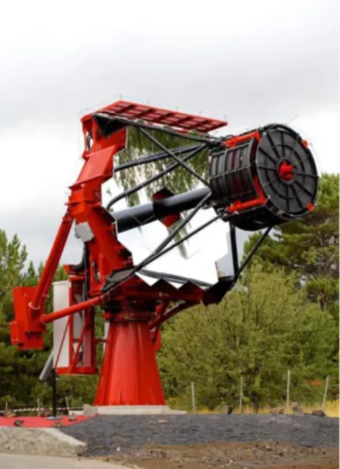
National Institute for Astrophysics (INAF). A set of (at least) nine ASTRI telescopes is foreseen to be installed during the initial implementation of the CTA southern site [9]. First purpose of the ASTRI Project has then been the construction of the ASTRI telescope prototype, according to the CTA scientific requirements. The prototype, named ASTRI SST-2M and shown in Fig.1, is installed at the “M.G. Fracastoro” INAF observing station in Serra La Nave on the Etna Mountain near Catania, Sicily, Italy. The prototype has been developed following an end-to-end approach [10] that includes development, deployment, operation and control of structure and mirrors [11], of camera and inner calibration system [12], software and hardware for control and acquisition [13,14], data reduction and analysis software [15], data archiving system [16] and the external equipment for monitoring and calibration purposes [17]. The telescope consists of a supporting structure including alt-azimuthal system, mirrors and camera. Controls, motion and sequences of complex telescope operations are performed by the Telescope Control System software package running on a dedicated workstation installed in the control room. The optical design of the ASTRI SST-2M telescope is based on a double mirror Schwarzschild-Couder [18] configuration consisting of two aspheric mirrors (4.3 m and 1.8 m diameter each) configured to correct spherical and coma aberrations keeping an angular resolution of at least 11.4 arcmin (0.19°) on a large field of view (~10 °) [19,20]. The telescope equivalent focal length is 2.15 m, f/0.5. The focal plane camera [21], designed to catch and record, during the night, the fast Cherenkov light pulses in the wavelength interval of 300-700 nm, consists of an array of monolithic multi-pixel Silicon Photo-Multiplier (SiPM) sensors coupled with a specifically designed front-end electronics [22]. The main features and performance of the ASTRI SST-2M camera will be described in the following sections. Technical details can be found in the citations along the text and references therein.
Figure 1: The ASTRI SST-2M telescope at Serra La Nave INAF observing station. (Image credit: Akira Okumura)
2. THE ASTRI CAMERA
The dual-mirror design that characterizes the optical system of the ASTRI telescopes results, among various things, in a small plate scale (37.5 mm/deg) leading to a camera of compact dimensions, allowing the use SiPM sensors assembled onto a curved focal plane located between the two mirrors. In the ASTRI camera the SiPM sensors are organized in 37 multi-pixel Photon Detection Modules (PDMs)1, each pixel with a sky-projected angular size of 0.19°, matching the
angular resolution of the optical system. This configuration yields a point spread function, which is characterized by a 80% containment diameter (D80) for a point-like source, contained in less than one camera pixel [20].
1 For the time being, the prototype camera consists of 21 out of 37 PDMs.
Proc. of SPIE Vol. 10702 1070237-2
Downloaded From: https://www.spiedigitallibrary.org/conference-proceedings-of-spie on 07 Oct 2020 Terms of Use: https://www.spiedigitallibrary.org/terms-of-use
Lids + motors
Fitter Window
M1
SiPM B FEE Focal plane
n
Thermal Control SystemAncillaries carrier BackEnd Electronics
Voltage Distribution board
BackBone Structure
The ASTRI focal plane is covered by a filter window and the entire camera [21], with its thermal control, electronics and all ancillary devices, is closed in a basket whose top is open thanks to a lid system. A novel inner fiber-optic equipment for relative calibration and a GPS receiver used for time synchronization and providing tag-time for triggered events, are part of the camera ancillary devices. The SiPM sensors exhibit very fast response and excellent single photoelectron resolution and they need properly tailored electronics devoted to directly interface the SiPM sensors, detecting the fast pulses produced by the Cherenkov flashes, managing the trigger generation, the digital conversion of the signals and the transmission of the data to the camera server external to the telescope. The ASTRI camera electronics [22] represents an innovative solution, being based on a custom peak-detector operation mode to acquire the SiPM pulses rather than the sampling technique adopted by other CTA telescopes. The SiPM read-out chip, with its signal shaper and peak detector customized for ASTRI, provides high efficiency auto-trigger capability and very fast camera pixel read out. The ASTRI camera trigger is a topological one, activated when a given number of contiguous pixels within a PDM presents a signal above a given photo-electron threshold. Data registered by the ASTRI camera at the occurrence of a trigger condition (scientific event) or when required (calibration or housekeeping data) are then sent to the camera server in which the camera data acquisition software is installed. A stable and precise (10 ns resolution) GPS (Global Positioning System) receiver provides events timestamp.
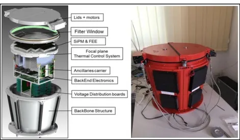
The truncated cone-shaped camera body dimensions for the ASTRI SST-2M prototype are 520 mm, 660 mm, 560 mm respectively (bottom diameter, height, top diameter) for a total mass of 73 kg. An exploded 3D view of the camera is shown in Fig. 2 together with the actual camera. A description of the camera subsystems is given in the following sections.
Figure 2: Explosed view of the ASTRI camera and the actual camera. 2.1 Lids
Two light-tight lids prevent accidental sunlight exposure of the focal surface detectors in case of direct light reflected by the mirrors and simultaneously allow to perform detector relative calibration even during day light. Opening and closing of the telescope lids are performed by means of two motor controllers SMCI12 by Nanotec [23] mounted in the motor box and located outside the camera. The stepper motor controller SMCI12 is an extremely compact and cost-effective constant current power output stage with integrated closed-loop current control. The RS485 controller is connected to the back-end board and managed by the on-board OPC-UA server [24].
2.2 Filter entrance window and fiber optical calibration system
To attenuate as much as possible the contribution coming from night sky background in comparison to Cherenkov emission, an infrared (IR) filtering window on the optical path has been implemented. The IR filter has been designed to cut the signal at wavelengths above 550 nm and is placed in front of the SiPMs, working both as filter and as protective window for the sensors. The IR filter was implemented as a series of three double coated substrates. This solution enables to reach high contrast, limiting the number of deposited layers. The substrates have been realized as circular synthetic fused silica (Spectrosil) plates with a diameter of 400 mm and thickness of 1.5 mm. Each coating is realized as ZrO2-MgF2 multilayer. With this solution a drop off of about 70% is achieved at wavelengths greater than 700 nm, as shown in Fig.3.
Proc. of SPIE Vol. 10702 1070237-3
Downloaded From: https://www.spiedigitallibrary.org/conference-proceedings-of-spie on 07 Oct 2020 Terms of Use: https://www.spiedigitallibrary.org/terms-of-use
100 90 80 70 ae 60 50 CN W H 40 30 20 10 Stadt 3 filters Single fittet
- - Stack Simylatior, (Single filter ^3)
200 250 300 350 400 450 500 550 600 650 700 750 800 850 900 950 1000 Waveinght (nm) 0.55 0.50 0.45 0.40 Á0.35 i, 0.30 g0.25 0.20 0.15 0.10 0.05
Signal /Noise Improving factor = t.89
0'0200 250 300 350 400 450 500 550 600 650 700 750 800 850 900 950 1000
Wavelrght [nm]
A 2-mm diameter optical fiber, illuminated by a blue laser diode, is placed in contact with the edge of the filter window. The laser diode emitted light can be continuous or pulsed (from two ns up). The light emitted from the optical fiber propagates inside the filter window where it is diffused/scattered uniformly illuminating the focal plane detector.
Figure 3: Spectrosil transmittance vs wavelength at photon incidence angles between 0° and 60° (left panel). The transmittance (averaged with respect to the incidence angle) of the filter window used in the ASTRI camera prototype (black curve) is superimposed to the Cherenkov and NSB spectrum (right panel) showing the drop off at wavelengths greater than 700 nm. 2.3 Photon Detection Module
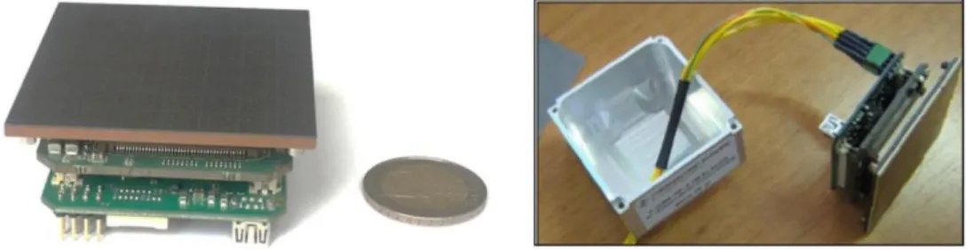
The Photon Detection Module (PDM) is the mechanical unit containing SiPMs board, FEE (Front End Electronics) and ARTIX 7 Xilinx FPGA (Field Programmable Gate Array) Printed Circuit Boards (PCBs). Each PDM module is mechanically interfaced to the PDM support structure through three bolts screwed from the bottom side of it. The PDMs support structure is composed of a spherical shape mounting interfaced to the electronics basket and to the backbone structure. The PDM support structure is machined out of standard flat plates of Al SiMgMn (EN AW-6082). An efficient thermal management is obtained embedding heat pipes into the PDM support structure. For the best thermal contact, heat pipes are bent and soldered into the metallic support. The PDM supporting structure hosts all the 37 PDM modules. PCBs are placed inside an aluminum box and fixed to it by means of four screws as shown in Fig.4.The PCBs are tightly packed together in order to minimize space and optimize the heat exchange among them.
Figure 4: PDM front-end electronics consisting of SiPM tile, ASIC and FPGA boards. The PCBs are accommodated in an aluminum case by means of four through screws.
The acquisition and the processing of SiPM pulses is performed by the electronics hosted in the PDM complying with pre-defined and invariant specification. The most demanding part of the PDM electronics is the analog FEE that must process the information contained in the signal pulses for further measurements as energy and pixel time tagging. The FEE is constituted by two (32 channels each) CITIROC [25] (Cherenkov Imaging Telescope Integrated Read Out Chip) ASIC (Application-Specific Integrated Circuit) interfaced to an ARTIX 7 FPGA whose functions are setup the CITIROC registers, read-out and deliver the digitalized data, manage the trigger signals and perform topological trigger algorithms.
2.4 Back-End electronics
The BEE is made up of a single board based on a powerful ZYNQ-7000 system-on-chip (SoC) FPGA device that manages the communication to/from the FEE and the external world. The BEE is in charge of the complete data and command management of the instrument, interfacing the detectors to the external world. It lies between the PDM front-end electronics and the Camera Server and Camera Controller System. It is the primary component of the real-time scientific data processing capability of the ASTRI SST-2M camera. It performs basic data assembly, formatting and processing
Proc. of SPIE Vol. 10702 1070237-4
Downloaded From: https://www.spiedigitallibrary.org/conference-proceedings-of-spie on 07 Oct 2020 Terms of Use: https://www.spiedigitallibrary.org/terms-of-use
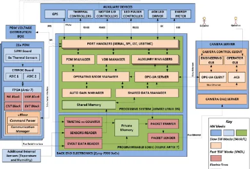
AUXMARY DEVICES THERMAL CONTROLLERS M PDM VOLTAGE DISTRIBUTION BOX 2L SiP } PENN Bevd al Sent CITIROC Board ASIC 1 ASIC2 I FPGA (Artis l)
MK Week VAR Neck
CM' Week EVFBIeek Ogler. Command Paner Communieatian Monoger Additional Internal Sensors (Teperature Humidity) and Humidity) MOTOR UD CONTROLLERS LED PULSER CONTROLLER ICH LED DRIVER ENERGY METER } } V E E
A. PORT HANDLERS (SERIAL, SPI, I2C, USBTMC)
II
H
I I
PDM MANAGER ADO MANAGER AUXILIARY MANAGERS
A
OPERATING MODE MANAGER +- OPC,UA SERVER
AUTO GAIN MANAGER SHARED DATA MANAGER
Shared Memory
A PROCESSING SYSTEM (ARMED UNDO OS)
-ss
TIMETAG ne COUNTER _ii.
-
MemoryPrivatePACKET FRAMER
SENSORS READER
PACKET SENDER
--EXERT DATA READER
PROGEAMMABLE LOGIC ()MINX ARTIX 7) BACK END ELECTRONICS (2yrp -7000 Sacs)
CAMERA SERVER
CAMERA CONTROL CLIENT ENGINEERING
GUI
OPERATOR GUI
OPOUA CLIENT
CAMERA DAQ SERVER
} Key 1/W blocks I II I I SlewSWbleakr (/AVA/C) I
Feat 'SW' blocke (VNOL)
I f
Elemia linea
services, and supports the desired procedure for real-time inspection of the camera data stream as well as other related processing activities. It is designed and implemented as a real-time data processing system capable of consuming and processing data and operations at a rate greater than or equal to the rate generated by the trigger of the telescope (up to 600 Hz). The BEE is connected via Ethernet to the camera control system GUI that provides all external commands and controls. The camera control system receives all errors, warning, performance and other reports from the BEE.
2.5 Power supply assembly
A voltage distribution board (VDB) constituted by a main board and 37 daughter boards provides the required regulated power to all the electronics devices of the camera. The VDB converts one low-voltage supply (24 V) input to individually protected outputs voltages. The VDB consists of power conditioning electronics based on DC/DC converters. Housekeeping functions as voltage or current quantities are available for monitoring of the VDB status. The units implement an overload and overvoltage protection circuitries in order to avoid failure propagation. Moreover, being each of the regulated power to SiPM programmable by user, they absolve automatically to the SiPM gain compensation adjusting the voltage at varying of temperature.
2.6 Thermal system assembly
A grid of heat pipes, inserted on the reverse side of the PDM support structure, are part of the thermal system assembly to minimize the temperature gradient between each of the PDM modules. Thermoelectric coolers (TECs) are used to remove heat from the PDMs, and maintain a constant temperature at the surface of the PDM itself. The heat generated from the TEC devices is then transferred into heat pipes below the focal plane, where it is transported to fin stacks and removed by forced-convection with air supplied via fans. The thermal system performs the required operations to assure a proper working temperature to the camera electronics (from +15 °C ± 2 C°) and in particular to maintain SiPMs at a constant temperature. Thermoelectric system makes use of a Bi-Directional Thermostatic Controller that can operate in both heating and cooling mode providing temperature control and system functions, including separate fan control, low voltage protection, and alarm. The RS232 interface allows reading and controlling parameters as well as real-time functions setting.
2.7 Camera software architecture
All the devices and systems are interconnected to the BEE, which is the main elaboration unit of the camera, managing all its functions. The camera software is in charge of receiving commands from the camera control client, controlling and monitoring the auxiliary devices, managing and acquiring data from the PDMs, preparing and sending packets to the camera data acquisition server where Data Acquisition (DAQ) software performs real time analysis and data archiving [26]. A schematic of the camera software architecture is shown in Fig.5.
Figure 5: Schematic of the software architecture of the camera.
Proc. of SPIE Vol. 10702 1070237-5
Downloaded From: https://www.spiedigitallibrary.org/conference-proceedings-of-spie on 07 Oct 2020 Terms of Use: https://www.spiedigitallibrary.org/terms-of-use
eI 0 Charge measurement
--q-
read'
low gain 8 -bit input DAC Preamp I PD (' Low gain--t
multiplexed output I Ixi
ENV`Preamp high gain PD
High gain multiplexed output
1--II
Trigger read -+rsh y -bit DAC !J Mask RS Trigger multiplexed output x32 1, t {a -b't one OP'.bandag p Temperaturesensor Dual DAC
Common to the 32 channels
l0 -bit DAC 1 lobtone
-LG Low_gain multiplexed output HG High_gain multiplexed output Charge trigger TRIGGER Time_trigger OR32_charge OR32_charge_OC OR32_time_OC3. FIRST RESULTS AND PERFORMANCE
All components of the ASTRI camera as well as the fully-assembled camera have been tested in lab and on field. Procedures for relative SiPM gain calibration, trigger alignment, clock synchronization and data transmission have been implemented and tested carefully. The goal of lab tests and on site camera tests is to verify and possibly improve the system reliability and stability.
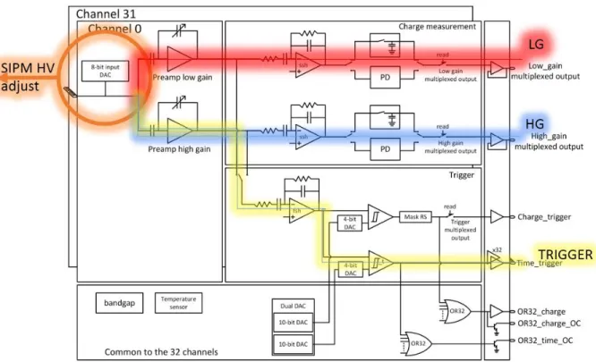
A schematic view of the typical signal processing path of each CITIROC channel is shown in Fig. 6. This oversimplified scheme actually describes the whole signal processing chain and is valid for each channel (pixel) of the camera.
Figure 6: General block scheme of the CITIROC ASIC. Colored paths identify the LG, HG and TRIGGER chains.
Each CITIROC is characterized by separate chains for high gain (HG), low gain (LG) and trigger outputs. Each CITIROC channel implements an 8-bit DAC for SiPM gain adjustment. The pulse generated by the SiPM is processed by the AC-coupled CITIROC electronic channel. It is amplified by means of two programmable preamplifiers (nominal Gain=3.3 for LG and nominal Gain=66.6 for HG) and then shaped (nominal shaping time = 25 ns) with two shaper circuits (LG and HG) respectively. The gain values have been chosen to obtain a dynamic range from 0 to about 60 photoelectrons for the HG channel and from 0 to about 1300 photoelectrons for the LG channel. A bipolar fast shaper (FSH in Fig.6) connected to the high gain preamplifier produces a fast signal (~15 ns shaping time) that is connected to a discriminator with a 10 bits-DAC programmable threshold. The output of the discriminator gives a digital signal (trigger) if the input signal exceeds the threshold level. The peak detector or single channel analyzer (track&hold mode) are selectable via slow-control configuration bits. The base-line operational mode is peak detector. Peak detector captures the most positive point of the input signal so that the maximum of the shapers signals represents the pulse height conversion of the SiPM output signal. The digital triggers (64 channels for each PDM) are available on the 32 + 32 output pads of the two ASICs constituting the unit module based on 64 pixels. The analog outputs of the peak detectors are stored into 64 analog memories and read, at the occurrence of a trigger condition, by multiplexing the three-state output registers (LG and HG respectively) and then converted to digital counts by external ADC devices. The Artix 7 FPGA manages all the input/output operations from/to CITIROCs and SiPMs.
Proc. of SPIE Vol. 10702 1070237-6
Downloaded From: https://www.spiedigitallibrary.org/conference-proceedings-of-spie on 07 Oct 2020 Terms of Use: https://www.spiedigitallibrary.org/terms-of-use
3.1 In lab
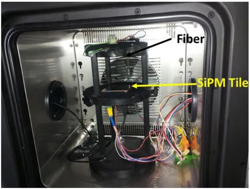
The calibration procedures developed and implemented in lab are the necessary starting points to perform the "on field" camera calibrations without the aid of lab instrumentation. The laboratory measurements have been done using the setup shown in Fig.7, consisting of a climatic chamber where a transparent acrylic disk surrounded by an optical fiber pulsed by a LED, irradiates light almost uniformly on the SiPM tile. The climatic chamber assures a constant temperature on the SiPM tile under test with a precision of ~0.3°C and stability of ~0.1°C. The expected average and gradient temperature inside the camera as well as the differences in Vop (SiPM operating voltage) between pixels and the desired minimization
of pixel optical cross-talk leads to define a reference SiPM operating voltage for a reference temperature.
Figure 7: Lab. set-up used for the relative gain calibration of the electronics chain (front-end) and SiPM sensors.
3.1.1 Relative gain calibration
The relative gain calibration aims to uniform the response function of each channel (pixel) including the small differences between SiPM pixel gain and front-end channels. The causes of non-uniformity are numerous although usually small differences in SiPM gain and voltage reference of the front-end discriminators are the main issue.
The manufacturer, Hamamatsu Photonics, provided the reference values of the operating voltage Vop (at 3 V of
overvoltage) and the gain at temperature of 25°C for each physical pixel (7mm x 7 mm) of the S10943-4286(X) SiPM tile. Characterization and estimation of the main features of SiPM detectors [27] has been carried out using integrating sphere, calibrated photodiode and ASTRI electronics at the COLD (Catania Observatory Laboratory for Detector) lab, a research facilities of the INAF – Osservatorio Astrofisico di Catania.
The SiPM gain, operating in Geiger-mode, grows linearly with the operating voltage according to:
q
V
V
C
q
Q
G
tot
pixel(
op
bd)
(1)where Qtot is the total charge generated by a discharge (avalanche), Cpixel is the overall pixel capacitance, q is the electron
charge, Vop is the operating voltage and Vbd is the SiPM breakdown voltage.
Proc. of SPIE Vol. 10702 1070237-7
Downloaded From: https://www.spiedigitallibrary.org/conference-proceedings-of-spie on 07 Oct 2020 Terms of Use: https://www.spiedigitallibrary.org/terms-of-use
250
-200150
-
10050
-
0-Mali
.
'pe
2'pe 3' pe Pe 5'pe 6'pe 7"pe 8' pe9'p
eHGpix
1 2200 2300 ADC 1 1 A"t1--*
2400The SiPM gain is a function of the differences between the two voltages Vbd and Vop. The breakdown voltage is a
characteristic of the SiPM physical pixel and is mainly sensitive to temperature, while the operating voltage is different for each pixel within few hundreds of mV. The operating voltage can be opportunely tuned to keep the pixels gain uniform and stable in time against temperature variations in Vbd.
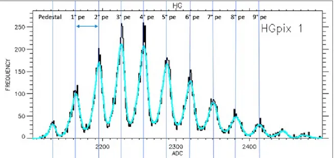
The gain calibration procedure has been implemented for each PDM (8×8 pixels) pulsating a blue LED at a constant rate of 10 kHz and a pulse time-on duration of 5 ns maintaining at 15°C the temperature of the climatic chamber. The temperature of the SiPM pixels is taken by means of nine calibrated temperature sensors symmetrically spaced on the rear side of each SiPM board. Measurements of the pulse height for a sample of 10000 events triggered by LED pulses are then acquired with pixels temperature stabilized at 15°C ± 0.3°C. The histogram of the pulse height distribution is shown in Fig.8 for one channel (pixel).
Figure 8: Pulse height distribution demonstrating the SiPM capability to resolve single photoelectron. The distance between consecutive peaks measures the pixel gain in ADC counts.
The gain of each SiPM pixel is calculated from each histogram of data gathered from the pixel and smoothed with a boxcar averaging of specific width starting from the second peak representing the first photoelectron (pe). Photoelectron equivalent gain (peeq) pixel by pixel has been obtained by determining the arithmetic mean of the distances between
successive local maxima applying equation (2):
)
(
1
)
(
1 1 i N i i eqADC
ADC
N
ADC
pe
(2)It represents the gain of the HG channel in ADC counts per peeq; ADCi is the ADC value of the local maximum of the i-th
peak on the histograms while N is the number of peak intervals. Pixel gains and pedestals as obtained through the calibration are used in the off-line analysis. The calibration provides the required conversion coefficients from ADC counts to photoelectrons. The calculation of the amplitude in photoelectrons received by each pixel is:
eq pe m
pe
ADC
ADC
Npe
1
1 (3) where Npe is the number of pe, ADCm is the measured ADC counts, ADC1°pe is the ADC count of the first pe and peeq thegain of the HG channel in ADC counts per pe.
Fig. 9 underlines the strength of this method when the conversion equation (3) is applied to a data set without calibration (using nominal values for Vop and gain) and a data set with end-to-end calibration.
Proc. of SPIE Vol. 10702 1070237-8
Downloaded From: https://www.spiedigitallibrary.org/conference-proceedings-of-spie on 07 Oct 2020 Terms of Use: https://www.spiedigitallibrary.org/terms-of-use
..>" n.., rwa w.-ob.s. . p :1 .#`F
a # 4 4 4
Iryy. u... 1, .ayw:l F 1,i
p.il T
aiP: J. -. . . . . , _ .. , . ..w , .w 4/ /.+ . . rr .!J rr r
rw l' ..w f.* a i s a r a a al
al
irT ;.r"
r--f`'
4 ... r..
it
a
60 50 40 m '-'2-- 30 CJ
20 10 o 0 10 20 30 40 HG (pe) 50 60 1200 1000 800 C = o 600 U 400 200 1, 71--ti . -2 0 2 4 6 HG-LG (pe)Finally, LG calibration is performed using the HG calibration parameters and the LG pedestals. Fig. 10 shows the scatter plot of LG pe as a function of HG pe for a pixel. The plot exhibits a linear correlation between converted LG and HG pe number.
Figure 9: The left panel shows 16 pixels not calibrated while the right panel shows the same pixels calibrated. It is easy to see the misssing pe alignment for not calibrated pixels while good alignment is obtained for calibrated pixels. Moreover, it is evident how much the dispersion around the average pe value is strongly improved for calibrated pixels.
Figure 10: Scatter plot of LG as a function of HG which shows linearity and average dispersion of about 1.5 pe.
=1.46 pe
Proc. of SPIE Vol. 10702 1070237-9
Downloaded From: https://www.spiedigitallibrary.org/conference-proceedings-of-spie on 07 Oct 2020 Terms of Use: https://www.spiedigitallibrary.org/terms-of-use
260 280 300 32( 40 360
OnC count 380
Count 360 380
3.1.2 Trigger signals equalization
Digital trigger signals are generated when the analog input signals exceed a set threshold level in the discriminators. The ideal situation would be to have an equal response from all trigger channels for a given trigger threshold. Actually, small differences between channels due to the ASIC processing technology produce a non-uniform response at the nominal threshold. CITIROC, however, is capable to compensate this trigger non-uniformity using, for each channel, a 4-bits DAC with the aim to finely adjust and hence equalize the trigger response at the given threshold level. It is worth to remember that any of at least 4 adjacent pixels, set to an equal threshold and for any PDMs, generates the first trigger level of the camera. This specific trigger configuration mitigates, to some extent, the requirement for fine triggers equalization. However, since less stringent trigger setting could be used for other calibration needs, trigger signals equalization is simply performed. It must be said that the 4-bit DAC needs to be set only once for all channels, thanks to the stability of CITIROC with the temperature.
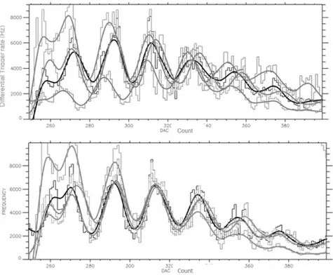
Trigger signals equalization is determined performing the “Staircase” functions or rate curve measurement after doing gain equalization. Staircase is the integral distribution of the pixel pulses rate with increasing discriminator threshold at a given applied voltage. Fig. 11 plots the derivative of the staircase curves showing the differences in offset of four CITIROC channels. The maximum difference between channels of the same ASIC is about 6 DACs.
Figure 11: Trigger measured offset of four CITIROC channels without offset adjustment (up panel) and with offset adjustment (down panel) (see text).
3.1.3 Current monitoring by Variance
This technique is based on the statistical analysis of the variability of the signal detected by the camera front-end electronics. It considers the randomly-repeated sampling of the electric signal generated by each pixel not triggered by the first level trigger. The net result is, for each pixel, a sequence of ADC values whose average is constant with time, but whose variance is proportional to the flux impinging on the pixel. The variance technique, working in parallel with the standard detection Cherenkov pipeline, allows us to indirectly measure the sky background flux and therefore to investigate variations in the atmospheric attenuation and to monitor the presence of clouds and stars in the telescope field of view. Moreover, since the positions of the stars are known with a high accuracy, the effective pointing of the telescope
Proc. of SPIE Vol. 10702 1070237-10
Downloaded From: https://www.spiedigitallibrary.org/conference-proceedings-of-spie on 07 Oct 2020 Terms of Use: https://www.spiedigitallibrary.org/terms-of-use
can be determined by measuring the shift between the actual positions of the stars and the nominal ones in the images generated by the variance method. Furthermore, these images may reveal possible misalignments among mirrors.
3.2 On field
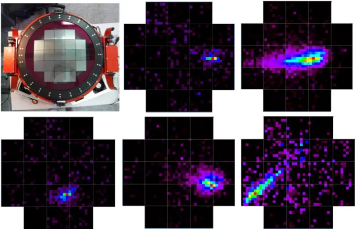
After initial commissioning in the lab, the integration of the ASTRI prototype camera with the telescope was carried out in May 2017. Although the runs were mainly engineering with only a few PDMs active, the first Cherenkov events were observed, allowing us to achieve the "first light" [28]. In the following months and when possible due to the weather conditions, more intensive engineering tests have been carried out until today. All the 21 PDMs that currently form the focal plane of the camera prototype are now fully working. Fig.12 shows the camera prototype and a few selected Cherenkov events out of thousands taken during the first scientific runs.
Figure 12: The picture on the upper left corner of the figure shows the camera with opened lids. The 21 PDMs at the focal plane of the prototype camera can be easily recognized. The remaining figures shows the images of detected Cherenkov events during on-sky observations.
3.2.1 Camera performance
During the on-site commissioning, housekeeping (HK) monitoring has been activated. The HK information is relevant to check the correctness concerning camera cooling system, voltage distribution, temperatures inside the camera and of the SiPM tiles. Furthermore, a successful test has been performed on the real-time compensation of the SiPM Vop as a function
of temperature variations. Feedback from the temperature sensors of each PDM allows to regulate the SiPM operating voltage within ±0.33°C, corresponding to a change in Vop of about ±18 mV. Fig. 13 shows the 21-temperature profiles of
the nine/PDM temperature sensors. The profiles are related to a continuous operation starting with the camera in OFF state, it is switched-on as soon as the temperature reaches the reference value settled in the thermal control; this phase requires about 110 minutes. Fig 14 shows the compensation of the SiPM voltage when the temperature changes. As expected, the trend of Vop compensation profile follows the trend of the temperature measured on the SiPM from which a constant gain
level is achieved.
Proc. of SPIE Vol. 10702 1070237-11
Downloaded From: https://www.spiedigitallibrary.org/conference-proceedings-of-spie on 07 Oct 2020 Terms of Use: https://www.spiedigitallibrary.org/terms-of-use
r
s
a asel
w2ws
lletlw
i
I
ii
i
1If
i
I les,e w ..ti 11121111 w wI
22202 teta: e ..0e....
I IIf
II
1 1 I iIt
3Iia
i
1 II;
Ij
I eela w triaep
w wI
1 II 1I
I
ii
of aI
. 22202 e:..eKe, Die"
1
efiM w wS
ten* ea w1
I
I
1tII
I
I
II
If
i
It
II IIt
II f 1 1II
I III
I It
II
ItII
I.
...
..
. Mt NO lese, Ns /e bi say w.wI
I
i
II
II
I
I
0.01, bi lab w45" tine w.n. .2r++a.....
1i
sesse 4AUGHTER 5 = 56.9957 V v= 0.0474 y 10--0 I I 1 . . . . , , . . r I 1 1000 2000 3000 4000 5000Time bin (1 sec.)
I ®000
m
3
AIr,
tirFigure 13: Temperature sensors profiles of all the 21 PDMs.
Figure 14: Temperature time profile of the central temperature sensor and resulting SiPM Vop adjustment. It should be noted that the Vop adjustment steps follow the trend of the temperature profile.
Proc. of SPIE Vol. 10702 1070237-12
Downloaded From: https://www.spiedigitallibrary.org/conference-proceedings-of-spie on 07 Oct 2020 Terms of Use: https://www.spiedigitallibrary.org/terms-of-use
Very preliminary telescope trigger rates as a function of pixel trigger thresholds for a topological trigger of at least five-pixel contiguous five-pixel coincidence has been carried out. The five-five-pixel coincidence rate is shown in Fig. 15. It displays three separated features. For thresholds less than six pe it is evident the saturation due to the finite-resolution of the counting electronics. From six pe up to 10 pe the coincidence rates fall steeply with increasing thresholds being dominated by NSB random coincidences. Above ten pe is evident the region where the measured rates are dominated by ordinary air showers events. Fitting the trigger rates data as a function of threshold with a power law spectrum gives a spectral index of -1.25 ± 0.04. The resulting power-law slope of the rate curve is a little smaller (about 30% less) than the cosmic-ray integral spectral index. This may be due to several reasons, as for example, influence of fluctuations, mirror miss-alignment and mirrors reflectivity degradation, slightly flat field differences between PDM causing increases of the telescope energy threshold. All these potential causes will be investigate in details and will be the subject of the forthcoming measurements.
topological trigger 5 pixel contiguous
Pixels trigger threshold (pe)
4 6 8 10 12 14 16 18 20 22 24
tele
s
c
o
p
e
tr
igg
e
r r
a
te (
Hz)
100 101 102 103 104 105 106
Figure 15: Five-pixel coincidence integral trigger rate as a function of the trigger threshold in photoelectrons. Also shown are the trigger rate saturation (green line) and the random coincidence rates (black dashed line) induced by the NSB diffuse light. The red dashed line represents a power-law fit to the data points for thresholds greater than 10 pe. The telescopes were pointed at a dark region of the sky near the zenith.
3.2.2 Variance at work
Variance test runs, somewhat new for Cherenkov telescopes, have been also performed with closed lids and open lids during the few nights with clear sky. Variance of the focal plane pixels is shown in Fig. 16. It is obtained with closed lids and SiPM operating in dark current. The use of the Variance technique turns out to be effective in quickly check the pixels health. As shown in the figure, pixels with different level of noise and dead pixels can easily be identified. For example, noise pixels with less than 0.4 pe have been recognized as the perturbed ones by their proximity to the switch mode dc-dc converter located in the FPGA PCB board.
Proc. of SPIE Vol. 10702 1070237-13
Downloaded From: https://www.spiedigitallibrary.org/conference-proceedings-of-spie on 07 Oct 2020 Terms of Use: https://www.spiedigitallibrary.org/terms-of-use
Figure 16: Focal plane pixels Variance. Only few seconds of variance runs allow extracting the above information. This procedure is intended to be used routinely every night before and after open-sky scientific observation.
A further application of the variance technique, among others, consists in pointing one or more bright stars as shown in Fig. 17. Pointing the telescope to the Orion belt, the image of three more brilliant stars appears. Around the three stars it can be recognized spot points that after a more accurate analysis reveal to be “ghosts” caused by misalignment of four of the primary mirror panels.
Figure 17: On the left the image of the Orion belt as produced by the variance technique. On the right Stellarium screen image showing the same sky region. The intense signal from the stars allows to estimate the PSF of the optics that results in line with the measured one with CCD optical camera.
3.3 Lessons learnt
Open-sky operation has proven to be essential in understanding system stability and reliability. During the first period of the on-site commissioning several issues have been found and resolved. Among them, cabling problems, firmware tuning both on FEE and BEE have been the main concerns. At present, a major concern is represented by irregular missing signals from the HG channels when the camera operates with open lids. This behavior has been found analyzing the data set of the scientific observations where unexpected “holes” in the Cherenkov images are evident. The problem, that does not affect in any way the LG channels, is currently under deep investigation through very exhaustive and systematic tests in lab.
Proc. of SPIE Vol. 10702 1070237-14
Downloaded From: https://www.spiedigitallibrary.org/conference-proceedings-of-spie on 07 Oct 2020 Terms of Use: https://www.spiedigitallibrary.org/terms-of-use
4. TOWARDS THE MINI-ARRAY
The ASTRI mini-array telescopes are conceived as the pre-production of a limited set (9) of telescopes for the CTA for which it is necessary to undertake the process of industrialization that will lead to their production. In the product development process, one of the key steps is creating a sample of the product before it is manufactured. The ASTRI SST-2M prototype is an initial creation of a product that shows the basics of what the product will look like, what the product will do, and how the product operates. As well as the telescope structure also the prototype camera is not meant to be the final version; it is the preliminary form of the product. The ASTRI prototype camera has elements that demonstrate how the camera will work and the full functionality is only expected after it will be industrially manufactured. The prototype helps to get and define the level of quality and readiness required for industrial engineering. The ASTRI mini-array camera will take into account the very useful information obtained from the camera prototype solving all the weak points that have emerged. It will also improve the detection performance by introducing the newest SiPM sensors regularly manufactured according to the continuous and inexorable progress on the silicon light sensor technology. In fact, the latest SiPMs generation shows an increased Photo Detection Efficiency (PDE) of almost a factor 2, a reduced optical cross talk and an enhanced detection efficiency to the ultraviolet wavelengths, as compared to the ones used in the prototype camera. All of that translates into a lowering of the energy threshold for Cherenkov detection. Another envisaged improvement consists in optimizing the firmware of the FPGA front-end in order to allow signal processing with shaping time of 12.5 ns as compared to the actual one of 25 ns. Signal processing with shaping time of 12.5 ns translates also into a lowering of the energy threshold due the expected increasing of the signal to noise ratio. Finally yet importantly, to avoid camera malfunctioning, all cabling and mechanical parts of the camera will be carefully cured.
5. CONCLUSIONS
Calibration procedures have been developed and implemented for the ASTRI prototype camera. The calibration algorithms and the calibration coefficients have been extensively tested in lab and on field showing a good agreement. Looking at the preliminary results on field, the camera calibration method seems to be robust and accurate. Variance technique gives a significant benefit in improving system performance. More work is certainly needed to complete all the necessary tests before starting with the science verification phase. Moreover, the behavior of the HG channels has to be understood correctly and resolved in order to achieve the full performance of the camera. The huge work done on the prototype camera and on telescope too is for sure of paramount importance in view of the ASTRI mini-array implementation.
ACKNOWLEDGMENTS
This work was conducted in the context of the CTA ASTRI Project. This work is supported by the Italian Ministry of Education, University, and Research (MIUR) with funds specifically assigned to the Italian National Institute of Astrophysics (INAF) for the Cherenkov Telescope Array (CTA), and by the Italian Ministry of Economic Development (MISE) within the “Astronomia Industriale” program. We acknowledge support from the Brazilian Funding Agency FAPESP (Grant 2013/10559-5) and from the South African Department of Science and Technology through Funding Agreement 0227/2014 for the South African Gamma-Ray Astronomy Programme. We gratefully acknowledge financial support from the agencies and organizations listed here: http://www.cta-observatory.org/consortium_acknowledgments. This paper has gone through internal review by the CTA Consortium.
REFERENCES
[1] Acharya, B.S. et al., The CTA Consortium, “Introducing the CTA concept”, Astroparticle Physics 43 (2013) 3-18 [doi: 10.1016/j.astropartphys.2013.01.007]
[2] The CTA Consortium, represented by R.A. Ong, “Cherenkov Telescope Array: the next generation gamma-ray observatory”, Proc. 35th ICRC (2017), PoS(ICRC2017)1071
[3] Montaruli, T., Pareschi, G., Greenshaw, T., for the CTA Consortium, “The small size telescope projects for the Cherenkov Telescope Array”, Proc. 34th ICRC 2015 (2016), PoS (ICRC2015)1043
[4] Heller, M., et al., “The single mirror small sized telescope for the Cherenkov telescope array”, AIP Conference Proceedings 1792, 080003 (2017)
[5] Le Blanc, O., et al., for the CTA GCT project, “Towards final characterisation and performance of the GCT prototype telescope structure for CTA”, Proc. 35th ICRC (2017), PoS(ICRC2017)836
Proc. of SPIE Vol. 10702 1070237-15
Downloaded From: https://www.spiedigitallibrary.org/conference-proceedings-of-spie on 07 Oct 2020 Terms of Use: https://www.spiedigitallibrary.org/terms-of-use
[6] R. White, R. and Schoorlemmer, H., for the CTA GCT project, “A Compact High Energy Camera (CHEC) for the Gamma-ray Cherenkov Telescope of the Cherenkov Telescope Array”, Proc. 35th ICRC (2017), PoS(ICRC2017)817
[7] Pareschi, G., et al., for the ASTRI Collaboration and the CTA Consortium, “The dual-mirror Small Size Telescopes for the Cherenkov Telescope Array”, Procs. 33rd ICRC, ArXiv:1307.4962 (2013).
[8] Pareschi, G., for the ASTRI Collaboration and the CTA Consortium, “The ASTRI SST-2M prototype and mini-array for the Cherenkov Telescope Array”, Proc. SPIE 9906, 99065T (2016) [doi: 10.1117/12.2232275]
[9] Scuderi S., for the CTA ASTRI Project, “From the Etna volcano to the Chilean Andes: ASTRI end-to-end telescopes for the Cherenkov Telescope Array”, these proceedings SPIE (2018)
[10] Maccarone, M.C., for the CTA ASTRI Project, “ASTRI for the Cherenkov Telescope Array”, Proc. 35th ICRC (2017), PoS(ICRC2017)855
[11] Antolini, E. et al., for the CTA ASTRI Project, “Telescope Control System of the ASTRI SST-2M prototype for the Cherenkov Telescope Array”, Proc. ICALEPS (2017) Paper THMPL04
[12] Sangiorgi, P. et al., for the ASTRI Collaboration and the CTA Consortium, “The software architecture of the camera for the ASTRI SST-2M prototype for the Cherenkov Telescope Array”, Proc. SPIE 9913, 99133T (2016) [doi: 10.1117/12.2231647]
[13] Conforti, V. et al., for the CTA ASTRI Project, “The DAQ system support to the AIV activities of the ASTRI camera proposed for the Cherenkov Telescope Array”, these proceedings SPIE (2018)
[14] Gianotti, F. et al., for the CTA ASTRI Project, “The ACS-OPC UA based ICT monitoring system of the ASTRI SST-2M prototype proposed for the Cherenkov Telescope Array” , these proceedings SPIE (2018)
[15] Lombardi, S. et al., for the CTA ASTRI Project, “ASTRI data reduction software in the framework of the Cherenkov Telescope Array”, these proceedings SPIE (2018)
[16] Carosi, A. et al., for the ASTRI Collaboration and the CTA Consortium, “ASTRI SST-2M archive system: a prototype for the Cherenkov Telescope Array”, Proc. SPIE 9910, 99101V (2016) [doi: 10.1117/12.2231646] [17] Segreto, A. et al., for the ASTRI Collaboration and the CTA Consortium, “The absolute calibration strategy of
the ASTRI SST-2M telescope proposed for the Cherenkov Telescope Array and its external ground-based illumination system”, Proc. SPIE 9906, 9906S (2016) [doi: 10.1117/12.2231922]
[18] Vassiliev V., Fegan, S., Brousseau, P., “Wide field aplanatic two-mirror telescopes for ground-based gamma-ray astronomy”, Aph, 28, 10 (2007)
[19] Canestrari, R. et al., for the ASTRI Collaboration and the CTA Consortium, “The ASTRI SST-2M prototype for the Cherenkov Telescope Array: opto-mechanical performance”, Proc. SPIE 9906, 990619 (2016) [doi: 10.1117/12.2232270]
[20] Giro, E. et al., “First optical validation of a Schwarzschild Couder telescope: the ASTRI SST-2M Cherenkov telescope”, Astronomy and Astrophysics (2017) October 11, 2017 [doi: https://doi.org/10.1051/0004-6361/201731602]
[21] Catalano, O., et al., for the ASTRI Collaboration and the CTA Consortium, “The camera of the ASTRI SST-2M prototype for the Cherenkov Telescope Array”, Proc. SPIE 9147, 91470D (2014); doi:10.1117/12.2055099 [22] Sottile, G. et al., for the ASTRI Collaboration and the CTA Consortium, “ASTRI SST-2M camera electronics”,
Proc. SPIE 9906, 99063D (2016) [doi: 10.1117/12.2232464] [23] Nanotec,SMCI12 Stepper Controller technical manual:
http://en.nanotec.com/fileadmin/files/Handbuecher/Motorcontrols/SMCI12_Technical- manual_V1.2.pdf [24] OPC Unified Architecture, Specification, Part 1: Overview and Concepts, Release 1.02, July 10, 2012":
https://opcfoundation.org/developer-tools/specifications-unified-architecture/part-1-overview-and-concepts [25] Fleury, J., et al., “Petiroc and Citiroc: front-end ASICs for SiPM read-out and ToF applications”, JINST 9
C01049 (2014)
[26] Conforti, V., et al., “The DAQ system support to the AIV activities of the ASTRI camera proposed for the Cherenkov telescope array”, these proceedings SPIE (2018)
[27] Romeo, G., et al., “Characterization of a 6×6-mm2 75-μ m cell MPPC suitable for the Cherenkov Telescope
Array Project”, Nuclear Instruments and Methods in Physics Research A, vol. 826, pp. 31-38, 2016. [28] CTA Press Release, 14 June 2017 (2017)
https://www.cta-observatory.org/cta-prototype-telescope-astri-achieves-first-light/
Proc. of SPIE Vol. 10702 1070237-16
Downloaded From: https://www.spiedigitallibrary.org/conference-proceedings-of-spie on 07 Oct 2020 Terms of Use: https://www.spiedigitallibrary.org/terms-of-use