1
Alma Mater Studiorum – Università di Bologna
DOTTORATO DI RICERCA IN
SCIENZE CHIMICHE - Ciclo XXV°
Settore Concorsuale di afferenza: 03/A2 – Modelli e Metodologie per le Scienze Chimiche Settore Scientifico disciplinare:CHIM/02 – Chimica Fisica
TITOLO TESI:
EXCITONIC PROCESSES IN MULTIFUNCTIONAL ORGANIC
SEMICONDUCTORS FOR APPLICATION IN ORGANIC
LIGHT-EMITTING TRANSISTOR
Presentata da: Stefano Troisi
Coordinatore Dottorato
Relatore:
Prof. Adriana Bigi
Prof. Giorgio Orlandi
Correlatore:
Dott. Michele Muccini
2
Contents
Introduction
….……….………...………..……4References………..……….…7
Chapter 1. Organic Semiconductors
1. 1 Introduciton Materials ………..………..………81.2 Optical properties in solid state ……..………..………..….10
1.2.1 Exciton in molecular crystal………..………….….11
1.2.2 Exciton generation, diffusion and relaxation………13
1.3 Eletrical properties ……….………...15
1.4 Overview on OLETs ………...………17
1.4.1 Working principle of OFETs………18
References………21
Chapter 2. Experimental Setup
2.1 Quantum Yield measurement………242.2 Steady-State Photoluminescence at low temperature………..……26
2.3 Ti: Sapphire Laser………..……28
2.4 Streak Camera……….……29
2.5 Confocal Laser Scanning Microscopy (CLSM)……….…………..30
2.6 Atomic Force Microscopy (AFM)………...33
2.7 Thin-Film growth by Vacuum Sublimation………...…36
3
References………..………..………39
Chapter 3. Synthesis and Optical properties in solution of T4DIM
3.1 Introduction……….……..413.2 Synthesis of T4DIM………..………43
3.3 Linear optical properties of T4DIM in solution 3.3.1 Absorption and Fluorescence Spectroscopy……..……….……….44
3.3.2 Time Resolved Spectroscopy..……….…….……….………...50
3.4 Theoretical Analysis……….………..53
References………..……….55.
Chapter 4. Optical Properties of T4DIM in ultra thin-films
4.1 Introduction: Role of molecular packing in determining solid-state optical properties of π-conjugated materials………..….574.2 X-ray analysis of T4DIM in single crystal and thin film………58
4.3 Thin-films of T4DIM on different substrates 4.3.1 Introduction………..61
4.3.2 Steady-state absorption and fluorescence………..62
4.3.3 PL at low temperature………65
4.3.4 AFM and CLSM investigation……….……….………67
4.4 T4DIM on PMMA substrate……….…..…………68
4.5 Optoelectronic performance of T4DIM in single layer transistor………..………74
References……….……...77
4
Introduction
In the past few decades, π-conjugated organic materials have attracted considerable attention in view of their increasing use as active elements in electronic and optoelectronic devices such as light-emitting diodes, photovoltaic cells, and field effect transistors[1,2]. Prototype systems of devices making use of organic materials are currently available, and the focus now is on improving device performances.The active semiconducting materials can be divided into two broad classes: π-conjugated molecular systems[3,4] which present precisely defined structures, and π-conjugated polymers[5], which are composed by repeating units and described by molecular weight distributions.
To achieve the maximum performance output from these devices, challenges arise from considerations that reach beyond the molecular chemical formula[6]. For isolated molecules, guidelines exist that rely on the molecular formula to tailor the frontier (HOMO-LUMO) molecular orbital energy levels and optical absorption profiles. Much less control can be achieved over relevant properties, that determine the features in the solid state. An important issue in organic electronic and photonics research is to understand the transition from simple conjugated building blocks to extended semiconducting molecules with predictable properties, and ultimately to the collective behavior of multiple components in functional devices[7].
In this direction, Organic Light-Emitting Transistors (OLETs) can be considered as a powerful platform for investigating the intimate correlation between solid-state molecular arrangement and functional properties in organics. OLETs are an innovative class of multifunctional devices in which the fundamental optical and electronic processes (such as charge transport, exciton formation, energy/charge transfer, charge trapping, etc.) are strictly connected to the active materials deposited as thin-film. It is well-known that in organic field-effect transistors, charge carrier mobility has a length scale dependence and only the first two molecular layers next to the dielectric interface contribute to the charge transport. Thus, device optoelectronic performance are mainly governed by the organic semiconductor aggregation and morphological features at the interface with the dielectric layer. As a consequence the molecular arrangement is extremely sensitive to the deposition procedures and to the nature of the substrate[8], thus it is possible to modulate the film morphologies playing with these parameters. Moreover, many studies have
5 shown how the degree of molecular order in organic thin film affects the optical[9]
and electrical[10] properties.
In this thesis, I report on a comprehensive study about the photo-physical properties both in solution and in solid-state of a new thiophene based material
(2,2’-(2,2’-bithiophene-5,5’-diyl)bis(5-butyl-5H-thieno[2,3-c]pyrrole-4,6)-dione (T4DIM) which shows an ambipolar semiconducting behavior together with electroluminescence in single-layer OLET device architecture[14]. This organic semiconductor is characterized by end substitution of a bithiophene core with two strong electron-withdrawing thieno(bis)imide moieties. Despite the numerous structures realized so far (i.e. of different sizes, substitutions, shapes, etc..)[11] materials combining both ambipolar charge transport and efficient electroluminescence are still a synthetic challenge, as these properties typically exclude one another in the solid state[12]. In this context, the substitution of oligothiophene materials[13-14] with strong electron-withdrawing moieties as for instance thieno(bis)imide units resulted as a powerful tool to obtain also electron transporting polythiophenes.
In this thesis I cross-correlate photoluminescence spectroscopy and morphological investigation in order to gain fundamental information on the T4DIM thin-film supra-molecular organization, given that photoluminescence spectroscopy has proven to be a powerful and highly sensitive technique to probe how the electronic structure and energy transport processes in conjugated molecules are modulated by aggregation in solid state. In this way, it is possible to provide feedback to the deposition conditions of the active material (i.e. deposition rate, substrate nature,..) for improving device electrical and light-emission performances.
The thesis is organized as follows:
In chapter 1 an introduction on organic semiconductors is presented together with a general description of the OLET device. Optical and electrical properties are described in more details by introducing the theory of excitons in organics introducing excitonic processes single crystals and thin films as case study.
In chapter 2 the experimental setups used for performing low temperature steady-state and time-resolved photoluminescence (PL) spectroscopy and PL quantum yield
6 measurements. Moreover, a detailed description of the atomic force microscopy (AFM) and confocal laser scanning microscopy (CLSM) which are implemented in the morphological investigations of thin-films is reported
In chapter 3, the synthetic route of T4DIM is reported, together with its photo-physical properties in solution of T4DIM. In particular, a detailed study of the effects of different organic solvents on the emission properties of T4DIM is carried out by means of steady-state and time resolved PL spectroscopy. In order to support and rationalized our experimental data, complementary density-functional theory (DFT) based calculations are performed.
In chapter 4, the photo-physical properties of T4DIM thin-films grown at different conditions are investigated. The study is held by cross-correlating a detailed time-resolved and energy-dispersed PL spectroscopy (2 ps time resolution) at low temperature with morphological probing tools such as AFM and CLSM. The results are presented in two distinct sections as follows:
In the first section, I studied the dependence of the molecular arrangement T4DIM in thin films when sublimated onto different technologically-relevant substrates.
In the second section, T4DIM was vacuum-sublimed onto PMMA/ITO/glass substrate at different layer thickness (from monolayer to multilayer) and at different evaporation rates in order to modulate in thin-films the interplay between the molecular self-organization and kinetics of growth.
7
References
[1] Forrest, S. R. The Path to Ubiquitous and Low-Cost Organic Electronic Appliances on Plastic. Nature 2004, 428, 911–918.
[2] Meijer, E. W.; Schenning, A. P. H. J. Chemistry: Material Marriage in Electronics. Nature 2002, 419, 353–354.
[3] Mishra, A. & Bauerle, P. Angew. Chem. Int. Ed. (2012), 51, 2020-2067
[4] Roncalli, J. Acc. Chem. Res. (2009) 42, 1719-1730
[5] Cheng, Y.J. Yang, S.H. & Hsu, C. S. Chem. Rev. (2009), 109, 5868-5923
[6] Beaujuge, P.M. & Fréchet J. M. J.J.Am. Chem. Soc.(2011), 133, 20009-20029
[7] Zachary B. Henson, Klaus Mullen and Guillermo C. Bazan Nature Chemistry (2012), 4, 699-704
[11] (a) Arias, A. C.; MacKenzie, J. D.; McCulloch, I.; Rivnay, J.; Salleo, A. Chem.
Rev. 2010, 110, 3; (b) Tsao, H. N.; Mu llen, K. Chem. Soc. Rev. 2010, 39, 2372; (c)
Usta, H.; Facchetti, A.; Marks, T. J. Acc. Chem. Res. 2011, 44, 501; (d) Wang, C.; Dong, H.; Hu, W.; Liu, Y.; Zhu, D. Chem. Rev. 2012, 112, 2208; (e) Mishra, A.; Ma, C.-Q.; Baüerle, P. Chem. Rev. 2009, 109, 1141; (f) Barbarella, G.; Melucci, M.; Sotgiu, G. Adv. Mater. 2005, 17, 1581;
[12] (a) Perepichka, I. F.; Perepichka, D. F.; Meng, H.; Wudl, F. Adv. Mater. 2005,
17, 2281; (b) Taranekar, P.; Qiao, Q.; Jiang, H.; Schanze, K. S.; Reynolds, J. R. J. Am. Chem. Soc. 2007, 129, 8958; (c) Smith, M. B.; Michl, J. Chem. Rev. (2010), 110,
6891; (d) Najafov, H.; Lee, B.; Zhou, Q.; Feldman, L. C.; Podzorov, V. Nat. Mater. (2010), 9, 938.
[13] (a) A. Mishra, C.-Q. Ma and P. Ba¨ uerle, Chem. Rev., (2009), 109, 1141; (b) G. Barbarella, M. Melucci and G. Sotgiu, Adv. Mater., (2005), 17, 1581.
8
Chapter 1
Organics Semiconductors
This chapter provides a brief description of the structure, the electrical and optical properties of organic semiconductors. In the introduction the chemical structure of these materials and the intermolecular forces in the solid state are presented. To establish the context of this thesis, emphasis is given to the concept of exciton and its role in determining the optical properties.
Introduction
The name organic semiconductor denotes a class of materials based on carbon, that display semiconducting properties. The common characteristic of these materials resides in the molecular electronic structure that is based on π-conjugated double bonds between carbon atoms. The delocalization of the electrons in the π molecular orbitals is the key feature, that allows injection, delocalization and transport of charges. The π-conjugated materials can be divided into two main classes according to their molecular weight (MW). Low MW organic semiconductors are usually named small molecules, whereas π-conjugated polymers have MW reaching many thousands of g/mol. The possibility of using small molecules and polymeric organic materials for applications in the electronics and semiconductor industry has been of great scientific and technological interest for several decades[15]. While for many years electronics materials research has been dominated by the impressive performance of inorganics, the attraction of organics or plastic electronics is driven by the possibility of enabling new applications by circumventing some of the limitations of inorganics materials, and more importantly, of achieving more comparable device performance but at considerably reduce cost[16].
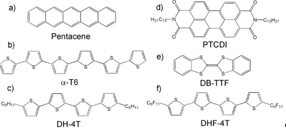
9 Figure 1.1 shows the chemical structure of some of the low MW most studied
organic semiconductors. They can be classified as linear, two-dimensional fused ring compounds, and heterocyclic oligomers. However, while the design, synthesis, and structure–property relationships of p-type organic semiconductors have been widely investigated n-type oligomeric and are still not fully developed.
Figure 1.1 Small molecule semiconductors, which are commonly known for their hole and electron channel characteristics in field-effect transistors. a) Pentacene, b) hexathiophene, c)
α,ω-dihexyl-quaterthiophene, d)N,N′-ditridecyl-3,4,9,10 perylenetetracarboxylicdiimide, e)dibenzotetrathiafulvalene, f) α,ω-diperfluorohexyl-4T
A number of design rules have guided the search so-called for the n-type semiconductors. In order to be able to inject electrons into the LUMO level from environmentally stable electrodes, such as gold, the LUMO level must be lowered (i.e., increasing the electron affinity) substantially in order to align with the work function of the metal. At the same time, increasing the electron affinity of a semiconducting material also improves its environmental stability, that is, its sensitivity to oxygen and water. On the basis of known n-channel transistors, it was generally assumed that a high electron affinity (at least 3 eV) is necessary to observe
n-channel behavior[17]. This is achieved by taking a known semiconducting core molecule and adding strong electron withdrawing groups such as fluorine, cyano, or diimide moieties. In addition to stability and energetic considerations, the orientation of molecules to each other and the associated transfer integrals of electrons play a role. The best LUMO-LUMO overlap for electron transport may be different from the ideal HOMO-HOMO overlap for hole transport[18,19]. Facchetti et al. showed that the molecular packing in crystalline semiconductors can strongly affect the observation of p- or n-channel characteristics[20,21].
10
1.2 Optical Properties in solid state
Many, but not all, spectral properties of small aggregates and crystals are directly traceable to properties of individual molecules. However the energy of interaction between the molecules weak as it be, impose a communal response upon the molecular behavior in the aggregates, the collective response is embodied in an entity called exciton. Excitons represent bound electron–hole pairs, that may be generated by absorption of light or by relaxation of free electrons and holes after optical or electrical pumping. Among the optical properties of exciton systems that have aroused much interest, are cooperative spontaneous emission[22,23] (including
application in light-emitting diodes[24] and lasers[25]), strong optical nonlinearities[26– 28]
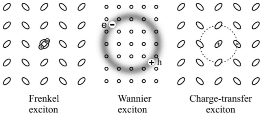
, and optical bistability[29]. Excitons are usually distinguished in two classes:
Frenkel excitons and Wannier–Mott excitons[30] (Figure 1.2). The distinction lies in the typical separation between electron and hole. For Frenkel excitons, this separation is essentially zero (electron and hole occur on the same molecule or atom) and their binding energy is large (~1 eV). For the Wannier–Mott exciton the electron–hole separation is much larger than a single molecule or atom and the binding energy is small (~1 meV). Physically, the distinction originates from the competition between two energy scales: the electron–hole coupling and the rates for electron and hole hopping between different molecules or atoms[31].
Figure 1.2 Classification of excitons on the basis of the electron-hole pair radius.
While the names Frenkel and Wannier–Mott excitons refer to two extreme cases with regards to the length scale of relative electron–hole motion (the internal exciton structure), this scale in practice does allow for all the intermediate cases. The intermediate case that has acquired a special status is the charge-transfer exciton
11 CTE, which in its lowest-energy variation has an electron–hole separation of one
molecule. Thus, the hole is located at one molecule and the electron on the neighboring one. This is often referred to as a “donor–acceptor (D-A) complex”. CTEs may occur in systems with an alternating structure of two types of molecules [16], but also in crystals with just one type of molecule (such as anthracene,
naphthalene, and many others). In the latter case, any molecule in the crystal can
play the role of donor or acceptor. CTEs currently are considered important intermediate states in the photo-conductivity of organic crystals[32]. In this process, they are essential in the creation of free carriers from photo-generated Frenkel excitons.
1.2.1 Excitons in molecular crystals
To account for the dependence of spectroscopic properties on the molecular organization imposed by the solid state, molecular exciton theory has been developed.[33−35] The theory takes into account coupling between transition charge densities associated with transitions between the ground state and singlet excited states localized on individual molecules within the crystal. This coupling results in the formation of delocalized excited states and collective spectroscopic transitions. In crystals containing only one molecule in the unit cell, a positive interaction energy between the transition charge densities of the individual molecules results in a collective spectroscopic transition that occurs at a photon energy higher than the corresponding transition of the isolated molecules. Molecular assemblies showing such a hypsochromically shifted absorption band are commonly referred to as H-aggregates[36]. Conversely if the interaction energy is negative, a collective transition is predicted at photon energies lower than that for the corresponding isolated molecules. Molecular assemblies with such red-shifted absorption bands are classified as J-aggregates. Transition to the upper state is allowed in molecules with cofacial arrangement (H-aggregates) and transition to the lower state is allowed in molecules arranged in head to tail fashion (J-aggregates) Figure 1.3
12 Figure 1.3 Schematic representation of exciton splitting W of the optically allowed transitions and the
splitting energy between excited states both in H- and J-aggregates.
J-aggregates are the only molecular systems where electronic excitation is delocalized over several molecular units as a result of significant retention of π-overlap between neighboring molecules, giving rise to many cooperative and coherent phenomena, such as giant oscillator strength and superradiance, making such systems strongly emissive[ 37]. π-Conjugated materials with such orientations can form ideal candidates for optoelectronic devices because they combine both high luminescence and charge-conducting properties of organic molecules.
For crystal structures with n molecules in the unit cell, the maximum number of allowed collective transitions equals n. For crystal structures with two molecules in the unit cell, which is common for aromatic molecules, two optically allowed electronic transitions are expected. Such molecular assemblies can in principle show both J- and H-type bands. The difference in photon energy between the two allowed transitions is referred to as the Davydov splitting (DS). The DS may be regarded as an experimental observable. In doing so, it is important to note that the splitting is not completely determined by the electronic motion. It can also be influenced by motion of the atomic nuclei, especially in the case where the coupling between electronic and vibrational degrees of freedom is strong in comparison to the strength of the excited-state intermolecular electronic coupling. Depending on the particular material and vibronic band under study, the magnitude of the DS can be strongly reduced by the included Franck−Condon factors, accounting for the overlap between vibrational wave functions at ground and excited states. The DS is also influenced by charge transfer interactions between (neighboring) molecules[38].
13
1.3.1 Exciton generation, diffusion and relaxation
In the previous sections we have shown how the isolated molecule energy levels split to form the exciton band and the Davydov components in a molecular solid. Here we describe how an exciton can be created and discuss the processes it may undergo upon diffusion and relaxation.
Exciton generation
An exciton can be generated exciting the crystal or the thin film with an electromagnetic wave. This light must have a frequency resonant with the energy gap and the right polarization with respect to the transition dipole moments. Moreover, in order to have light absorption and exciton creation optical selection rules must be satisfied. In particular, the photon momentum q must be equal to the k wave vector. Since in the UV/VIS region q ~ 0, only k = 0 states are probed. If the crystal has an inversion center then states are classified as gerade (g) and ungerade (u) and only u ← g transition are allowed. Two photon absorption (i.e. absorption of light through a mid gap virtual state), being a second order process, is capable to perform g ← g transitions[39]. An electrical way to generate excitons is by charge carrier recombination. This process involves: the injection of holes and electrons in the material by means of electrodes, their diffusion in the presence of an electric field, charge recombination and exciton formation. In this case both triplet and singlet exciton are created with a ratio 3/1, respectively. Light emission of electrically generated exciton is called electroluminescence and in organic semiconductors was first observed by Pope[40]. Electroluminescence is at the basis of the operation of optoelectronic devices such as OLED[41] and OLET[42].
Exciton diffusion
As pointed out in the definition of exciton, this quasiparticle is characterized by a wave-like motion. This aspect is relevant not only from the fundamental viewpoint of the energy transport but also because of its importance for optimal design of organic thin film electronic device. Immediately after exciton creation, the phases of the wfs of all excited molecules have a unique relationship. If the phases are maintained during the excitation motion, the exciton moves as a wave and is said to be coherent. However, because of the interactions with lattice modes (phonons) and imperfections
14 (physical and chemical) in the crystal the coherence may be lost. Then the exciton
moves with a random hoppinglike behavior. Typical values of the exciton diffusion coefficients for single crystals are 10−3 ÷ 10−5 cm2 sec−1. During the hopping movement, excitons can experience sites with an energy below the exciton band. In this case, if the thermal energy is not sufficient to promote the hopping, the exciton is trapped. Then it can relax with emission of radiation or with a non radiative pathway. We neglect here the treatment on high exciton density phenomena such as exciton-exciton annihilation or exciton-exciton-polaron interactions since they are not relevant for the experimental results reported in this thesis. A detailed review of these processes in organic semiconductor can be found in reference [i1].
Exciton relaxation
There are many pathways that an exciton can undergo in order to relax to the fundamental ground state. The investigation of the energetics and the dynamics involved in these processes is the fundamental question of solid state photophysics. Since this thesis focuses on the photophysical properties of T4DIM in the solid state, we will discuss in detail all the processes relevant for this material, though with a general approach. Figure 1.4 show an energy diagram of the different relaxation pathway for an exciton.
Figure1.4 Energy diagram for a molecular solid with two Davydov components, a charge transfer state and a relaxed state. Upward arrow show the absorption of light with an energy matching the higher Davydov band. Thick bend arrows show the exciton hopping between adjacent molecular sites. Curved downward arrows show nonradiative processes while straight downward arrows represent radiative processes.
15 Initially, light with a resonant frequency is absorbed and an exciton is created in the
upper or lower Davydov component (upward arrow) according to frequency and polarization. Few hundred of femtoseconds later the exciton can either relax to the lowest Davydov component (curved arrow) or it can hop to the nearest sites (thick bend arrow) and eventually dissociate to form a charge transfer state. All these early stage processes are non radiative and are usually probed with ultrafast pump and probe spectroscopies[43]. It is important to point out here that, due to the Kasha rule, radiative relaxation always takes place from the lowest state of the exciton band. As a consequence, we expect light emission from the lowest excitonic level and eventually from ”relaxed states” that lie just below the exciton band. In Figure 1.4 it is shown that is possible to observe fluorescence (downward arrow) from the above mentioned states and eventually phosphorescence (oblique arrow) from triplet exciton states. All the transitions illustrated in Figure x are characterized by a rate constant k that is the sum of at least two components k = kr + knr. In the case of fluorescence the measured lifetime is the reciprocal of k. In order to obtain kr equation can be used provided that the fluorescence quantum yield (ΦF ) is known. kr
= ΦF k In this thesis we will use the term photoluminescence (PL) as a synonymous
of fluorescence.
1.3 Electrical Properties.
For an organic semiconductor the key quantity that characterizes charge transport is the carrier mobility. Although these do not directly concern with the experiments and with the results reported in this thesis, it is important to have an overview of all the physical/chemical properties of organic semiconductors. In the absence of any external potential, transport is purely diffusive and is generally described by a simple diffusion equation:
where denotes the mean-square displacement of the charges, D is the diffusion coefficient, t is the time, and n represents an integer number equal to 2, 4, or 6 for one-, two-, and three-dimensional (1D, 2D, and 3D) systems, respectively.
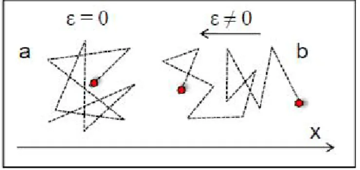
As one applies an electric field to a semiconductor, the electrostatic force causes the carriers to first accelerate and then reach a constant average velocity, v, due to collisions with impurities and lattice vibrations. The ratio of the velocity to the
16 applied field is called the mobility. Diffusion should be seen as a local displacement
of the charge around an average position, while drift induces a displacement of the average position. Drift is the effect that dominates the migration of the charges across an organic layer in the devices. The carrier mobility is usually expressed in
cm2/V·s (since it corresponds to velocity over electric filed) Figure 1.5.
Figure 1.5 The carrier motion in the semiconductor in the absence and in the presence of an electric field.
It is natural to imagine the process of charge transport in a organic semiconductor as a series of redox events, where the charge residing on one molecule is transferred to the next one as in the scheme below, valid for one dimensional chain of identical molecules where an electron has been removed:
…AA+AA… → …AAA+A…
The charge mobility so can be described by sequential hopping between molecules and the maximum value can be express in terms of physical quantities that are all experimentally accessible. The evaluation of the maximum hopping mobility with realistic parameters suggest that sequential charge hopping is not the correct transport mechanism for the best molecular material used in organic transistor[44]. The simple hopping transport model, made very common in the chemistry by its simplicity and by analogy with redox chemistry, is in practice never valid for the hights crystalline material. The exact nature of charge transport in organic semiconductors is still open to debate. Nevertheless, one can make a clear distinction between disordered semiconductors such as amorphous polymers and highly ordered organic single crystals, at the opposite ends of the spectrum. Charge transport in disordered semiconductors is generally described by thermally activated hopping of charges through a distribution of localized states or shallow traps. For highly ordered molecular crystals such as, e.g., rubrene, tetracene, and pentacene, however,
17 experimental data seems to exclude hopping transport. Temperature-dependent
time-of-flight[67] and time-resolved terahertz pulse spectroscopy[46,47], measurements on high purity crystals showing high mobilities that increase with decreasing temperature, suggest bandlike transport in delocalized states instead of hopping transport. Models for charge transport in organic semiconductors, such as polycrystalline thin films of small molecules and microcrystalline polymers that lie in between these two extreme cases, have been proposed as well[48-50]. Note that in all cases the transfer integral representing the electronic coupling of adjacent molecules and the polaronic relaxation energy, which is the energy gained when a charge geometrically relaxes over a single molecule or polymer segment, is an important parameter determining the probability of charge transport from one molecule to another and depends strongly on the particular molecule and the relative position of the interacting units.
1.4 Overview on OLETs devices
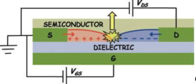
Organic Light-Emitting Field-Effect transistors (OLETs) are emerging as an innovative class of multifunctional devices that integrates the electronic properties of a transistor, the light generation capability and the full potential of organic photonics. The most advanced OLET structures encompass a huge technological potential for the realization of intense nanoscale light sources and highly integrated optoelectronic multifunctional systems. As for a traditional field-effect transistor (organic or
inorganic) an OLET device requires the following components (shown in Figure 1.6): a thin semiconducting layer, which is separated from a gate electrode by the
insulating gate dielectric; source and drain electrodes of width W (channel width) separated by a distance L (channel length) that are in contact with the semiconducting layer.
Figure 1.6 Schematic of an organic light-emitting field-effect transistor with the constituent components.
18 In an ambipolar transistor both holes and electrons are simultaneously injected in the
channel by the source and drain electrodes at a suitable gate bias that has to be higher in absolute value with respect to the hole and electron gate threshold voltages. In the case of ideal ambipolar transistor with only one semiconducting layer, the ambipolar regime is characterized by a hole and an electron accumulation layer that meet at some point within the transistor channel. The position of the electroluminescence emission region is moved within the channel according to the applied gate and source-drain voltages and the charge-carrier mobility ratio. So, the micrometer separation between the emission area and the injecting electrodes in ambipolar OLETs leads to improved emission quantum efficiency due to the decreased photon losses.Most of the single-layer organic field-effect transistors that have been fabricated to date show only unipolar conduction (either holes or electrons) even though in principle pure organic semiconductor should support both electron and hole transport equally[51].Given the limited number of electroluminescent materials with good ambipolar mobility values, different device architectures are to be implemented to achieve high ambipolar transport in OLETs
1.4.1 Working Principle of OFETs
Since throughout this thesis we deal only with bottom gate-top contact configuration (Figure x), we use this simple configuration to discuss briefly how a classic OFET works. We refer to the voltage applied between drain and source as Vds, while the voltage applied to the gate is labeled as Vgs. By convention, the source is generally
considered grounded and the voltage is applied to the drain contact. The current flowing through the channel is called Ids and it is a strong function of Vgs. The
dielectric is sandwiched between the gate and the organic semiconductor, and they work as two plates of a plane capacitor. Thus, when a Vgs is applied, charges of
different sign are accumulated at gate/dielectric and dielectric/organic semiconductor interfaces. Much of this accumulated charge in the active material is mobile and moves in response to the applied Vds. When no Vgs is applied there are ideally no free
charge carriers, and the device is off. Otherwise, with applied Vgs the device is on.
19 of the working principle of FETs[52]. An n-channel OFET (i.e., electrons are
transported through the channel) can be used as an example to understand the basic device operational regimes due to the gate voltage dependence of the distribution of ”free” charges in the active material[53]. If we assume ohmic contacts and no trap presence (ideal case), when a Vgs > 0 is applied, free electrons start accumulating at
organic semiconductor/dielectric interface. Without any voltage difference between drain and source (Vds = 0), this negative charge density is uniform along all the active
material, thus having a uniform conduction channel. If a positive Vds is applied, the
induced charge superficial density in a certain position x of the semiconductor is described by Eq. (1):
qind = n(x)et = Ci [Vgs − V (x)] (Eq.1)
where t is the thickness of the charge layer in the channel, n(x) is the number density of charges in the channel, e is the electron charge and Ci is the insulator capacitance
per area unit. However, real devices are far from being ideal and not all induced charges are mobile; a large number of deep charge traps are present in the film (deep enough to effectively immobilize electrons trapped in them). Deep traps have to be filled before the additionally induced charge can move. Thus, a minimum gate voltage has to be applied to obtain free electron density in the channel, the threshold voltage, Vth. If we include the threshold voltage in the previous equation:
qind = n(x)et = Ci [Vg − Vth − V (x)] (Eq.2)
As Vth is not ideally a function of x, with Vds = 0 and Vgs > Vth a homogeneous charge
density is present in the channel. When a small source-drain voltage is applied (Vds
<< Vgs − Vth) a linear gradient of charge density is formed. The voltage drop
between organic semiconductor and gate is larger at the source, where V (x) = 0 (grounded), than at the drain, where V (x) = Vds. This is the linear regime in which the current flowing through the channel is directly proportional to Vds (Figure1.7a).
When the source-drain voltage is further increased, we reach a point where a potential difference between the gate and the part of the channel near the drain no longer exists, the channel is pinched off. This means that a charge carrier depletion region is formed next to the drain, because the difference between the local potential
V (x) and Vgs is lower than the threshold voltage. A space-charged-limited saturation
current can flow across this narrow depletion zone. Carriers are swept from the pinch point to the drain by a comparatively high electric field in the depletion region (Figure 1.7b). A further increase in Vds pushes the pinch-off point further away from
20 the drain (Figure 1.7c). However the length of the channel (L) shortens only slightly,
as it is infinitely larger than the width of the depletion region, and the integrated resistance of the channel from the source to the pinch point remains more or less the same.
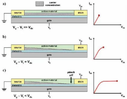
Figure 1.7. Schematic structure of an OFET. a) Carrier concentration profile in the linear regime; b) Carrier concentration profile when the pinch off occurs near the drain electrode (Vgs–Vth=Vds); c) Carrier concentration profile in the saturation regime.
For these reasons once pinch off condition is met, current saturates at Isatds . From a
mathematical point of view, pinch off is reached when Vds = Vgs−Vth. The
current-voltage characteristics in the different operating regimes of an OFET can be described analytically, in a simplistic way assuming that (1) the transverse electric field induced by the gate voltage is largely higher than the longitudinal field induced by the gate bias (gradual channel approximation) and (2) the mobility is constant all over the channel. In short, current-voltage characteristics can be drawn by either varying the drain voltage at a constant gate voltage (output characteristics) or changing the gate voltage at a fixed drain voltage (transfer characteristics). Locus characteristics are obtained by varying simultaneously drain voltage and gate voltage and keeping them at the same value so that the pinch-off condition is always reached in the reached the drain electrode. In the output characteristics, the curves are divided into a linear regime at low Vds that turns into the saturation regime when Vds > Vgs.
21 in which µ is the charge carrier mobility.
References
[15] (a) Organic Electronic Material: Conjugated Polymers and Low Molecular
Weight Organic Solids (Eds: R. Farchioni, G. Grosso) Springer, Berlin 2011. (b) S.R.
Forrest, Nature 2004, 428,911 (c) T.W.Kelly, et al. Chem. Mater. 2004, 16, 4413. [16] Printed Organic And Molecular Electronics ( Eds: D.Gamota, P.Brazis, K.Kalyanasundaram, J.Zhang), Kluwer Academic, Boston, MA 2004.
[17] Bernius, M. T.; Inbasekaran, M.; O’Brien, J.; Wu, W. S. AdV. Mater. (2000),
12, 1737.
[18] Becker, H.; Spreitzer, H.; Kreuder, W.; Kluge, E.; Schenk, H.; Parker, I.; Cao, Y. AdV. Mater. (2000), 12, 42.
[19] Jurchescu, O. D.; Baas, J.; Palstra, T. T. M. Appl. Phys. Lett. (2004), 84, 3061. [20] Chua, L. L.; Zaumseil, J.; Chang, J. F.; Ou, E. C. W.; Ho, P. K. H.; Sirringhaus, H. R.; Friend, H. Nature (2005), 434, 194.
[21] Dimitrakopoulos, C. D.; Malenfant, P. R. L. AdV. Mater.(2002), 14, 99.
[22] M. Kasha, in: B. di Bartolo (Ed.), Spectroscopy of the Excited State, Vol. B12, Plenum, NewYork, (1976).
[23] S. de Boer, K. Vink, D.A. Wiersma, Chem. Phys. Lett. 137 (1987) 99.
[24] N.C. Greenham, S.C. Moratti, D.D.C. Bradley, R.H. Friend, A.B. Holmes,
Nature 365 (1993) 628.
[25] U. Lemmer, A. Haugeneder, C. Kallinger, J. Feldmann, in: G. Hadziioannou, P.F. van Hutten (Eds.), Semiconducting Polymers, Wiley-VCH, Weinheim, (2000). [26] B.I. Greene, J. Orenstein, S. Schmitt-Rink, Science 247 (1990) 679.
[27] V.L. Bogdanov, E.N. Viktorova, S.V. Kulya, A.S. Spiro, Pis’ma Zh. Èksper.
Teoret. Fiz. 53 (1990) 100; JETP Lett. 53 (1991) 105.
[28] Y. Wang, J. Opt. Soc. Amer. B 8 (1991) 981.
[29] H.M. Gibbs, Optical Bistability: Controling Light with Light, Academic Press, New York, (1985).
22 [31] H. Haken, Quantum Field Theory of Solids: An Introduction, North-Holland,
Amsterdam, 1976.
[32] M. Pope, C.E. Swenberg, Electronic Processes in Organic Crystals and Polymers, Oxford University Press, Oxford, (1999).
[33] Davidov, A. S. Theory of Molecular Excitons; Plenum Press: New York, (1971). [34] Philpott, M. R. Some Modern Aspects of Exciton Theory. In Advances in Chemistry and Physics; Prigogine, I., Rice, S. A., Eds.; J.Wiley: Hoboken, NJ, (1973); Vol. 23.
[35] Agranovich, V. M. Excitations in Organic Solids; Oxford University Press: Oxford, U.K., (2009).
[36] Spano, F. C. Acc. Chem. Res. (2010), 43, 429−439.
[37] Da Como, E.; Loi, M. A.; Murgia, M.; Zamboni, R.; Muccini, M. J-Aggregation in R-Sexithiophene Submonolayer Films on Silicon Dioxide. J. Am. Chem. Soc. 2006, 128, 4277–4281
[38] Yamagata, H.; Norton, J.; Hontz, E.; Oliver, Y.; Beljonne, D.; Brédas, J. L.; Silbey, R. J.; Spano, F. C. J. Chem. Phys. (2011), 134, 204703 1−11.
[39] N. Periasamy, D. Danieli, G. Ruani, R. Zamboni, and C. Taliani, “Location of the low-energy Ag1 state in a polythiophene oligomer by 2- photon absorption-spectroscopy: alpha-sexithienyl,” Phys. Rev. Lett., vol. 68, pp. 919–922, 1992.
[40] M. Pope, H. Kallmann, and P. Magnante, “Electroluminescence in organic crystals,” J. Chem. Phys., vol. 38, pp. 2042–2043, 1963.
[41] S. R. Forrest, “Ultrathin organic films grown by organic molecular beam deposition and related techniques,” Chem. Rev., vol. 97, pp. 1793–1896, 1997.
[42] C. Rost, S. Karg, W. Riess, M. A. Loi, M. Murgia, and M. Muccini, “Ambipolar light-emitting organic field-effect transistor,” Appl. Phys. Lett., vol. 85, pp. 1613– 1615, 2004.
[43] G. Lanzani, S. V. Frolov, P. A. Lane, Z. V. Vardeny, M. Nisoli, and S. De Silvestri, “Transient spectroscopy of Frenkel and charge transfer excitons in alpha-sexithienyl films,” Phys. Rev. Lett., vol. 79, pp. 3066 – 3069, (1997).
[44] A. Troisi, Organic Electronics 2011, 12, 1988-1991
[45] Warta, W.; Stehle, R.; Karl, N. Appl. Phys. A: Mater. Sci. Process. (1985), 36, 163.
[46] Ostroverkhova, O.; Cooke, D. G.; Shcherbyna, S.; Egerton, R. F.; Hegmann, F. A.; Tykwinski, R. R.; Anthony, J. E. Phys. ReV. B (2005), 71, 035204.
23 [47] Ostroverkhova, O.; Cooke, D. G.; Hegmann, F. A.; Anthony, J. E.;
Podzorov, V.; Gershenson, M. E.; Jurchescu, O. D.; Palstra, T. T. M. Appl. Phys.
Lett.(2006), 88, 162101.
[48] Horowitz, G. J. Mater. Res.(2004), 19, 1946. [49] Sirringhaus, H. AdV. Mater. (2005), 17, 2411.
[50] Salleo, A.; Chen, T. W.; Volkel, A. R.; Wu, Y.; Liu, P.; Ong, B. S.; Street, R. A.
Phys. ReV. B (2004), 70, 115311.
[51] N. Karl, Synth. Mater. 133–134, 649 (2003).
[52] C. R. Newman, C. D. Frisbie, D. A. da Silva Filho, J. L. Bredas, P. C. Ewbank, and K. R. Mann. Introduction to organic thin film transistors and design of n-channel organic semiconductors. Chem. Mater., 16:4436–4451, (2004).
[53] J. Zaumseil and H. Sirringhaus. Electron and ambipolar transport in organic field-effect transistors. Chem. Rev., 107(4):1296, (2007).
24
Chapter 2
Experimental setup
In this chapter a description of the experimental setups used to prepare thin films of T4DIM and to perform steady state photoluminescence at low temperature, time resolved PL spectroscopy and quantum yield measurements are reported. The chapter includes also a brief introduction to optical microscopy and an overview on atomic force microscopy.
2.1 Quantum yield measurement.
The external radiative quantum efficiency, η, is defined by Equation 5.
η = (number of photons emitted) / (number of photons absorbed) (Eq.5) PL efficiency measurements in solution are relatively simple because it is usually appropriate to assume an isotropic angular distribution for the emission. However, this is not true for thin solid films. For molecular and polymeric materials, anisotropy in the distribution of chromophores leads to an anisotropy in the emission dipole-moment. In addition, wave-guiding effects also modify the angular distribution of the emission. A summary of the traditional methods for measuring η has been given by Demas[54]. A popular method is the comparison of fluorescence emission spectra from two solutions one of which is a standard. Quantum yield measurement with
Integrating Sphere of anisotropic films were first discussed by DeMello[55]. An integrating sphere is a hollow sphere which has its inner surface coated with a diffusely reflecting material (typically barium sulfate). When a light source is placed in an ideal integrating sphere, the light is redistributed isotropically over the sphere interior-surface regardless of the angular dependence of the emission[56].Hence, if NΩ
photons are detected over a solid-angle Ω, the total number of photons emitted, N, is given by Equation 6.
25 N = NΩ(4π/η) (Eq.6)
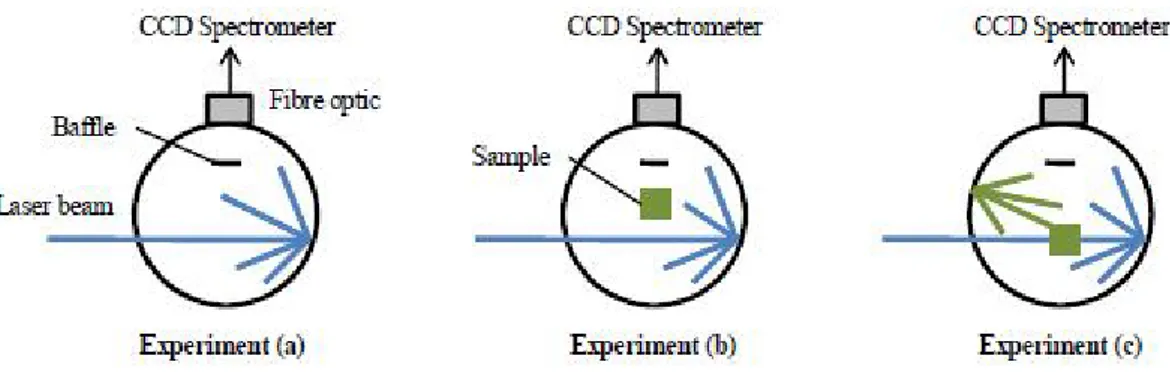
The basic experimental set up is shown in Figure 2.1. An optical fiber leads from the wall of the sphere to a grating spectrometer with a CCD. Immediately in front of the optical fiber is a baffle coated with barium sulfate to prevent direct illumination of the optical fiber. Laser illumination of appropriate wavelength is directed into the sphere through a small entrance hole. Three measurements are made using the sphere. For the first measurement, Figure 2.1a, the sphere is empty and laser light alone is detected by the spectrometer. For the second measurement, Figure 2.1b, the sample is placed inside the sphere and the laser beam is directed on to the sphere wall. The third measurement, Figure 2.1c, is similar to the second, except that the collimated laser beam is now directed on to the sample (the sample is oriented such that laser light reflected from the surface of the sample is directed onto the sphere wall and not back through the entrance hole).
Figure 2.1 Diagram illustrating the three configurations of the sphere required for the efficiency measurement: a) the sphere is empty: b) the sample is in place and the laser beam is directed onto the sphere wall; c) the sample is in place and the laser beam is directed onto the sample.
The total amount of laser light striking the sample can be separated into two contributions. The first is the incident laser beam which strikes the sample directly and locally. The second is diffuse laser light which has scattered from the wall of the sphere and subsequently strikes the sample over its entire surface. After these measurements the value of the quantum yield is given by follow Equation 7 :
where La, Lb and Lc are the intensities of the laser beam during the three
measurement mentioned above, while Pb and Pc are the intensity related to the photoluminescence of the sample in the experiments b and c respectivately.
26
2.2 Steady State Photoluminescence at low temperature
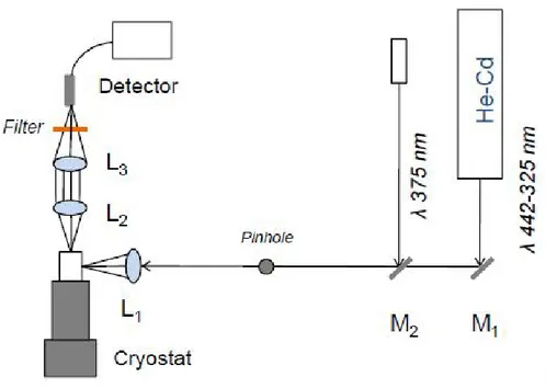
Photoluminescence (PL) is the spontaneous emission of light from a material under optical excitation. The excitation energy and intensity are chosen to probe different regions and excitation concentrations in the sample. In organic semiconductor systems, the most common radiative transition is between the HOMO-LUMOstates, with the energy difference being known as the bandgap. The basic elements of a PL spectroscopy set-up consist in an optical source, a sample holder and a photonic multichannel analyzer (PMA). The PMA is a compact spectral measurement apparatus that combines a spectrometer and optical detector into one unit. In our measurement we used as optical source a He-Cd laser that is capable of producing both a UV and visible light at 325 and 442 nm respectively and a diode laser at 375nm wavelength excitation.
Figure 2.2 Schematic diagram for PL measurements at low temperature.
A typical PL set-up is shown in Figure 2.2 The easiest way to describe the optics of the experiment is to follow the light beam. As it leaves the laser, a mirror are used for alignment the beam through a pinhole that improves the uniformity and the power of the beam. Then the excitation laser beam is focused on the sample with a lens L1 of typically f=20-30 cm focal length. The emitted light can be collected by two plano-convex achromatic lenses L2 and L3. An achromatic lens, also referred to as an
27 achromat, typically consists of two optical components cemented together, usually a
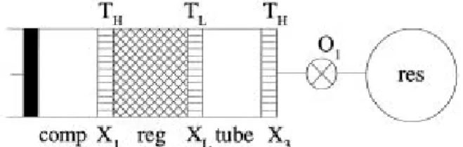
positive low-index (crown) element and a negative high-index (flint) element. This design permits an improvement in performance because the chromatic aberration of one is counterbalanced by that of the other. The combination of the two lenses L2 and L3 each working at infinite conjugation ratio, but with the convex surface toward the focus, has the advantage to reduce the spherical aberration. Moreover in order to improve the collection efficiency of the emitted light a short focal length for L2 lens is used. While, L3 can be chosen in order to match the optical aperture of the detector, avoiding unnecessary supplementary losses. For PL measurement at low temperature the sample holder is a vacuum cryogenic pump with high refrigerating capacity in the range of 6 to 320 K. A schematic description of that system is given in Figure 2.3. From left to right it consists of: a compressor at room temperature and three heat exchangers X1 (which dumps heat to room temperature TH), XL at the low
temperature TL (which absorbs the useful cooling power QL) and X3 (rejecting heat
to room temperature). Then a regenerator (which contains a porous matrix that absorbs heat from the gas when it flows to the right, and gives off the heat again when it flows to the left), a tube (which is basically noting more than a tube in which the gas moves back and forth), and orifice O1 (in principle this is a pure flow resistance adjusted to give the optimum performance). The working medium usually is helium. An extensive explanation of the operation of PTRs is given in[57].
Figure 2.3 Schematic diagram of a Stirling-type single inlet pulse tube refrigerator.
The compressor generates a pressure P in the system which varies periodically in time. The cooling at the cold heat exchanger XL takes place due to the fact that the gas leaves the heat exchanger to the right with a temperature TL and comes back with a temperature lower than TL. Typically, the pressures are in the 10-20 bar region. The pressure varies rather smoothly with time and usually the gas velocities are small.
28
2.3 Ti:sapphire laser
Ti:sapphire mode-locked lasers provide a large wavelength tuning range, from about 690 to over 1050 nanometers, with pulse widths approximately 100 femtoseconds in length. Note that the lowest pulse width attainable in the actual Spectra Physics laser is 50 femtoseconds. In addition, these lasers have sufficient power (greater than 100 milliwatts throughout the tuning range) for saturation of two-photon excitation in most fluorophores. To ensure proper cooling and humidity control of the laser crystal, nitrogen gas is pumped into the sealed laser head, which is maintained at constant temperature by an external chiller.
The Titanium trivalent cation is responsible for laser action in doped sapphire crystals, which are produced by introducing titanium oxide into a melt of aluminum oxide. In the melt, some of the titanium ions diffuse into the aluminum oxide and are incorporated into lattice positions in place of aluminum cations. When excited by the argon-ion pump laser, titanium atoms in doped sapphire crystals absorb the greenish-blue light, which is subsequently released as coherent infrared light via stimulated emission. As the emitted light is repeatedly reflected back through the crystal with mirrors, it is amplified until laser oscillation occurs. Ti:sapphire lasers require a supporting pump laser of sufficient power to excite the crystal and initiate laser action. Power requirements vary with output demand, but strongly focused argon-ion lasers having values between 5 and 20 watts can be utilized for this purpose. Recently, new solid state lasers have been developed that employ nonlinear conversion to double the output frequency of infrared lasers to produce lower wavelength green light. These lasers are far more efficient than argon-ion lasers and also have reduced power and cooling demands.
29
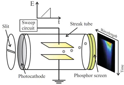
2.4 Streak camera
A Streak camera is an optoelectronic device used to observe light emission phenomena occurring on the sub-nanosecond time scale. Together with the TCSPCis one of the most widely used technique to record PL time decays.
Streak cameras building blocks are: - Photocathode
- Streak tube
- Image recording device (CCD)
A scheme of the device with the main parts is illustrated in Figure 2.4. The operating principle can be explained considering a light pulse with a certain time profile f(t). When the light impinges the photocathode a proportional amount of electrons is emitted and is accelerated across the streak tube. In the streak tube two parallel deflection plates are settled.
Figure 2.4 Scheme of the streak camera. The slit selects the photons that impinge on the photocathode. The photocathode converts photons into electrons. Inside the streak tube two plates are used to deflect electrons according to the voltage ramp applied by the sweep circuit. The phosphor screen converts electron into photons. Photons are recorded with the CCD (not shown) placed after the phosphor screen.
In synchrony with the arrival of electrons a rising voltage ramp is applied to the plates. Electrons that first enter the tube are deflected very little, since the value of the electric field (E) is low. Electrons which enter later are further deflected, because of the increased field. In this way the original light pulse f(t) is swept in space f(y) as a streak in the direction y, that is parallel to the electric field. At the tube end a phosphor screen converts electrons back to photons that are recorded as an image by
30 a CCD. The resulting data are obtained as an image in which the y axis represents
time and x the wavelength if a spectrograph is coupled in front of the photocathode at the entrance slit. In the right part of Figure 2.4, a typical streak image with the PL intensity reported in false color it is shown. In our setup a spectrograph with three different gratings (50 g/mm, 100 g/mm and 1200 g/mm) is used to disperse the wavelength along the x axis before entering the horizontal slit. Spectral resolution for the three different gratings is: 17 meV, 10 meV and 0.8 meV respectively. In the Streak camera the arrival of light pulses and the sweep of the electric field must be synchronized with a trigger. The optical trigger used for this purpose is shown in figure 2.3 and consists of a fast PIN diode that drives the sweep circuit according to the Ti:sapphire repetition rate (~ 80 MHz). The temporal resolution of the streak camera employed in the setup of figure 1.3 is 1.9 ps. However, this is the so called one-shot resolution. The actual time resolution during signal integration is larger. In particular, the unremovable time jittering of the streak camera during integration is responsible for a time resolution of 5 ps. Exhaustive reviews on streak cameras can be found in references[59, 60].
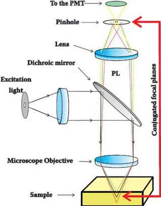
2.2.1 Confocal Laser Scanning Microscopy (CLSM)
Conventional optical microscopy uses extended light sources to illuminate all the sample field of view at the same time to create a magnified image, viewed by eyes or by an extended detector. In confocal microscopy light from a point source probes a very small region and a point detector ensures that only light from the very same small area is detected. For this purpose a point detector must be located in a plane conjugated (confocality) with the point source. Figure 2.5 shows a simplified scheme of the working principle of a confocal microscope. The spatial filter (pinhole) ensures that the detector is practically point-like. In the figure only the PL (colored lines) from the focal plane of the sample is focused on the detector (PMT4). Thus
confocal microscopy is able to reject features that are out of focus. Confocal
microscopy has two main advantages with respect to conventional microscopy: - Optical sectioning and 3-D reconstruction of translucent specimens.
31 Spatial resolution is one of the most desired features of every microscope. The
resolution can be measured or calculated considering the FWHM of the image of a sub-resolved point object. This image is usually called pointspread function (PSF).
Figure 2.5 Schematic diagram illustrating the operation principle of a confocal microscope. The excitation light is reflected by a dichroic mirror and focused by the objective, the sample PL (colored lines) is recollected by the objective and focused on the pinhole that prevents the out of focus PL rays (dotted lines) to reach the detector.
Table 2.1 lists the spatial in plane (x-y) and axial (z) resolution for different optical
microscopy techniques. Note that resolution is expressed as a function of the wavelength of light, considering an objective with NA = 1.4 for the far field techniques (i.e. Optical and Confocal microscopy) and a pinhole of null size for the confocal microscope. The resolution values reported in table 2.1 refer to the case in which light of the same wavelength λ is used to illuminate the sample and to reconstruct the optical image. When the light arising from PL is detected, two different wavelength are involved in the process of image formation: λ1 is used to excite the sample and λ2 is the longer PL wavelength used to form the image. In order to take this into account, values reported in table 2.1 for confocal microscopy are linearly dependent on a factor β that is defined as β= λ2/λ1. Even if it is practically impossible to work with β = 1, this value represents the ideal limit once the exciting wavelength λ1 is fixed.
32 Optical Microscopy Confocal Microscopy
x-y resolution 0.436λ 0.31λ
z resolution 2λ 0.46λ
Table 2.1 In plane (x-y) and axial (z) resolution for conventional optical microscopy and confocal microscopy.
Since in confocal microscopy only a diffraction limited point is imaged, the sample or the light must be scanned in order to obtain an image of the desired field of view. It has been demonstrated that sample scanning confocal microscopy has a better resolution than laser scanning[62]. However, the latter allows obtaining fast imaging without sample degradation ad has found a wider diffusion in commercial instruments. The scan of the exciting laser beam can be accomplished with scanning galvanometric mirrors. In Figure 2.6 a schematic drawing of a scanning head for confocal microscopy is shown. The exciting laser beam is illustrated as a continuous line and is scanned by two galvanometric mirrors. PL is represented by the dotted line. The confocal PL image of the studied sample is reconstructed by the microscope software, collecting the PL point by point.
Figure 2.6 Schematic drawing of a laser scanning head: Excitation laser beam (continuous line) is reflected by the dichroic mirror and is scanned on the sample surface by the galvanometric mirrors. PL is collected through the same optical path, it passes the dichroic mirror, the pinhole and reaches the detector
33
2.2.2 Atomic Force Microscopy
Atomic force microscopy (AFM) belongs to the family of the Scanning Probe Microscopy (SPM) techniques. SPM are based on 3-D scanning of a sample surface, through a probe which locally interacts with the surface[63, 64] . The probe is placed near the surface (d < 100 nm). An electronic system measures the surfaceprobe interaction at every (x,y) point in the sample[65] . The probe is moved on top of the sample by a piezoelectric actuator, in order to cover a path called raster. The interaction strength (whatever its nature is, depending on the SPM techniques) depends on the sample-probe distance. By mapping the strength in the (x,y) points, we could obtain an image of the sample surface. AFM was invented by G. Binning, C. Gerber and C. Quate[66] . It overcomes the limits of other SPM (like Scanning Tunneling Microscopy, STM) because it permits the analysis of all type of samples (insulator, semiconductor, etc). Furthermore, it allows processing in air, vacuum or liquid environment[67–70].The main components of an AFM are schematically showed in Figure 2.7
• The different interactions (magnetic, electric, etc) settled between the surface and
the probe are strictly dependent on the nature of the probe itself.
• The piezoelectric transducer (also called scanner) which permits probe or sample
movements. Movements are possible in all the three spatial directions with an accuracy in the order of 10−12 m. Vertical movements are guided by a feedback system which keeps the surface-probe interaction fixed. These movements are recorded and used to determine the topological profile of the surface.
Figure 2.7 Scheme of the working principle of the AFM. The scanner moves the sample thereby changing the tip/surface interaction and the optical path of the laser beam, whose movement is collected by a photo-diode.
34 • A mechanical system, to damp the external vibrations; the above mentioned
feedback system for keeping the signal with the physical information at a set value (setpoint).
• A control system for the acquisition and visualization of the data.
In the AFM technique, the probe is a very sharp pyramidal or conical tip fabricated on the edge of a lever called cantilever. When the tip and the surface interact, a force modifies the cantilevers mechanical balance. These change is detected by a laser beam focused on the back of the cantilever (Figure 2.7). The laser beam, after a convenient optical path, reaches a sensor (beam and bounce). During the surface scanning, the sensor (usually a photo-diode) reveals the different laser beam positions that, after a suitable amplification, are used to reproduce the surface topography.
Figure 2.8: Scanning electron micrograph of a micromachined silicon cantilever with an integrated tip pointing in the [001] crystal direction (Wolter et al., 1991).
The probe is the fundamental part of the instrument since it sets the minimal spatial resolution of the AFM. Ideally, it is conceived to be sensitive to a single chemical-physical interaction with the surface. But in practice this in not possible, so fabrication is important to minimize parasite interactions. There are rectangular or triangular shape levers with conic or pyramidal tip. Classic conic tips present these features: length around 100 − 130µm, 35µm wideness, 2µm thickness, tip radius of curvature of 10 nm and an elastic constant less than 10 N/m Figure 2.8. Several forces typically contribute to the deflection of an AFM cantilever. The force most commonly associated with atomic force microscopy is an interatomic force called the van der Waals force. The dependence of the van der Waals force upon the distance between the tip and the sample is shown in Figure 2.9
35 Two distance regimes are labeled on Figure 2.9: (i) the contact regime; and (ii) the
non-contact regime. In the contact regime, the cantilever is held less than a few angstroms from the sample surface, and the inter-atomic force between the cantilever and the sample is repulsive. In the non-contact regime, the cantilever is held on the order of tens to hundreds of angstroms from the sample surface, and the inter-atomic force between the cantilever and sample is attractive (largely a result of the long- range van der Waals interactions).
Figure 2.9 Graph showing the repulsive/attractive forces between the surface and the cantilever as a function of the distance.
A third operation mode has been developed, between the contact and non contact modes: the semi-contact or tapping Mode (Figure 2.10). In Tapping Mode AFM the cantilever is oscillated at or near its resonance frequency with an amplitude ranging typically from 20 to 100 nm. During the scan the tip lightly taps on the sample surface contacting the surface at the bottom of its swing[71, 72]. The feedback loop keeps constant the oscillation amplitude by maintaining a constant root-mean-mean value of the oscillation signal acquired by the split photodiode detector (setpoint).
Figure 2.10: Scheme of the AFM working modalities. In contact mode the topography is obtained by the cantilever bending; in no- contact mode and semi-contact (or tapping) mode the signal comes from the variation of frequency, magnitude and phase of the cantilever oscillation.