low-power neuromorphic networks
Cite as: APL Mater. 7, 081120 (2019); https://doi.org/10.1063/1.5108650Submitted: 30 April 2019 . Accepted: 19 July 2019 . Published Online: 26 August 2019
V. Milo , C. Zambelli , P. Olivo , E. Pérez , M. K. Mahadevaiah , O. G. Ossorio , Ch. Wenger , and D. Ielmini
COLLECTIONS
Paper published as part of the special topic on Emerging Materials in Neuromorphic Computing This paper was selected as Featured
ARTICLES YOU MAY BE INTERESTED IN
AI neural networks gets a new memory chip
Scilight
2019, 350003 (2019);
https://doi.org/10.1063/1.5125247
Hardware implementation of RRAM based binarized neural networks
APL Materials
7, 081105 (2019);
https://doi.org/10.1063/1.5116863
Opportunities and challenges for magnetoelectric devices
Multilevel HfO
2
-based RRAM devices
for low-power neuromorphic networks
Cite as: APL Mater. 7, 081120 (2019);doi: 10.1063/1.5108650 Submitted: 30 April 2019 • Accepted: 19 July 2019 •
Published Online: 26 August 2019
V. Milo,1 C. Zambelli,2 P. Olivo,2 E. Pérez,3 M. K. Mahadevaiah,3 O. G. Ossorio,4 Ch. Wenger,3,5
and D. Ielmini1,a)
AFFILIATIONS
1Dipartimento di Elettronica, Informazione e Bioingegneria, Politecnico di Milano and IU.NET, Piazza L. da Vinci 32, 20133 Milano, Italy
2Dipartimento di Ingegneria, Università degli Studi di Ferrara, Via G. Saragat 1, 44122 Ferrara, Italy
3IHP–Leibniz-Institut für innovative Mikroelektronik, Im Technologiepark 25, 15236 Frankfurt (Oder), Germany 4Dpto. Electricidad y Electrónica, Universidad de Valladolid, Paseo de Belén 15, 47011 Valladolid, Spain 5Brandenburg Medical School Theodor Fontane, Fehrbelliner Strasse 38, 16816 Neuruppin, Germany
Note: This paper is part of the special topic on Emerging Materials in Neuromorphic Computing. a)Author to whom correspondence should be addressed:[email protected]
ABSTRACT
Training and recognition with neural networks generally require high throughput, high energy efficiency, and scalable circuits to enable arti-ficial intelligence tasks to be operated at the edge, i.e., in battery-powered portable devices and other limited-energy environments. In this scenario, scalable resistive memories have been proposed as artificial synapses thanks to their scalability, reconfigurability, and high-energy efficiency, and thanks to the ability to perform analog computation by physical laws in hardware. In this work, we study the material, device, and architecture aspects of resistive switching memory (RRAM) devices for implementing a 2-layer neural network for pattern recognition. First, various RRAM processes are screened in view of the device window, analog storage, and reliability. Then, synaptic weights are stored with 5-level precision in a 4 kbit array of RRAM devices to classify the Modified National Institute of Standards and Technology (MNIST) dataset. Finally, classification performance of a 2-layer neural network is tested before and after an annealing experiment by using exper-imental values of conductance stored into the array, and a simulation-based analysis of inference accuracy for arrays of increasing size is presented. Our work supports material-based development of RRAM synapses for novel neural networks with high accuracy and low-power consumption.
© 2019 Author(s). All article content, except where otherwise noted, is licensed under a Creative Commons Attribution (CC BY) license (http://creativecommons.org/licenses/by/4.0/).https://doi.org/10.1063/1.5108650., s
I. INTRODUCTION
In recent years, artificial intelligence (AI) has achieved excellent performance in tasks such as machine translation, face recognition, and speech recognition which are now essential applications for big data analysis in cloud computing. To carry out these machine learn-ing tasks, deep neural networks (DNNs) are massively trained in software by using very large datasets.1In particular, the emergence of specifically-designed computing machines, such as the graph-ics processing unit (GPU)2and the tensor processing unit (TPU),3 capable of significantly speeding up the network training, enabled DNNs to outperform the human ability in classifying images4 or
playing Go.5However, the training of DNNs generally requires an extensive amount of time and energy, mostly contributed by the intensive data transfer from the memory to the processing unit, where the feedforward propagation, the backpropagation, and the weight update are executed. To improve the energy efficiency of these networks, the development of novel processing schemes, such as analog memory and physical computing in non-von Neumann architectures, is currently under scrutiny.6
Among the novel concepts to accelerate neural networks, the emerging memory technologies such as phase-change mem-ory (PCM) and resistive-switching random access memmem-ory (RRAM) have attracted strong interest. The main advantage of emerging
memory is the ability to compute by physical laws such as Ohm’s law and Kirchhoff’s laws to enable matrix-vector multiplication (MVM) with a significant reduction in energy and area.7Also, RRAM and PCM elements offer the opportunity to store multiple states8–10
which is essential to achieve synaptic weights with analog behavior enabling scalable synaptic arrays with high accuracy in the learn-ing phase.11Achieving analog precision and low variation, however, imposes in-depth investigations from the viewpoint of device mate-rials able to offer large resistance window, high cycling endurance, high device yield, and low forming voltages.11
There have been several hardware and software demonstra-tions of neural networks implemented with memory-based synapses in recent years. A small-scale experimental implementation of a single layer perceptron network capable of image classification via supervised learning12was achieved using a 12 × 12 crossbar array with 30 Al2O3/TiO2−xRRAM devices as synaptic connections and a small dataset of 3 × 3 binary images.13Moving from small-scale to medium-scale implementations, a hardware accelerator based on 165 000 PCM synapses was proposed in Ref.14 by achieving an inference accuracy of about 83% in image classification on the well-known Modified National Institute of Standards and Tech-nology (MNIST) handwritten digit dataset12because of the asym-metry and nonlinearity of PCM conductance response. A higher inference accuracy of about 92% was obtained using Ta/HfO2/Pt RRAM devices into an 8 kbit synaptic array although the power con-sumption was not optimized due to the high current operation in RRAM devices.15In addition to classification of images from MNIST dataset, recognition of grayscale faces was also investigated at a hard-ware level by a 1024 TaOx/HfAlyOx RRAM cell array capable of achieving accuracy performance very close to standard computing systems.16Binarized neural networks have also been implemented with RRAM synapses.17,18Overall, a hardware demonstration
capa-ble of combining high recognition accuracy, analog weight storage, and low-power operation is still missing.
In this work, we report the hardware implementation of a 2-layer perceptron neural network in a 4 kbit array of HfO2-based RRAM devices with one-transistor/one-resistor (1T1R) structure capable of multilevel operation. We first investigated three differ-ent HfO2-based RRAM materials, namely, amorphous HfO2, poly-crystalline HfO2, and Al-doped amorphous HfO2in terms of I-V characteristics, forming voltage, resistance window, and variability. Based on this preliminary comparison, Al-doped amorphous HfO2 RRAM technology was selected for the implementation of synap-tic weights mainly thanks to its lower variability. A novel multi-level programming approach enabled to program a weight array with 5-level accuracy achieving an inference accuracy above 80%
for the MNIST test dataset. Finally, networks with improved size, decreasing variability and increasing number of levels, were calcu-lated to support inference machine development with the best trade-off between good accuracy and low-power consumption for edge computing applications.
II. HfO2RRAM DEVICES
HfO2 is a typical material for CMOS, RRAM, and FeRAM devices thanks to the well consolidated know-how on deposition and control of the chemical and structural property for high-k gate dielectric applications. The properties of the HfO2 layer in RRAM devices, however, are significantly different from CMOS gate dielectric, in terms of leakage current and breakdown voltage. For instance, the HfO2layer should display a relatively large leakage cur-rent in the pristine state, thus enabling a relatively low breakdown voltage, which enables a low-voltage forming taking place in the RRAM device.19In addition, the requirements for analog synapses
are different from those needed in binary memory devices. As a result, choosing the most proper RRAM technology for dedicated inference machines requires a cross-layer characterization that spans from the structural properties of the materials to their fundamental electrical behavior.
To enable a detailed characterization of HfO2-based RRAM devices, we compared various process flows in terms of structural, forming and switching characteristics. Providing a tight control of the device-to-device uniformity and low operating current/voltages is in fact a key challenge for developing inference machines with high accuracy and low operating energy. In particular, the deposi-tion of the dielectric material in the RRAM stack is found to heav-ily affect the conduction properties of the RRAM cell, with several implications on characteristic parameters such as the resistance ratio between high resistance state (HRS) and low resistance state (LRS), the forming voltage, and the set/reset voltages.20In this work, we
compare three deposition recipes of HfO2material, leading to differ-ent microstructure and composition, namely, amorphous hafnium oxide (a-HfO), a poly-crystalline hafnium oxide (p-HfO), and an Al-doped amorphous hafnium oxide (HfAlO).
Figure 1shows the TEM cross section of the three HfO2 lay-ers deposited on silicon, namely, (a) p-HfO, (b) a-HfO, and (c) HfAlO. All the HfO2-based dielectric layers were deposited by the atomic layer deposition (ALD) process by using a batch ALD furnace and a halide precursor.21By varying the temperature of the depo-sition process, we could control the microstructure of the device, namely, the HfO2film deposited at 300○C appeared p-HfO with a monoclinic phase, while the HfO2film was deposited in the a-HfO
FIG. 1. TEM cross section for (a)
p-HfO, (b) a-p-HfO, and (c) HfAlO thin films deposited on a silicon substrate. Note the SiO2interfacial layer of about 1 nm
thickness. The poly-crystalline structure is visible for the p-HfO film, in con-trast with the amorphous structures in (b) and (c).
FIG. 2. STEM-EDX image of (a) the 1T1R integrated
struc-ture and (b) the RRAM element. The select transistor was fabricated in the front end, while the metal-insulator-metal (MIM) RRAM device was fabricated in the back end, on top of metal M2. The top and bottom electrodes consist of TiN, with a Ti cap to induce oxygen scavenging between the TiN top electrode and the HfO2layer.
at 150○C. The HfAlO layer was grown at 300○C with an Al content of about 10%. Note the presence of a crystalline texture in p-HfO, while a-HfO and HfAlO layers show an amorphous structure. The interfacial SiO2layer of less than 1 nm between the Si substrate and the HfO2layer can be seen for all deposition processes. The grain boundaries in p-HfO have been shown to serve as preferential leak-age paths as a result of the higher defect concentration compared to the bulk of the crystalline grain.22,23On the other hand, electri-cal conduction for a-HfO and HfAlO mainly takes place via uni-formly distributed random percolation paths with a relatively high concentration of defects.
Figure 2shows a STEM-EDX image of the one-transistor/one-resistor (1T1R) structure of area 890 × 965 nm2that was adopted as the synaptic element in this work. The transistor was integrated in the front end [Fig. 2(a)] with 0.24 μm BiCMOS process technol-ogy based on 3 metal layers with gate width W = 1.14 μm and gate length L = 0.24 μm. The transistor allowed us to tune the compliance current ICduring the set transition, thus enabling a tight control of the LRS conductance for analog weight storage.24The HfO2-based RRAM device consisting of a metal-insulator-metal (MIM) stack of area 600 × 600 nm2was deposited in the back end on top of metal 2 M2 [Fig. 2(b)]. The RRAM was connected to the drain terminal of the select transistor with minimum interconnect length to minimize the parasitic resistance and capacitance. The top and bottom elec-trodes consist of TiN layers with a thickness of 150 nm deposited by magnetron PVD sputtering (a sheet resistance of 10–50 Ω/sq) and a 7 nm Ti scavenging layer between the top electrode and the HfO2 layer, the latter having a thickness of 8 nm except where noted.
Importantly, we observed in HfO2RRAM devices that the scav-enging layer is oxidized into a TixNyOylayer after the sintering pro-cess at 400○
C in forming gas, as already shown in Ref.21. Note that this process was also observed in TiN/Ti/HfOx/TiN RRAM devices used in Refs.25and26.
TABLE I. Process and forming yield of the various HfO2RRAM devices with 1T1R
structure.
Process Process yield (%) Forming yield (%)
p-HfO 79 70
a-HfO 92 88
HfAlO 100 97
To assess the integration capabilities of the different materi-als, we have investigated the yield from the point of view of both the process and the forming operation. The yield is reported in Table Ifor the various RRAM materials with the 1T1R structure. The process yield was evaluated as the percentage of cells with a read current Iread< 1 μA before forming, thus displaying a suffi-ciently high resistance in the pristine state. The forming yield was instead evaluated as the percentage of devices with Iread> 18 μA after the forming operation. This minimum read current was observed to correspond to a functional device capable of switching between the HRS and LRS with a sufficient resistance window. RRAM devices with p-HfO microstructure showed relatively low yield after the fab-rication process, which might be due to the presence of anomalous grain boundary with large metallic segregation, thus leading to elec-trical shorts before forming. On the other hand, a-HfO and HfAlO processes showed excellent yield both after fabrication and forming operation; thus, they appear as promising candidates for integrated RRAM synapses to develop inference machines.
III. ELECTRICAL RRAM CHARACTERISTICS
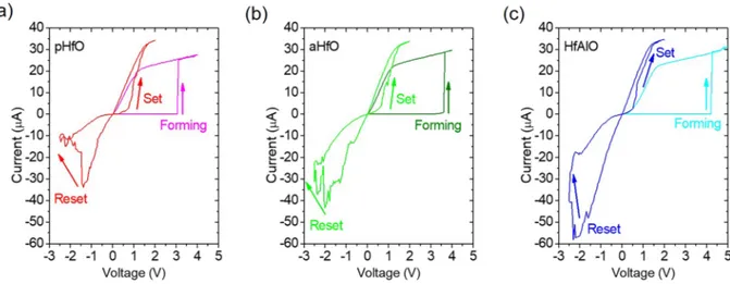
Figure 3shows the measured quasistatic I-V curves of (a) p-HfO, (b) a-p-HfO, and (c) HfAlO RRAM devices. The characteristics include the forming operation, the first reset transition after form-ing, and the first set transition after the first reset. The experiments were carried out on individual 1T1R devices with the array by using a Keithley 4200-SCS semiconductor parameter analyzer operated within a Cascade PA200 semiautomatic probe station. A voltage from 0 to 5 V was applied to the top electrode during the forming operation with a fixed gate voltage of 1.5 V, corresponding to an IC of about 30 μA at the maximum top electrode voltage. During the reset process, the voltage at the source terminal was increased from 0 to 2.5 V with a gate voltage of 2.8 V, which was large enough to minimize the transistor resistance with respect to the LRS resistance. Finally, during the set procedure, the voltage at the top electrode was increased from 0 to 2 V with a gate voltage of 1.6 V, corre-sponding to an IC around 35 μA at the maximum applied voltage. A sweep rate of 1 V/s was used for all the quasistatic operations inFig. 3.
The I-V curves show typical RRAM behaviors inFig. 3, such as the abrupt forming step at about 4 V, the noisy reset transition, and the low-voltage set process. The latter is particularly beneficial
FIG. 3. Measured quasistatic I-V curves for (a) p-HfO, (b) a-HfO, and (c) HfAlO. The I-V curves show similar behaviors, with abrupt forming, noisy reset transition, and low
set voltage. The latter is particularly beneficial for fine control of the LRS conductance by varying IC.
for proper control of the LRS resistance in analog synaptic applica-tion. In fact, a large set voltage might lead to an unwanted overshoot which results in a poor control of the LRS resistance.27Low set volt-age is therefore an essential property to enable tight control of the LRS conductance and synaptic update in training algorithms such as the backpropagation technique.14
To statistically evaluate the switching behavior of the three RRAM technologies, a pulse mode scheme was applied on 100 1T1R devices integrated in 4 kbit test vehicles by using a pulse width of 10 μs.Figure 4shows (a) the cumulative distribution of the measured forming voltage, (b) first reset voltage, and (c) first set voltage for the various HfO2devices. The forming voltage is defined as the voltage for which the read current measured at Vread= 0.2 V exceeds 18 μA after the applied pulse, where the voltage was incrementally updated by 0.1 V at every attempt, starting from 0.2 V. The set voltage was defined in a similar way, except that set transition was applied after
forming and reset. The reset voltage was defined as the first voltage causing the read current to drop below the verify level of 5 μA.
The results inFig. 4show that p-HfO displays the lowest form-ing voltage compared to other technologies; however, the set and reset voltages show larger values and relatively large spread with respect to a-HfO and HfAlO. Such a large device-to-device variabil-ity in p-HfO devices prevents an accurate analog programming of the RRAM elements for inference application.
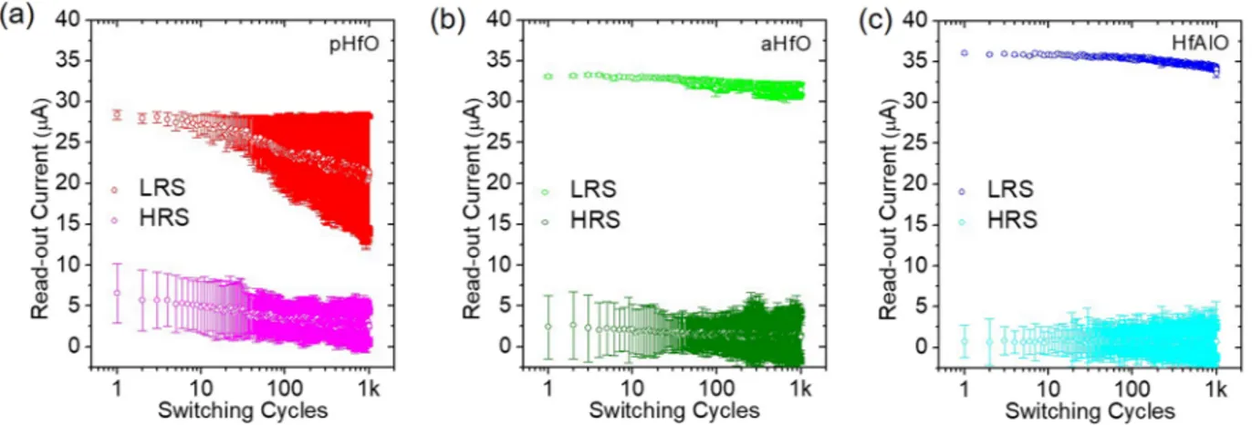
Another crucial property of the RRAM devices is the endurance performance, which was assessed for 1000 consecutive reset/set cycles by using a reset pulse amplitude of 1.8 V and a set pulse amplitude of 1.2 V. The resistance ratio of the RRAM elements was evaluated at Vread= 0.2 V.Figure 5shows the average read current at Vreadas a function of the number of cycles for (a) p-HfO, (b) a-HfO, and (c) HfAlO RRAM. The cell-to-cell variability is shown by using the dispersion coefficient, defined as σ/μ. Both LRS and HRS current
FIG. 4. Cumulative distributions of (a) forming voltage, (b) reset voltage, and (c) set voltage for the three RRAM technology splits, namely, p-HfO, a-HfO, and HfAlO. Although
showing a smaller forming voltage, p-HfO RRAM has higher set/reset voltages and their respective variability. On the other hand, a-HfO and/or HfAlO RRAM structures thus seem best suited for neuromorphic synapse applications.
FIG. 5. Read current as a function of the number of cycles for (a) p-HfO, (b) a-HfO, and (c) HfAlO. The error bar refers to the device-to-device variation for 1000 cells. Note
the larger resistance window and smaller degradation of the LRS current for HfAlO.
decrease with the number of cycles for p-HfO devices, which also leads to a drop of the resistance ratio, mainly caused by the increase in the LRS variability with increasing number of cycles. The degra-dation of the LRS conductance and the higher cell-to-cell variability in the array might be attributed to the grain boundaries conduc-tion mechanism in the p-HfO structure.28 For instance, thermally activated diffusion of the defects from the grain boundary might lead to the gradual loss of conductance inFig. 5(a). On the other hand, a-HfO shows a smaller variability, a larger resistance ratio, and a smaller degradation of the LRS conductance. Finally, the dop-ing by Al atoms in the HfO2layer supports the endurance properties with minimum LRS drop and small variability. These results sug-gest that Al doping stabilizes the HfO2matrix by hindering oxygen-vacancies relaxation without severe changes of the switching param-eters.28The LRS variability in HfAlO is almost suppressed compared with p-HfO and a-HfO, providing an approximately constant resis-tance ratio of about 10. Due to the large resisresis-tance ratio, robust
cycling, and limited variability, HfAlO seems a promising material for RRAM-based neuromorphic synapses.
Figure 6shows a systematic study of the variability for (a) p-HfO, (b) a-p-HfO, and (c) HfAlO RRAM. In the figure, the standard deviation σ for cycle-to-cycle (C2C) and device-to-device (D2D) distributions is shown for both LRS and HRS as a function of the median device resistance μ. Variability data were collected for a sub-set of 1000 1T1R devices integrated in the 4 kbit test vehicle and for 1000 cycles. The steep increase in variability from LRS to HRS can be understood by the contributions of Poisson variation of the defect number29,30and the shape variation of the filamentary path within HfAlO.31Although the spread σ shows a similar behavior for all three RRAM technologies, HfAlO exhibits the largest resistance ratio between the LRS and HRS regions, in line with the results of Fig. 5. Also, note that HfAlO displays a better endurance compared with p-HfO and a-HfO counterparts since, based on the variability characteristics shown inFig. 6, it is easier to control the conductance
FIG. 6. Standard deviation σ of the resistance as a function of the median resistance R for (a) p-HfO, (b) a-HfO, and (c) HfAlO. Despite the similar trend of σ, HfAlO displays
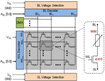
FIG. 7. Schematics of the 4 kbit RRAM array used to demonstrate an inference
machine in hardware. It includes 64 × 64 cells with the 1T1R structure based on an HfAlO RRAM device serially connected to a select NMOS transistor.
for HfAlO devices, which is in addition to the fact that its resistance window is larger. As reported in Ref.28, once a desired conduc-tance level is achieved, HfAlO devices show less instability during cycling. These results confirm the lower variability and large window induced by Al doping and amorphous structure. In the following, this RRAM technology will be considered for the implementation of artificial synapses in inference machines.
IV. MULTILEVEL PROGRAMMING OF HfAlO RRAM DEVICES
To explore the ability to store analog weights in RRAM synapses, we selected HfAlO RRAM as the best technology from
the previous study, thanks to the improved resistance window, yield, endurance, and variability. The multilevel storage in HfAlO RRAM devices was studied for a 4 kbit array with 1T1R structures, which is schematically shown inFig. 7. In addition to the memory and select transistor elements, the array also comprises (i) bit line (BL) and word line (WL) address decoders to access the single 1T1R cells, (ii) the BL voltage selection block and source line (SL) voltage selection block that provide the voltages to activate forming/set/reset opera-tions into RRAM devices, and (iii) a direct memory access (DMA) interface connected with the BL decoder that provides the readout current to selected devices.32
The key point making HfAlO RRAM suitable for neuromor-phic applications is its ability to store multiple resistive states thanks to its limited resistance variability. In particular, HfAlO RRAM enables to program up to 5 resistance states to implement synap-tic weights of the neural network. The first level, which is called L1, corresponds to the HRS and was achieved by a programming scheme under incremental step pulse with verify algorithm (ISPVA) approach consisting of the application of sequential reset pulses with increasing amplitude from 0 to 3 V at source terminal of cell selectors with grounded drain, gate terminal biased at 2.7 V, and a threshold current Ith = 5 μA [Fig. 8(a)]. On the other hand, the other 4 programmable levels correspond to different LRS (L2-L5) and were achieved via a multilevel application of ISPVA strategy (M-ISPVA) schematically described inFig. 8(b). Here, a sequence of voltage pulses with increasing amplitude from 0 to 3 V is applied to the drain of the transistor with grounded source and gate biased by a variable voltage VGin the range 1 V–1.6 V to obtain increas-ing IC and thus decreasing LRS.24In addition, whereas a thresh-old current of 5 μA was set for L1, current targets of 15 μA, 30 μA, 45 μA, and 60 μA were used in the M-ISPVA program-ming scheme to achieve L2, L3, L4, and L5 levels, respectively. Note that each sequential voltage pulse applied to source/drain to achieve HRS/LRS is followed by a read pulse to check that the cur-rent target set for each level is reached. To test the efficiency of the M-ISPVA approach, resistance levels in HfAlO RRAM were
FIG. 8. Schematic representation of (a) the ISPVA approach used to program L1, which is the HRS, and (b) multilevel ISPVA (M-ISPVA) approach to program the other
4 levels (L2-L5) corresponding to LRS with decreasing resistance achieved by application of increasing VGor compliance currents IC. (c) Normalized resistance spread
cells [Fig. 8(c)] evidencing a similar behavior with slope close to 1 of the relative variability of resistance for increasing average resistance.31
Note that the ISPVA and M-ISPVA techniques do not specif-ically require linearity and symmetry of weight update, which are instead key requirements for backpropagation techniques of on-line training.11,14For off-line training, the essential feature of memory
devices is the ability to store multilevel weights which can be pro-grammed at time zero as a code to perform pattern recognition during the system lifetime. This is the main criterion for selecting the most suitable memory device as the synaptic element in the neural network.
V. NEURAL NETWORK FOR INFERENCE DEMONSTRATION
As shown inFig. 9(a), the 2-layer neural network designed into the 4 kbit RRAM array consists of 197 input neurons, 20 hidden neurons, and 10 output neurons. The network was first trained in simulation on the well-known MNIST dataset of handwritten dig-its by a supervised learning approach based on the backpropagation rule.12According to this scheme, the signal emitted by input neu-rons in response to image submission is forward propagated through all network layers leading to generation of an error signal which is calculated as a difference of effective output signal and expected network response. Sequentially, the error signal calculated at the out-put stage is backpropagated toward the inout-put layer and exploited to
image presentations. After repeating this training scheme (forward and backward cycles) with a learning rate parameter of 0.01 for 20 epochs, where each epoch consists of the presentation of the entire training dataset based on 60 000 images, the final weight matrix was used to test the ability of the simulated network to correctly classify 10 000 unseen MNIST images resulting in an inference accuracy of 92%. Note that the array size forced us to use a downscaled version (14 × 14 pixels) of original 28 × 28 MNIST images for both training and inference phases.
To achieve in hardware an inference accuracy close to the one obtained in simulation by using only 5 resistance levels, we applied a random rounding strategy to lower precision of the calculated weight matrix from 64-bit floating point to 5 evenly spaced discrete levels centered around 0. This, however, led to a decrease in infer-ence accuracy at the software level from 92% to 86.5%. Also, since the levels can have both positive and negative signs and device con-ductance can only be positive, we implemented any synaptic weight as difference of two conductances Wij = Gij − Gr, where Gris a fixed reference conductance corresponding to the intermediate level [Fig. 9(b)]. These steps enabled to map the calculated weight matrix based on 5 levels into the 4 kbit array achieving an experimental weight matrix based on 5 current levels.
Although software simulations were carried out using 5 evenly spaced numerical levels, programming operation at the device level is affected by variability. It is highlighted by the probability den-sity function (PDF) distributions of the 5 current levels measured at Vread= 0.5 V inFig. 10(a)where their unavoidable broadening due
FIG. 9. (a) Illustration of neural network
implemented into the 4 kbit RRAM array. Note that neurons labeled “0” in the input layer and hidden layer correspond to bias units. (b) Detailed representa-tion of synaptic weights connecting the input layer to hidden layer evidencing that each weight is implemented as the difference of a trainable conductance Gij
and a reference conductance Gr,i. All
hid-den neurons process input currents via a sigmoid activation function providing a voltage output VHthat becomes the input
signal for next synaptic layer.
FIG. 10. PDF distributions of current levels tested at 0.5 V
(a) before and (b) after a 125○C bake experiment which
causes an additional broadening responsible for a signifi-cant overlap among levels.
FIG. 11. (a) Experimental classification accuracy of the network as a function of Vreadfor variable slopes of the sigmoidal neuron transfer function before and after an annealing experiment at T = 125○C. Best inference performance of about 83% at 0.5 V with no temperature annealing is however lower than accuracies achieved in software with
5 ideal levels (86.5%) and using 64 bit floating point precision (92%). An inference performance of 72% is achieved after the annealing experiment. Confusion matrices of experimental inference accuracy (b) before and (c) after 1 h-long temperature annealing process for the 2-layer neural network implemented in the 4 kbit RRAM array.
TABLE II. Comparison of neural networks assembled into memristive arrays to investigate energy efficiency.
Work Device stack N. synapses (k) MNIST image size Gmax(μS) ηtest(%)
Reference14 GST-PCM 165 22 × 24 pixels 20 82.9
Reference15 Ta/HfO2/Pt RRAM 8 8 × 8 pixels (grayscale) 400 91.71
Our work TiN/Ti/HfAlO/TiN RRAM 4 14 × 14 pixels 200 82.82
to variability can lead to some overlap between consecutive levels. To test temperature retention of current levels after programming operation, array cells were subjected to an annealing experiment at temperature T = 125○
C for 1 h. As a result, a level shift toward lower currents combined with an additional broadening of PDFs were observed, which resulted in highly overlapping current levels, as shown inFig. 10(b).
In view of the cell-to-cell variability of resistance inFig. 10, achieving more than 5 levels might be challenging for our HfAlO RRAM. Therefore, we considered only 5-level synapses in our neu-ral network with a consequent limitation in accuracy of recogni-tion. Achieving more than 5 levels would require to finely tune the ISPVA algorithm parameters, such as step voltage and compliance current, at the expense of time and energy of the multilevel pro-gramming. Alternatively, it might be possible to control the cell-to-cell variability by carefully engineering the RRAM materials and stack.
VI. PERFORMANCE OF THE NEURAL NETWORK Inference ability of 2-layer neural network implemented at the array level was evaluated testing the experimental weight matrix in simulation via presentation of MNIST test dataset containing 10 000 binary digit images unused during the learning phase. In our appli-cation, on pixels within presented image indicate the application of a test voltage Vread, which can vary from 0.1 V to 0.5 V, to correspond-ing synaptic device, whereas off pixels correspond to zero voltage application.Figure 11(a)shows inference performance as a function
of Vreadfor variable slope of the neuron activation function. Here, maximum inference accuracy ηtest obtained before performing the temperature annealing is 82.82%, whereas ηtest= 72% was obtained after the experiment, which supports detrimental effect of the bake-induced level broadening on inference capability of the neural net-work. Results also evidence that best accuracy is achieved by using the maximum read voltage Vread= 0.5 V, which reduces the impact of nonlinearity on programmed current levels, and a sigmoid slope of 2 × 10⁴ V/A in both cases. However, note that increasing the read voltage amplitude during the inference phase also leads to an
FIG. 12. Calculated inference for increasing array size using 5 levels with
vari-ability lower than experimental varivari-ability (red dots) and 9 levels (blue dots). Note that the additional levels were obtained in simulation using intermediate resistance between consecutive levels and their corresponding relative variability shown in
FIG. 13. Calculated inference confusion matrix achieved using 9 levels instead of 5 in case of (a) 4 kbit array, (b) 8 kbit array, and (c) 16 kbit array.
increase in power consumption since the power dissipated in each synaptic element is given byP = VreadIread ≈ Vread2 /R. This indi-cates that there is an inherent tradeoff in our synaptic array between inference accuracy and energy efficiency.
Figures 11(b)and11(c)show the confusion matrices captur-ing ability of neural network to associate each digit from 0 to 9 with corresponding class before and after the annealing experiment, respectively. As expected, low performance suggested by the con-fusion matrix inFig. 11(c)further confirms the strongly negative impact of annealing on classification of almost all digits compared with recognition accuracy exhibited by network inFig. 11(b).
While inference accuracy achieved on MNIST test dataset by our array is still far from software performance, our implementa-tion is competitive with other recently proposed hardware neural networks, especially in terms of energy consumption during the inference phase. To get an estimation of energy consumed by our 4 kbit neural network during inference cycles, we considered (i) the number of operations involved into matrix-vector multiplications at each network layer given by the array size of 4 kbit, (ii) the width of applied read pulses or cycle duration tp = 12 μs, and (iii) the calculated power dissipated on average per inference cycle at Vread = 0.5 V, which is P ≈ 20 mW, eventually achieving a power effi-ciency of about 17 GigaOps/s/W. However, note that tp could be lowered to 10 ns by improvements of array and measurement setup, thus enabling to reach a power efficiency of about 20 TeraOps/s/W, which is four orders of magnitude better than state-of-art CPUs and GPUs.33
Also, while a detailed comparison with other small/medium-scale hardware networks is quite difficult, a good estimate can how-ever be obtained taking into account fundamental parameters such as the number of synaptic devices, the maximum synaptic con-ductance Gmax, and the behavior of conductance response. As first benchmark, a classification accuracy of 82.9% was experimentally demonstrated in Ref.14using a 1T1R PCM array with 165 000 2-PCM synapses featured by Gmax= 20 μS. Compared to our imple-mentation achieving a similar accuracy, this inference performance obtained in Ref.14however required a number of hardware synap-tic devices (165 000 syn × 2 PCM/syn) being about 80 times the number of devices within our 4 kbit array which results in a lower energy efficiency. More recently, another hardware neural network
including about 8000 synaptic devices was proposed in Ref.15by achieving a higher classification accuracy of 91.71% in MNIST clas-sification task. Here, key role for achieving such inference accuracy was first played by high linearity of G-response and high maximum conductance of Ta/HfO2/Pt RRAM synaptic devices Gmax= 400 μS, which is at least twice Gmax in our implementation (seeTable II). These considerations combined with higher synaptic density and application of variable voltage at the input layer to encode MNIST grayscale images lead to high power consumption to reach high per-formance. Unlike aforementioned studies, our 4 kbit array is able to realize an inference machine capable of combining a good inference accuracy with low-power operation thanks to the novel M-ISPVA approach whose refinement via material engineering promises a more accurate control of device variability and consequently higher power and classification efficiency.
In this frame, to evaluate the potential of an improved M-ISPVA approach, we calculated inference ability for HfAlO RRAM arrays of size 4 kbit, 8 kbit, and 16 kbit. As shown inFig. 12, decreas-ing level variability leads to a higher inference accuracy increasdecreas-ing for larger arrays (red dots). Additionally, the use of more levels (9 levels in this case) allows us to improve network inference ability further, enabling to achieve classification accuracies higher than 90% for arrays of size larger than 4 kbit (blue dots). Finally, to support the calculated results obtained using 9 levels for synaptic weights, Fig. 13shows the corresponding inference confusion matrices which evidence a significant improvement in terms of network ability to classify all the digits compared to experimental results shown in Fig. 11(b).
VII. CONCLUSIONS
This work investigates the RRAM-based synaptic devices for neural networks with improved tradeoff between energy efficiency and classification accuracy. We show that RRAM devices with amor-phous HfAlO have superior performance with respect to p-HfO and a-HfO in terms of resistance window, variability, and endurance. 5-level synaptic weights are stored in a 4 kbit array with the 1T1R structure by using a novel multilevel programming scheme. An inference accuracy larger than 80% is demonstrated in a 2-layer neu-ral network with limited operation current thanks to relatively high
resistance of the analog LRS synapses. Statistical cell-to-cell vari-ability limits the maximum number of levels because of the over-lap between adjacent resistance distributions, hence the maximum accuracy of recognition. Our work shows that the combination of material engineering and algorithm-based weight programming can enable inference machines with scalable circuit area, low-power con-sumption, and good recognition accuracy which are required for AI tasks in the edge.
ACKNOWLEDGMENTS
This article has received funding from the European Research Council (ERC) under the European Union’s Horizon 2020 research and innovation programme (Grant Agreement No. 648635), from the Università degli Studi di Ferrara under the Bando per il finanzia-mento della ricerca scientifica “Fondo per l’Incentivazione alla Ricerca” (FIR) – 2018, and from the German Research Foundation (DFG) in the frame of the research group Grant No. FOR2093. REFERENCES
1
Y. LeCun, Y. Bengio, and G. Hinton,Nature521, 436–444 (2015). 2
A. Coates, B. Huval, T. Wang, D. J. Wu, A. Y. Ng, and B. Catanzaro, in Pro-ceedings of the 30th International Conference on Machine Learning (PMLR, 2013), Vol. 28, No. 3, pp. 1337–1345.
3
N. P. Jouppiet al., in Proceedings of the 44th Annual International Symposium on Computer Architecture (ISCA) (IEEE, 2017), pp. 1–12.
4K. He, X. Zhang, S. Ren, and J. Sun, inIEEE International Conference on Computer Vision (ICCV) (IEEE, 2015), pp. 1026–1034.
5
D. Silveret al.,Nature529, 484–489 (2016). 6
H.-S. P. Wong and S. Salahuddin,Nat. Nanotechnol.10(3), 191–194 (2015). 7
D. Ielmini and H.-S. P. Wong,Nat. Electron.1, 333–343 (2018). 8
S. Yu, Y. Wu, and H.-S. P. Wong,Appl. Phys. Lett.98, 103514 (2011). 9
A. Prakash, J. Park, J. Song, J. Woo, E.-J. Cha, and H. Hwang,IEEE Electron Device Lett.36(1), 32–34 (2015).
10A. Athmanathan, M. Stanisavljevic, N. Papandreou, H. Pozidis, and E. Eleftheriou,IEEE J. Emerging Sel. Top. Circuits Syst.6(1), 87–100 (2016). 11
S. Yu,Proc. IEEE106(2), 260–285 (2018).
12
Y. LeCun, L. Bottou, Y. Bengio, and P. Haffner,Proc. IEEE86(11), 2278–2324 (1998).
13M. Prezioso, F. Merrikh-Bayat, B. D. Hoskins, G. C. Adam, K. K. Likharev, and D. B. Strukov,Nature521(7550), 61–64 (2015).
14
G. W. Burret al., in IEEE IEDM Technical Digest (IEEE, 2014), pp. 697–700. 15
C. Liet al.,Nat. Commun.9, 2385 (2018). 16
P. Yao, H. Wu, B. Gao, S. B. Eryilmaz, X. Huang, W. Zhang, Q. Zhang, N. Deng, L. Shi, H.-S. P. Wong, and H. Qian,Nat. Commun.8, 15199 (2017).
17M. Bocquet, T. Hirztlin, J.-O. Klein, E. Nowak, E. Vianello, J.-M. Portal, and D. Querlioz, inIEEE IEDM Technical Digest (IEEE, 2018), pp. 484–487. 18
Z. Zhouet al., in IEEE IEDM Technical Digest (IEEE, 2018), pp. 488–491. 19
E. Ambrosi, A. Bricalli, M. Laudato, and D. Ielmini,Faraday Discuss.213, 87–98 (2019).
20K. Morgan, R. Huang, S. Pearce, and C. de Groot, inIEEE International Symposium on Circuits and Systems (ISCAS) (IEEE, 2014), pp. 432–435. 21
A. Grossiet al.,Sci. Rep.8, 11160 (2018). 22
M. Lanza, K. Zhang, M. Porti, M. Nafría, Z. Y. Shen, L. F. Liu, J. F. Kang, D. Gilmer, and G. Bersuker,Appl. Phys. Lett.100, 123508 (2012).
23G. Bersukeret al.,J. Appl. Phys.
110, 124518 (2011). 24D. Ielmini,IEEE Trans. Electron Devices
58(12), 4309–4317 (2011).
25H. Y. Lee, P. S. Chen, T. Y. Wu, Y. S. Chen, C. C. Wang, P. J. Tzeng, C. H. Lin, F. Chen, C. H. Lien, and M.-J. Tsai, inIEEE IEDM Technical Digest (IEEE, 2008), pp. 297–300.
26Y. Y. Chen, L. Goux, S. Clima, B. Govoreanu, R. Degraeve, G. S. Kar, A. Fantini, G. Groeseneken, D. J. Wouters, and M. Jurczak,IEEE Trans. Electron Devices 60(3), 1114–1121 (2013).
27S. Ambrogio, V. Milo, Z. Wang, S. Balatti, and D. Ielmini,IEEE Electron Device Lett.37(10), 1268–1271 (2016).
28
E. Pérez, A. Grossi, C. Zambelli, P. Olivo, R. Roelofs, and Ch. Wenger,IEEE Electron Device Lett.38(2), 175–178 (2017).
29S. Balatti, S. Ambrogio, D. C. Gilmer, and D. Ielmini,IEEE Electron Device Lett. 34(7), 861–863 (2013).
30
S. Ambrogio, S. Balatti, A. Cubeta, A. Calderoni, N. Ramaswamy, and D. Ielmini,IEEE Trans. Electron Devices61(8), 2912–2919 (2014).
31D. Ielmini,Semicond. Sci. Technol.
31, 063002 (2016).
32C. Zambelli, A. Grossi, P. Olivo, D. Walczyk, T. Bertaud, B. Tillack, T. Schroeder, V. Stikanov, and C. Walczyk, inIEEE International Conference on Microelectronic Test Structures (ICMTS) (IEEE, 2014), pp. 27–31.
33T. Gokmen and Y. Vlasov,Front. Neurosci.