High-quality diamond grown by chemical-vapor deposition: Improved
collection efficiency in
␣
-particle detection
Marco Marinelli, E. Milani,a)A. Paoletti, A. Tucciarone, and G. Verona Rinati
INFM–Dipartimento di Scienze e Tecnologie Fisiche ed Energetiche, Universita` di Roma ‘‘Tor Vergata,’’ I-00133 Roma, Italy
M. Angelone and M. Pillon
Associazione EURATOM–ENEA sulla Fusione, I-00044 Frascati, Roma, Italy 共Received 2 March 1999; accepted for publication 14 September 1999兲
Diamond films were grown on silicon by microwave chemical-vapor deposition using a CH4– H2
gas mixture. The crystalline quality of the films was assessed through their ␣-particle detection performance, a property highly sensitive to film quality, by using a 5.5 MeV 241Am source. A maximum collection efficiency of 70%, 50% being the average value, was obtained in a 115-m-thick sample after-particle irradiation共‘‘priming effect’’兲. Unprimed efficiency⫽50% maximum, 30% average, was also obtained on other samples. The dependence of the efficiency and the resolving power on the external electric field was studied as well. The results are interpreted by means of a Monte Carlo analysis of the␣-particle detection process. It is concluded that, in the priming process, a saturation occurs of deep defects limiting the as-grown detector performance, and charge collection distance is only limited by grain boundaries located close to the substrate side. Therefore, there is indication that further improvement can be reasonably obtained by increasing film thickness. © 1999 American Institute of Physics.关S0003-6951共99兲02846-6兴
Synthetic diamond films grown by chemical-vapor depo-sition 共CVD兲 have a great potential for applications in sev-eral fields, due to the many共mechanical, optical, electronic, etc.兲 exceptional properties of diamond.1,2 However, their polycrystalline nature and the relatively high concentration of structural defects still represent a severe limitation for many applications. This is why the performance of several diamond-based devices currently under investigation3–5 is strongly influenced by the growth and operating conditions.
A particularly important and high-quality demanding ap-plication of diamond films is nuclear particle detection.6,7 The high-energy gap of diamond results in a very low num-ber of free carriers, leading to extremely low-leakage cur-rents. Moreover, the radiation hardness and the high-temperature operation capability of such devices is strongly increased with respect to silicon-based detectors, a crucial feature in view of the operation of next-generation particle accelerators.8
The main parameters assessing the quality of CVD dia-mond films to be used as particle detectors are the charge collection distance共CCD兲 and the efficiency, defined as fol-lows. When an electron–hole pair is created by an ionizing particle in a parallel-plate detector of thickness 共i.e., elec-trode spacing兲 L, it induces9,10in the external circuit a charge
qc⫽ex/L, x being the total distance the electron and hole
move apart. The CCD is the average drift distance and is given by
␦⫽共e⫹h兲E, 共1兲
where e, h are the electron and hole mobilities,
respec-tively, is the mobility weighted lifetime of electrons and
holes, and E is the applied electric field. The efficiency is the ratio of the collected charge Qc to the total charge Q0
gen-erated by the ionizing particle
⫽Qc/Q0. 共2兲
The link between and ␦ can be deduced from the Hecht theory:11 ⫽␦ L
冋
1⫺ ␦ 4G共1⫺e ⫺2G/␦兲共1⫹e2(G⫺L)/␦兲册
, 共3兲 G being the penetration depth in L of the particles to bedetected关for Eq. 共3兲 we assumede⫽h in Eq. 1 and
uni-form generation of charge over G兴. The lifetime, and there-fore␦ and, are limited by the presence of trapping defects 共impurities and/or grain boundaries兲, so that the collection efficiency is strongly correlated with crystal quality.
In CVD diamond particle detectors a crucial role is played by their thickness. Due to the columnar nature of CVD diamond growth, the crystal quality is much worse close to the substrate interface than at the growth surface. In particular, the CCD has been found to increase with film thickness.12,13 CCDs up to about 250 m have been reported14 in millimeter-thick synthetic diamond after
re-moving about half of the sample thickness from the
poor-quality substrate side. This result was obtained for 90Sr 
particles and in the so-called ‘‘primed’’ state of the detectors 共i.e., an improved response condition obtained by-particle priming irradiation to fill traps兲. Nevertheless, it should be pointed out that this very high CCD corresponds to a charge collection efficiency⬵20% only and is, furthermore, much
lower than the film thickness L, thus indicating a relatively
limited extension in depth of the defect-free surface layer. Similarly, 241Am␣-particle spectra of CVD diamond detec-tors also showed relatively low values of.15
a兲Electronic mail: [email protected]
APPLIED PHYSICS LETTERS VOLUME 75, NUMBER 20 15 NOVEMBER 1999
3216
0003-6951/99/75(20)/3216/3/$15.00 © 1999 American Institute of Physics
In this letter, we report on high-quality CVD diamond films and their application as particle detectors with approxi-mately 70% maximum collection efficiency and average value
具
典
⬵50%: the corresponding CCD values go beyond the film thickness共about 250 and 120m, respectively, in an 115-m-thick sample兲 and are obtained without any removal of diamond from the substrate side. 共Note that, by assump-tion, electron and hole mean-free paths are 1/2 the CCD values.兲 The dependence of the collection efficiency and of the resolving power on the external electric field was also studied. In addition, evidence is presented from Monte Carlo simulations strongly supporting some current assumptions on the priming mechanism.CVD diamond films were deposited in a microwave tu-bular reactor on silicon substrates.16,17 A 1% CH4– H2 gas
mixture was used during the deposition process, while the substrate temperature was fixed at Ts⫽750 °C. A 0.7m/h growth rate was estimated through a cross-section scanning electron microscope image of the films. Careful optimization of both the reactor geometry and the plasma energy density was necessary before the achievement of the best results.
Diamond-based detector prototypes were then built from the above samples. As the top electrode, a circular Au con-tact about 7 mm2 size and 100 nm thick was thermally evaporated on the sample growth surface, while Ag paste was used as the silicon backing contact. The detector re-sponse to 5.5 MeV␣ particles was studied by using a241Am
source. The irradiation was carried out through a pinhole, in the direction normal to the sample surface. The detector out-put was connected through a charge preamplifier and a shap-ing amplifier with a 2 s shaping time to a multichannel analyzer.
It is well known14that CVD diamond detectors must be preirradiated with ionizing radiation共e.g., particles兲 in or-der to achieve the highest detection efficiencies. This prim-ing effect is qualitatively explained through a neutralization of trapping defects by irradiation. Before measuring effi-ciency with ␣ particles, we therefore, irradiated our films with90Sr particles for 60 h.
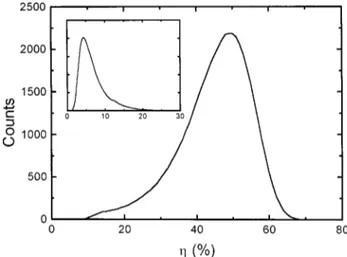
Figure 1 shows the␣-particle detection efficiency of our sample in the primed state for an applied electric field E
⫽40 kV/cm. The horizontal scale, i.e., the Q0 value in Eq. 共2兲, is obtained through calibration with a 100% efficiency silicon detector. It can be seen that the response extends up to a maximum efficiency of about 70%, with a very high-average value of about 50%. It must be stressed that the thickness of our sample is relatively low共115 m兲 and that the whole sample has been utilized, without removing the lower-quality layer close to the substrate. The results, there-fore, indicate that efficiencies very close to 100% might be achieved in CVD diamond detectors with a careful control of the deposition process, thus strongly reducing the perfor-mance gap with silicon-based devices. The reported maxi-mum and average efficiencies correspond 关Eq. 共3兲兴 to ␦ ⬵250m and␦⬵120m, respectively. In other samples of lower thickness the unprimed efficiency reached ⫽50% maximum, with 30% average value, corresponding to ␦ ⫽27m and␦⫽13m, respectively in a 35-m-thick film. We also checked that all the ␣ particles are actually detected. To this purpose, the 241Am ␣ source used was ab-solutely calibrated and the expected count rate was deter-mined by means of a Monte Carlo calculation of the solid-angle factor for the source-to-detector geometry used. It was found that all the ␣ particles which reach the detector are counted in the peak area.
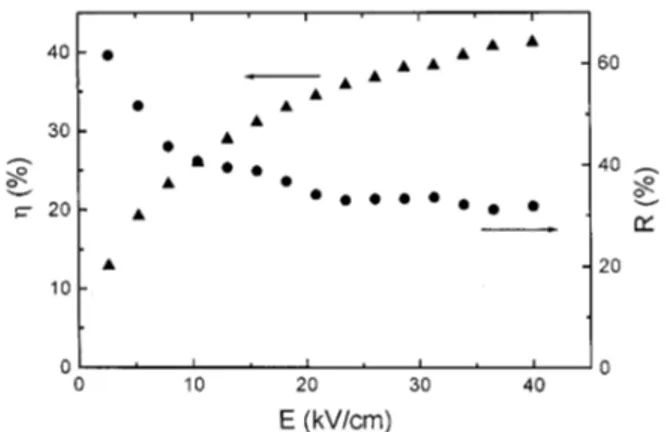
It is well known that the response of particle detectors increases with the applied electric field. However, the in-crease in collection efficiency is accompanied by a widening of the peak, so that higher applied electric fields do not nec-essarily lead to better resolved spectra. In Fig. 2 we report the field dependence of both
具
典
and the ratio R⫽W/具
典
between the full width at half maximum共FWHM兲 W and the mean value具
典
of the response peak, showing that although具
典
is, as expected, monotonically increasing with field, R substantially levels off for fields higher than about 20 kV/ cm.In view of the fundamental importance of the priming effect in the realization of high-efficiency CVD diamond particle detectors, we also tried to get some insight on some current assumptions on the priming mechanism in terms of deactivation of deep traps in the diamond gap. One sees from the␣-particle response curves of our film reported in Fig. 1, in both the primed and unprimed 共inset兲 state, that priming changes not only the position of the peak, but also its shape, from a right-asymmetric 共positive skewness兲 to a
left-FIG. 1.␣-particle response spectra of the detector in the primed共full figure兲 and unprimed共inset兲 state. The collected charge is normalized by the gen-erated charge to give the efficiency.
FIG. 2. Behavior of the mean efficiency共triangles兲 and the resolution R ⫽FWHM/ 共dots兲 of our detector 共in a partially primed state兲 vs applied electric field.
3217
Appl. Phys. Lett., Vol. 75, No. 20, 15 November 1999 Marinelliet al.
asymmetric共negative skewness兲 one. In fact, there are basi-cally two factors limiting the response of CVD diamond par-ticle detectors; namely, in-grain defects and grain boundaries, the latter being not randomly distributed but strongly increasing in concentration towards the substrate side of the sample due to the columnar nature of CVD dia-mond growth. Only the former ones are expected to be de-activated by priming. This picture is strongly supported by a Monte Carlo simulation we developed for CVD diamond
␣-particle detection. We simply modeled in-grain defects by a homogeneous distribution of random trapping centers and grain boundaries by a density distribution D(x)⫽A exp 关⫺x/b兴, where x is the distance from the diamond–substrate interface normalized to the thickness of the sample, and A, b are parameters. By using the␣penetration depth in diamond
G⬵15 m, we obtained the simulated response curves shown in Fig. 3, where the unprimed case was obtained by including both in-grain defects and grain boundaries, and the primed case by including only grain boundaries, with the same distribution utilized in the former curve. In particular, the curves in Fig. 3 are obtained using A⫽75m⫺1 and b ⫽0.08, while the average drift length due to in-grain defects 共left curve兲 is about 6m. These values correspond to a very low concentration of grain boundaries except close to the substrate interface, where a highly defective layer exists. This scenario is in agreement with that expected from the columnar growth of CVD diamond for samples with high-crystalline quality. In spite of the obvious crudeness of the model, the resulting curves reproduce very well the ones measured. The negative skewness appears, therefore, to be characteristic of high-crystalline quality samples where in-grain defects are substantially inactivated and in-grain bound-aries limiting the response in the primed state are substan-tially located only close to the diamond–silicon interface, leading to high values of
具
典
. It has to be stressed that, while the unprimed curve can be reproduced using in-grain defects only, the particular asymmetry of the primed curve strictly requires the particular shape of the grain-boundary distribu-tion.Because our films are almost free of grain boundaries for most of their thickness, increasing the thickness and remov-ing the highly defective interface layer could reasonably lead to extremely high collection distances.
In conclusion, we have shown that very high-particle detection efficiencies can be reached in high-quality CVD diamond films, the priming effect being essential to improve performance. In-grain defects are not limiting the response of our primed films. The efficiency is only limited by grain boundaries close to the diamond–silicon interface, reaching values compatible with charge carrier mean-free paths close to the surface–interface distance; thus, charge collection dis-tances appear subject to further improvement by increasing film thickness and/or removing the substrate interface layer. These results are supported by Monte Carlo simulations giv-ing quantitative account of the transition observed from posi-tive to negaposi-tive skewness in the response curves during the priming process.
The authors thank Professor M. Cirillo for allowing them to use the contact deposition facilities of his laboratory.
1The Properties of Diamond, edited by J. C. Field 共Academic, London,
1979兲.
2The Physics of Diamond, edited by A. Paoletti and A. Tucciarone共IOS,
Amsterdam, 1997兲.
3H. Kawarada, C. Wild, N. Herres, P. Koidl, Y. Mizuochi, A. Hokazono,
and H. Nagasawa, Appl. Phys. Lett. 72, 1878共1998兲.
4T. Ito, M. Nishimura and A. Hatta, Appl. Phys. Lett. 73, 3739共1998兲. 5
R. D. McKeag, S. S. M. Chan, and R. B. Jackman, Appl. Phys. Lett. 67, 2117共1995兲.
6L. S. Pan, S. Han, D. R. Kania, S. Zhao, K. K. Gan, H. Kagan, R. Kass, R.
Malchow, F. Morrow, W. F. Palmer, C. White, S. K. Kim, F. Sannes, S. Schnetzer, R. Stone, G. B. Thomson, Y. Sugimoto, A. Fry, S. Kanda, S. Olsen, M. Franklin, J. W. Ager III, and P. Pianetta, J. Appl. Phys. 74, 1086共1993兲.
7F. Borchelt et al., Nucl. Instrum. Methods Phys. Res. A 354, 318共1995兲. 8C. Bauer, I. Baumann, C. Colledani, J. Conway, P. Delpierre, F. Djama,
W. Dulinsky, A. Fallou, K. K. Gan, R. S. Gilmore, E. Grigoriev, G. Hallewell, S. Han, T. Hessing, K. Honscheid, J. Hrubec, D. Husson, R. James, H. Kagan, D. Kania, R. Kass, K. T. Kno¨pfle, M. Krammer, T. J. Llewellyn, P. F. Manfredi, D. Meier, L. S. Pan, H. Pernegger, M. Per-nicka, V. Re, S. Roe, D. Roff, A. Rudge, M. Schaeffer, M. Schieber, S. Schnetzer, S. Somalwar, V. Speziali, R. Stone, R. J. Tapper, R. Tesarek, W. Trischuk, R. Turchetta, G. B. Thomson, R. Wagner, P. Weilhammer, C. White, H. Ziock, and M. Zoeller, Nucl. Instrum. Methods Phys. Res. A
383, 64共1996兲.
9W. Shockley, J. Appl. Phys. 9, 635共1938兲. 10
S. Ramo, Proc. IRE 27, 584共1939兲.
11K. Hecht, Z. Phys. 77, 235共1932兲.
12M. A. Plano, S. Zhao, C. F. Gardinier, M. I. Landstrass, D. R Kania, H.
Kagan, K. K. Gan, R. Kass, L. S. Pan, S. Han, S. Schnetzer, and R. Stone, Appl. Phys. Lett. 64, 193共1994兲.
13
S. Zhao, Ph.D. dissertation, Ohio State University共1994兲.
14W. Adam, C. Bauer, E. Bedermann, F. Bogani, E. Borchi, M. Bruzzi, C.
Colledani, J. Conway, W. Dabrowsky, P. Delpierre, A. Daneuville, W. Dulinsky, B. van Eijk, A Fallou, D. Fish, F. Foulon, M. Friedl, K. K. Gan, E. Gheeraert, E. Grigoriev, G. Hallewell, R. Hall-Wilton, S. Han, F. Hartjes, J. Hrubec, D. Husson, H. Kagan, D. Kania, J. Kaplon, R. Kass, K. T. Kno¨pfle, M. Krammer, P. F. Manfredi, D. Meier, M. Mishina, F. Le-Normand, L. S. Pan, H. Pernegger, M. Pernicka, S. Pirollo, V. Re, J. L. Riester, S. Roe, D. Roff, A. Rudge, S. Schnetzer, S. Sciortino, V. Speziali, H. Stelzer, R. Stone, R. J. Tapper, R. Tesarek, G. B. Thomson, M. Traw-ick, W. Trischuk, R. Turchetta, A. M. Walsh, R. Wedenig, P. Weilham-mer, H. Ziock, and M. Zoeller, Proceedings of the Electrochemical Soci-ety’s 5th Symposium on Diamond Materials共1998兲, p. 491.
15
E. Bedermann, K. Blasche, P. Moritz, H. Stelzer, and F. Zeytouni, Pro-ceedings of the 36th International Winter Meeting on Nuclear Physics 共1998兲, p. 216.
16G. Balestrino, M. Marinelli, E. Milani, A. Paoletti, I. Pinter, and A.
Tebano, Appl. Phys. Lett. 62, 879共1993兲.
17
M. Marinelli, E. Milani, M. Montuori, A. Paoletti, P. Paroli, and J. Tho-mas, Appl. Phys. Lett. 65, 2839共1994兲.
FIG. 3. Monte Carlo simulation of the␣-particle response curves of our detector in the primed共full figure兲 and unprimed 共inset兲 state.
3218 Appl. Phys. Lett., Vol. 75, No. 20, 15 November 1999 Marinelliet al.