Alma Mater Studiorum · Universit`
a di Bologna
Scuola di Scienze
Corso di Laurea Magistrale in Fisica
Optoelectronic properties of LaVO
3
perovskite for photovoltaic applications
investigated by surface potential
measurements
Relatore:
Prof.ssa Daniela Cavalcoli
Correlatore:
Dott.ssa M. Antonietta Fazio
Presentata da:
Margherita Sola
Sessione I
Optoelectronic properties of LaVO
3
perovskite for photovoltaic applications
investigated by surface potential
measurements
Abstract
La ricerca su materiali innovativi per applicazioni fotovoltaiche si `e orientata negli ulti-mi anni verso lo studio delle perovskiti, utilizzate per lo sviluppo di nuove tipologie di celle solari ad alta efficienza e basso costo. Negli ultimi anni, si `e assistito ad un incre-dibile sviluppo delle celle solari basate sulle perovskiti, che, all’inizio del 2016, hanno raggiunto un’efficienza certificata del 22.1% [1], un valore impressionante considerata la loro scoperta molto recente. Tuttavia, la commercializzazione di tali celle solari `e ancora lontana, a causa della loro grande instabilit`a. L’ossido di lantanio-vanadio (LaVO3) `e
un ossido composto da due metalli di transizione che presenta la struttura cristallina della perovskite. Questo materiale `e molto promettente per applicazioni fotovoltaiche, in quanto potrebbe risolvere il problema della stabilit`a.
Lo scopo di questa tesi `e quello di studiare sperimentalmente questo materiale, e di va-lutarne la possibile applicazione nello sviluppo di dispositivi solari a basso costo e alte prestazioni.
In questo contesto, gli obiettivi della tesi sono stati: lo studio delle propriet`a ottiche ed elettriche del LaVO3, condotto con metodi di surface photovoltage (SPV);
l’implementa-zione e l’ottimizzal’implementa-zione di un apparato sperimentale di surface photovoltage spectroscopy (SPS), insieme con lo sviluppo del relativo software di acquisizione dati.
L’apparato per SPS `e stato implementato con successo, il set-up sperimentale `e stato ottimizzato al fine di migliorare il segnale misurato ed `e stato sviluppato un software per il controllo del sistema e l’acquisizione dati.
Lo studio delle propriet`a morfologiche del LaVO3 alla nanoscala, condotto mediante
mi-croscopia a forza atomica, ha permesso l’identificazione delle condizioni di deposizione ottimali dei film sottili. Lo studio delle propriet`a elettriche alla nanoscala, condotto mediante scanning Kelvin probe microscopy, ha permesso la determinazione del valore dell’altezza barriera all’interfaccia LaVO3/ZnO e delle work function di ZnO e LaVO3.
Si noti che il valore di work function del LaVO3 non era mai stato riportato prima in
letteratura. Le misure SPV sul LaVO3 hanno generato un segnale minore del limite di
rilevazione dell’apparato: ci`o significa che le coppie elettrone-lacuna fotogenerate non vengono separate e raccolte in modo efficiente.
In conclusione, il LaVO3 `e noto per avere propriet`a ottiche ottimali ed elevata stabilit`a,
che sono vantaggi considerevoli per eventuali dispositivi fotovoltaici. Tuttavia, le misure di SPV, che sono sensibili alle propriet`a di trasporto oltre a quelle ottiche, hanno chia-ramente dimostrato che questo materiale non `e ottimale come mezzo per il trasporto di carica. Perci`o, i campioni di LaVO3 analizzati non sono adatti per applicazioni
fotovol-taiche. Per risolvere il problema, la soluzione potrebbe essere quella di incorporare nella struttura materiali per il trasporto dei portatori, creando cos`ı una struttura “mista” [2]. In una simile struttura, le numerose interfacce presenti consentirebbero la separazione e la raccolta delle coppie elettrone-lacuna fotogenerate. Queste considerazioni potrebbero aprire la strada a sviluppi futuri relativi allo studio e all’ottimizzazione del LaVO3 come
materiale per applicazioni fotovoltaiche.
The research on innovative materials for photovoltaic application has recently focused on perovskites for the development of new types of high efficiency and low cost solar cells. Perovskite based solar cells faced indeed an unbelievable increase in the last years, reaching a certified efficiency of 22.1% in early 2016 [1], an impressive value considering their recent discovery. However, perovskite based solar cells are still far from commer-cialization because of their high instability. Lanthanum-vanadium oxide (LaVO3) is a
transition metal oxide perovskite promising for photovoltaic applications, which could overcome the stability issue.
Aim of the present thesis is the experimental study of this material and the evaluation of its possible application in the development of low cost and high performance solar devices.
Within this framework, the objectives of the thesis were: the investigation of LaVO3
optical and electrical properties by surface photovoltage (SPV) studies; the implementa-tion and optimizaimplementa-tion of a surface photovoltage spectroscopy (SPS) experimental set-up, along with the development of the related data acquisition software.
The SPS set-up has been successfully implemented, the experimental set-up has been optimized in order to enhance the measured signal and a software for data acquisition
and system control has been developed. The study of LaVO3 morphological properties
at the nanoscale, by atomic force microscopy, allowed for the identification of the optimal deposition conditions of the layers. The study of the electrical properties at the nanoscale by scanning Kelvin probe microscopy allowed for the determination of the barrier height value at the LaVO3/ZnO interface and the work functions of ZnO and LaVO3. It is
note-worthy that the measured value of the work function of LaVO3 has never been reported
in literature up to now. Surface photovoltage spectroscopy on LaVO3gave a signal below
the detection limit of the apparatus, showing that photogenerated electron-hole pairs are inefficiently separated and thus collected.
In conclusion, LaVO3 is known to have optimal optical properties and high stability,
which are considerable benefits for possible photovoltaic devices. However, SPV mea-surements, which are sensitive to transport properties besides the optical ones, have clearly shown that this material is a poor charge-transport medium. As a consequence, it can be concluded that LaVO3 investigated layers are not suitable for photovoltaic
applications. To overcome this limitation, a solution could be the incorporation of addi-tional carrier-transport materials into a mixed structure [2]. In such a structure, a huge number of internal interfaces between the individual solar absorber and nanostructured charge transport media would enable the separation and collection of photogenerated electron-hole pairs. These considerations could pave the way for future developments on the study and optimization of LaVO3 perovskite as a material for photovoltaic
Contents
Introduction 1
1 Photovoltaics: for a sustainable energy future 3
1.1 Current energy trends . . . 3
1.2 The physics of solar cells . . . 6
1.3 Photovoltaics: basic principles . . . 7
1.3.1 The solar resource . . . 8
1.3.2 Characteristics of the photovoltaic cell . . . 9
1.3.3 Detailed Balance . . . 12
1.3.4 Limiting efficiency: the Shockley-Queisser limit . . . 14
1.3.5 The ideal photoconverter and some problematic issues . . . 16
1.4 Strategies for high efficiencies: emerging photovoltaics . . . 18
1.4.1 CIGS thin film solar cells . . . 20
1.4.2 Multi-junction solar cells . . . 21
1.4.3 Dye-sensitized solar cells and organic photovoltaics . . . 22
1.4.4 The rise of perovskite . . . 23
2 Analysis on materials for photovoltaic applications: surface photovoltage (SPV) 27 2.1 The physics of SPV . . . 28
2.1.1 Electrical properties of semiconductor surfaces . . . 28
2.1.2 The surface photovoltaic effect . . . 31
2.2 Experimental set-up . . . 31
2.2.1 The Kelvin probe . . . 32
2.2.3 Scanning SPV measurements . . . 34
2.3 Applications of SPS . . . 34
2.3.1 Bandgap energy and semiconductor type . . . 35
2.3.2 Defect state characterization . . . 36
2.3.3 Characterization of multilayer structures . . . 36
3 Materials and Methods 39 3.1 LaVO3 . . . 39
3.2 Experimental methods . . . 43
3.2.1 Transmittance and SPS measurements set-up . . . 43
3.2.2 Data acquisition program . . . 50
3.2.3 Atomic Force Microscopy . . . 57
3.2.4 Image processing and analysis . . . 63
4 Results 65 4.1 Experimental set-up optimization . . . 66
4.1.1 QTH and Xe stability test . . . 66
4.1.2 Pyroelectric sensor functionality test . . . 68
4.1.3 Monochromator set-up test . . . 68
4.2 Transmittance measurements . . . 71
4.2.1 System functionality test . . . 71
4.2.2 LaVO3 transmittance measurements . . . 72
4.3 SPV measurements . . . 75
4.3.1 System functionality and working frequency tests . . . 75
4.3.2 LaVO3 SPV measurements . . . 77 4.4 AFM measurements . . . 79 4.4.1 Morphological analysis . . . 79 4.4.2 Electrical characterization . . . 84 Conclusions 87 Acknowledgments 91 Bibliography 92
Introduction
The last decade witnessed an astonishing development in the renewable energies field, considered to be the best alternative to fossil fuels for energy production. Among all the available renewable energy sources, photovoltaics is the most promising one, as solar energy is free and widely distributed over the Earth and it drives to a low release of pollutants. Moreover, in the last years, a rapid decrease in the production costs of Si based solar cells paved the way to a fast diffusion of photovoltaics technology.
In particular, the research is focused on the development of new types of photovoltaic devices, the so called third generation solar cells, whose main features are high efficiency and low cost production. Within this framework, the research of new photovoltaics ma-terials plays a crucial role.
Perovskites have been considered as promising photovoltaic materials for the first time around the year 2000; the first solar cell was obtained in 2012, around 50 papers were published on this subject in 2012, and more than 1000 in 2015 [3]. The tremendous increase in the interest on these materials is due to their optimal properties: strong light absorption, high carrier mobility, compatibility with several materials used in other pho-tovoltaics approaches, and simple approach and low cost of the technology. Perovskite based solar cells faced indeed an unbelievable increase in the last years, reaching a cer-tified efficiency of 22.1% in early 2016 [1], an impressive value considering that seven years ago these devices did not exist at all. However, perovskite PV are still far from commercialization because of their high instability.
In this thesis a peculiar perovskite, lanthanum-vanadium oxide (LaVO3), is investigated.
It is a transition metal oxide (TMO) perovskite, intrinsically much more stable, thus resulting in a considerable benefit for possible photovoltaic devices based on LaVO3.
view of the potential photovoltaic applications.
The main objectives of the present thesis are the following:
1. the implementation and optimization of a surface photovoltage spectroscopy ex-perimental set-up, and the development of the related data acquisition software; 2. the investigation of optoelectronic properties of LaVO3 by surface potential
mea-surements. In particular, surface photovoltage spectroscopy, atomic force mi-croscopy, electrical force and scanning Kelvin probe microscopies have been used to detect the light induced variation of the surface potential and to map surface properties at the nanoscale.
The outline of the thesis is the following. Chapter 1 provides an introduction to current energy trends, namely renewable energy sources among which photovoltaics is on the front line. Then, the working principles of the photovoltaic cell and the state of the art of photovoltaics are described, leading to the perovskite solar cells.
In Chapter 2, the physics of surface photovoltage is described, and the experimental set-ups for surface photovoltage measurements reported in literature are presented. In Chapter 3, after an introduction on LaVO3 material properties, the spectroscopic
set-up implemented in the present thesis is presented in detail. In particular, attention is paid on both its hardware components and its software developed for data acquisition and system control. In the last section, atomic force microscopy and electrical force microscopy techniques employed for morphological and electrical analysis are described. In Chapter 4, the results of all the measurements on different samples are described. A final discussion and some conclusions on the obtained results are presented.
Chapter 1
Photovoltaics: for a sustainable
energy future
1.1
Current energy trends
The world energy system is an enormous and complex machine, and energy transition from fossil fuels to renewable sources is a long and difficult process.
The global primary energy consumption has grown at an average rate of 2.1% per year in the last decade. In 2014 it raised only by 0.9%, reaching an average rate of consumption of 17.2 TW [4]. This increase was the weakest one since 2009, indicating a possible trend towards moderation in the years to come. As shown in Fig. 1.1, fossil fuels yield 87% of the total primary supply, whereas renewable sources are going to reach the 10%. Nuclear has experienced a little increase in the last years, but this is not expected to affect the general trend, that its a progressive reduction, due to the ongoing decommissioning of many reactors in the US and Europe [5]. The demand for fossil energy amounts to 1066 barrels of oil, 108 000 m3 of natural gas and 250 tonnes of coal per second worldwide [4].
Oil still continues to be the first energy source, the largest majority of which (ca. 80%) is used for the transportation system, while the rest is employed for heat and electricity, petrochemicals, asphalt, and lubricants [6].
The predominance of oil products in transportation has lately been weakened by natural gas and electricity, that currently represent 8.5% of the transportation fuels in the US, the largest nonpetroleum share since 1954. After decades of a fairly static scenario, the
Figure 1.1: Global supply of commercialy traded primary energy [4, 6].
world oil system is now undergoing considerable changes, mainly pulled by the depletion of conventional reserves [7].
Natural gas is the most geographically concentrated energy resource; while the largest conventional gas field in the world is between Iran and Qatar, Siberia and the Russian Arctic host three of the top five world deposits. These three countries host nearly 50% of the world’s estimated reserves [4]. In the last decade, the implementation and diffusion of horizontal drilling and hydraulic fracturing in the US has untapped many unconventional gas deposits stuck in shale formations across the country [8]. The US natural gas production has increased by over 40% in the last ten years, bringing the country again as the world’s largest producer, well ahead of Russia [4]. However, these activities have lead to a large environmental and public health discussion, including groundwater contamination, methane release in the atmosphere and induced seismicity. Nevertheless, there is no doubt that natural gas will be increasingly exploited during the first half of this century as a bridge towards renewable energies [9]. The estimated reserves of coal are still the largest among fossil fuels. They could cover the current world demand for over 110 years, compared to 52.5 and 54.1 years for oil and natural gas, respectively [4].
The most relevant change in the world energy landscape in the last years comes from the continuous rise of renewable energies, especially in the electricity field. In 2014, for the first time, global carbon emissions associated with energy production remained
stable despite economic growth. This effect was primarily due to the increasing use of renewables and enhanced energy efficiency [10]. The leading actor in this scenario is China, which now produces as much electricity from sunlight, water and wind as all the power plants in Germany and France combined, covering 20% of its internal demand. In the period 2008-2012, its investments in non-fossil energy plants increased by 40%, whilst those in fossil-fueled facilities were significantly reduced [11].
The exceptional 7-fold drop of the photovoltaics (PV) price in the last decade (mainly caused by a huge increase of the Chinese production) has made PV a truly game changer in the global energy market. The locations where PV electricity is competitive with traditional technologies is continuously increasing and its share of electricity production in many industrialized countries has become remarkable [11]. In 2014, Italy produced about 8% of its energy needs by PV, so far the largest share in the world [6].
Figure 1.2: Global cumulative PV installation over years [12].
All the renewable energy sources are constantly growing. In 2014, hydroelectric global capacity exceeded 1 TW, wind reached 370 GW, and PV almost 180 GW. They re-spectively covered 16.6%, 3.1% and 0.9% of the world electricity demand; although the two last shares seem to be small, they are considerable values, since hydroelectricity has been an established technology for over 120 years, whereas wind and PV were virtually
non-existing just twenty years ago. Furthermore, estimated direct and indirect jobs in renewable energies worldwide are almost 8 million (1.2 million in European Union) and continue to rise [10].
The previous data show that the energy transition from fossil fuels to renewable sources is already ongoing and indicate that PV is at the forefront among renewable energies, as shown by data of last years PV installations presented in Fig. 1.2 [6].
1.2
The physics of solar cells
Sunlight is the most important energy source for humanity: it is homogeneously dis-tributed over the Earth, abundant (90 PW = 90·1015W received on the planet’s surface) and unlimited, since it will last for more than 4 billion years. The current energy con-sumption rate of our civilization (17.2 TW in 2014) is 5000 times smaller than the solar energy irradiating the surface of the Earth [9]. However, mankind cannot use solar en-ergy unless it is converted into a final usable enen-ergy form: heat, electricity, fuels. While conversion of solar energy into heat is direct, its conversion into electricity creates several problems, as explained in the followings.
A solar cell is a device that converts sunlight into electricity through the photovoltaic effect. Photovoltaic energy conversion results from charge generation, charge separation and charge transport.
A photovoltaic solar energy converter absorbs photons to excite electrons to a higher energy level, where they have increased electrochemical potential energy. To make the extraction of the excited electrons possible, an energy gap has to occur in the material band structure: a semiconductor is a very good example of such a system. The separation of the energy bands is needed to maintain the excited electrons at the higher energy for a long time compared to the thermal relaxation time, so that they may be collected. The excited electrons must be extracted and collected: these steps require a mechanism for charge separation. Some intrinsic asymmetry is needed to drive the excited electrons away from their point of creation (Fig. 1.3). In order to complete the photovoltaic conversion process, charges have to be lead to the external circuit; for this reason, the material should be a good electrical conductor. Perfect conduction means that carriers must not recombine with defects or impurities, and should not transfer energy to the
medium. There should be no resistive loss (series resistance) or current leakage (parallel resistance). The material around the junction should be highly conductive and ensure good Ohmic contacts to the external circuit [13].
(a) (b)
Figure 1.3: (a) Band structure of differently-doped semiconductors. (b) Band structure of a p-n junction; principle of photovoltaic device: photon absorption, carrier generation and separation [14].
Charge separation and transport are provided by the semiconductor p-n junction (which is the classical model of a solar cell) as shown in Fig. 1.3 or by another interface with the same electronic features, such as the Schottky barrier or the heterojunction [13].
1.3
Photovoltaics: basic principles
Edmund Bequerel firstly reported the photovoltaic effect in 1839, when he observed the production of an electric current from the action of light on a silver coated platinum electrode immersed in an electrolyte [13].
It was only around the 1950s, with the development of good quality silicon wafers (thanks to the new solid state electronics), that crystalline silicon photovoltaic devices produced potentially useful quantities of power. Chapin, Fuller and Pearson firstly reported in 1954 a silicon solar cell able to convert sunlight with an efficiency of 6% [13].
However, due to their high production cost, estimated about $200 per Watt, these cells were not considered for industrial power generation for several decades.
of secure sources of electricity alternative to fossil fuels.
Although many other materials have been studied, silicon still remains the foremost photovoltaic material, thanks to the advances of silicon technology achieved by the mi-croelectronics industry.
During the late 1990s, the photovoltaic production grew at a yearly rate of 15-25%, driving a relevant reduction in cost and opening up new markets [13].
1.3.1
The solar resource
The Sun emits light with a range of wavelengths, spanning the ultraviolet, visible and infrared sections of the electromagnetic spectrum. Its extra-terrestrial spectrum is similar to that of a black body at 5760 K, although it is considerably attenuated and changed in shape because of the Earth’s atmosphere [13]. This is due to scattering and absorption events by atmosphere particles (oxygen, ozone, and nitrogen, water and CO2), which are
responsible for the dips in the absorption spectrum shown in Fig. 1.4.
Figure 1.4: Extra-terrestrial (AM 0) solar spectrum compared with the standard terres-trial (AM 1.5) solar spectrum. Plot adapted from [15].
Attenuation by the atmosphere is quantified by the Air Mass factor, nAirMass defined as:
nAirMass =
optical path length to Sun
This definition is necessary because, depending on the position of the Sun, rays have to pass through a different width of atmosphere. Because of its great variability, Air Mass 1.5, or AM 1.5, is considered as the standard spectrum, for a total power density content of 1 kW/m2. The AM 1.5 spectrum is an extraterrestrial solar spectrum attenuated by
1.5 thickness of an Earth atmosphere of standard composition [13].
1.3.2
Characteristics of the photovoltaic cell
Open circuit voltage and short circuit current
Charge separation due to incident light establishes a photovoltage when the terminals are isolated (infinite load resistance); this physical quantity is called the open circuit voltage Voc.
The photocurrent drawn when the terminals are connected together is called the short circuit current Isc. For any intermediate load resistance RL, a voltage V between 0
and Voc is established and the cell delivers a current I such that V = IRL, where I(V )
is determined by the current-voltage characteristic of the cell under that illumination. Thus, when a load is connected to the external circuit, the cell produces both current and voltage and it can do electrical work [13].
Photocurrent and quantum efficiency
The size of the current generated by the cell in short circuit depends upon the intensity and the energy spectrum of the incident light. Photocurrent is related to incident spec-trum by the quantum efficiency QE of the cell, which is the probability of generating an electron per incident photon as a function of photon energy. Then the short circuit current density Jsc is:
Jsc= q
Z
bs(E)QE(E)dE (1.2)
where bs(E) is the incident spectral photon flux density (the number of photons of energy
in the range E to E + dE which are incident on unit area in unit time) and q is the electronic charge [13]. QE depends on the absorption coefficient of the solar cell material and on the effectiveness of charge separation and charge collection in the device, whereas
it does not depend on the incident spectrum. For this reason, QE is therefore a key quantity to evaluate solar cell performance under different conditions [13].
Dark current
When a load is present, a potential difference is established between the terminals of the cell, which drives a current in the opposite direction to the photocurrent. This reverse current is usually called the dark current in analogy with the current Idark(V ) which
flows across the device under an applied bias V in the dark. For the p-n junction solar cell, the behaviour is that of a diode in the dark, and for an ideal diode the dark current density Jdark under an applied bias V follows the law:
Jdark(V ) = J0(eqV/kBT− 1) (1.3)
where J0 is a constant, kB is Boltzmann’s constant and T is the temperature [13].
The total current of the cell can be approximated as the sum of the short circuit pho-tocurrent and the dark current. This approximation is reasonable for many photovoltaic materials although the reverse current flowing in response to voltage in an illuminated cell is not formally equal to the current which flows in the dark. The net current density J (V ) in the cell is
J (V ) = Jsc(V ) − Jdark(V ) [13]. (1.4)
As the load resistance is increased, the potential difference increases as a consequence, while the net current decreases, until the photocurrent and dark current exactly cancel out: this is equivalent to the case when the contacts are isolated and the bias has its maximum value, that is the open circuit voltage Voc [13].
Efficiency and fill factor
The working condition of the solar cell is the bias range, from 0 to Voc, in which the
cell delivers power (at V < 0, the illuminated device acts as a photodetector, consuming power to generate a photocurrent; at V > Voc, the device once again consumes power,
operating as a light emitting diode). The cell power density P is:
with J (V ) given by Eq. 1.4. P reaches a maximum at the cell’s maximum power point, called “operating point” [13]. This occurs at some voltage Vm, close to Voc, with
a corresponding current density Jm, shown in Fig. 1.5. The optimum load resistance
corresponds to this point.
The fill factor F F is defined as the ratio:
F F = JmVm JscVoc
(1.6)
and describes the “squareness” of the J − V curve, as shown in Fig. 1.5 [13].
Figure 1.5: The current-voltage (black) and power-voltage (grey) characteristics of an ideal cell. The maximum power density JmVmis given by the area of the inner rectangle.
The outer rectangle has area JscVoc. If the fill factor were equal to 1, the current-voltage
curve would follow the outer rectangle [13].
The efficiency η of the cell is the ratio between the power density delivered at operating point and the incident light power density Ps:
η = JmVm Ps
. (1.7)
These four quantities Jsc, Voc, F F and η are the key performance characteristics of a solar
cell. The performance characteristics values for the most common solar cell materials are listed in Table 1.1. It can be noticed that solar cell materials with higher Jsctend to
Cell Type Area (cm2) Voc (V) Jsc (mA/cm2) F F Efficiency (%) crystalline Si 4.0 0.706 42.2 82.8 24.7 crystalline GaAs 3.9 1.022 28.2 87.1 25.1 poly-Si 1.1 0.654 38.1 79.5 19.8 a-Si 1.0 0.887 19.4 74.1 12.7 CuInGaSe2 1.0 0.669 35.7 77.0 18.4 CdTe 1.1 0.848 25.9 74.5 16.4 Table 1.1: Performance of some PV cells [13].
Parasitic resistances
The solar cell can be modelled as a current generator in parallel with an ideal diode. In real cells, power is dissipated through the resistance of the contacts and through leakage currents around the sides of the device. These effects are electrically equivalent to two parasitic resistances, one in series (Rs) and one in parallel (Rsh) with the cell, as shown
in Fig. 1.6. For an efficient cell, Rs has to be as small and Rsh has to be as large as
possible [13].
Figure 1.6: Equivalent circuit of a real solar cell, with series and shunt resistances [13].
1.3.3
Detailed Balance
The principle of detailed balance gives rise to one of the fundamental physical limitations on the performance of a photovoltaic cell. This relies on the fact that the solar cell exchanges thermal radiation with its surroundings environment: any body which absorbs light must also emit light, because of its finite temperature. The rate of photon emission by the cell must be equal to the rate of photon absorption, so that in the steady-state the concentration of electrons in the material remains constant [13].
In equilibrium
If the cell is in the dark, in thermal equilibrium with the ambient, the current density absorbed from the ambient jabs(E) is:
jabs(E) = q(1 − R(E))a(E)ba(E) (1.8)
where a(E) is the absorbance of the material, i.e. the probability of absorption of a photon of energy E, R(E) is the reflectance, i.e. the probability of photon reflection, and ba is the incident flux of thermal photons from the ambient (it is assumed that each
absorbed photon of energy E generates one electron) [13].
On the other hand, the current density for photon emission jrad(E) is:
jrad(E) = q(1 − R(E))ε(E)ba(E) (1.9)
where ε(E) is the emissivity, i.e. the probability of emission of a photon of energy E. The cell emits these photons by spontaneous emission (or radiative recombination), that is the emission of a photon of the energy released by an excited electron relaxing to its ground state [13].
For preserving a steady state, the current densities jabs (Eq. 1.8) and jrad (Eq. 1.9) must
balance, hence [13]:
ε(E) = a(E). (1.10)
Under illumination
If the cell is under illumination, some electrons are excited, inducing the production of a voltage and a photocurrent; however, in these conditions, spontaneous emission is also increased. This radiative recombination is an unavoidable loss, which means that absorbed solar radiant energy can never be fully utilised by the solar cell.
The delivered current is due to the difference between the flux of photons absorbed from the Sun and the flux of photons emitted by the excited device.
The cell absorbs solar photons of energy E at a rate (1–R(E))a(E)bs(E), where bs is
photon absorption includes a term from thermal photons and therefore:
jabs(E) = q(1 − R(E))a(E) (bs(E) + Cba(E)) (1.11)
where the coefficient of ba is introduced to consider the fraction of the incident ambient
flux which has been replaced by solar radiation [13].
1.3.4
Limiting efficiency: the Shockley-Queisser limit
The power conversion efficiency is the ratio between the incident and the extracted power from the photon fluxes (Eq. 1.7). The incident power density Ps is the integral of the
incident irradiance L(E) (the emitted energy flux density) over photon energy [13]: Ps=
Z
L(E)dE = Z
Ebs(E)dE. (1.12)
For cell power density, Eq. 1.5 is recalled [13]:
P = J (V ) V. (1.13) The power conversion efficiency η is then:
η = J (V ) V Ps
(1.14)
and maximum efficiency is achieved when: d
dV η = d
dV J (V ) V = 0. (1.15) Effect of bandgap
As it has already been said, photocurrent is due to the difference between the flux of photons absorbed from the Sun and the flux of photons emitted by the excited device; then, the photocurrent density at short circuit Jsc can be obtained by integrating over
photon energy [13]:
Jsc = q
Z ∞
0
However, since bands are separated by a bandgap Eg, photons with E < Eg are not
absorbed, because an electron in the lower band needs at least an energy equal to Eg to
be promoted to the upper band. It is assumed that the material is perfectly absorbing and non-reflecting, and that each absorbed photon of energy E ≥ Eg is absorbed to promote
one electron to the upper band. Within these assumptions, the maximum photocurrent is obtained for this specific bandgap. Then:
QE(E) = a(E) = 1 E ≥ Eg 0 E ≤ Eg (1.17) and Jsc= q Z ∞ Eg bs(E)dE [13]. (1.18)
Photocurrent is then only a function of the bandgap and of the incident spectrum. It is clear that the lower is Eg, the greater will be Jsc [13].
On the other hand, voltage is due to the electrochemical potential energy of the excited electron, thus Voc must always be equal to or less than
Eg
q [13].
It is evident that very small or large bandgap values will lead to poor photoconverters: in the first case due to a small working value of V , while in the second due to a small working value of the photocurrent. Hence, considering Eq. 1.15, it is possible to calculate
Figure 1.7: Power spectrum of the Sun modelled as a black body at 5760 K, and power available to the optimum bandgap cell. Clearly, no photons with energy less than Eg
the maximum efficiency. For each spectrum, there is an optimum bandgap at which η has a maximum, and, for a standard solar spectrum, this limit was reported by Shockley and Queisser in 1961: it is around 33% at a bandgap of 1.4 eV, for the standard AM 1.5 solar spectrum [13].
Optimising the performance of the ideal single bandgap photoconverter is therefore a matter of choosing the appropriate material [13].
1.3.5
The ideal photoconverter and some problematic issues
In order to achieve the limiting efficiency, a real device should have strong light absorp-tion, efficient charge separation and charge transport, an optimum energy gap, and an optimised load resistance.
The condition of the bandgap is satisfied by several materials, but the requirement for conductivity makes semiconductors an appropriate choice. Due to their bandgaps in the range 0.5 - 3 eV, semiconductors can absorb visible photons and excite electrons across the bandgap, where they may be collected. The III-V compound semiconductors gallium arsenide (GaAs) and indium phosphide (InP) are favoured for high efficiency cells, having bandgaps close to the optimum (1.42 eV and 1.35 eV, respectively, at 300 K). Silicon is cheap and abundant compared to these III-V materials, and it is the most used solar cell material, despite its less favourable bandgap (1.1 eV). Other compound semiconductors, namely cadmium telluride (CdTe) and copper indium gallium diselenide (CuInGaSe2)
have been developed for thin film photovoltaics. According to recent developments in semiconducting molecular materials, organic semiconductors are promising materials for photovoltaic energy conversion in the future [13].
Besides the intrinsic limit due to the bandgap and the fact that the process is threshold-based, other reasons that limit real solar cells performances are the following.
• Incomplete absorption of the incident light. Photocurrent is reduced since photons are not absorbed when passing through the cell, or being reflected from the front surface or from the contacts.
• Non-radiative recombination of photogenerated carriers. Defect sites trap excited charges, that subsequently recombine before being collected, reducing thus the
photocurrent. This happens where the surface defect density is higher, or near interfaces with another material, or near the junction.
• Voltage drop due to series resistance between the point of photogeneration and the external circuit, that reduces therefore the available power [13].
Other features of materials used for solar energy conversion should be: abundance on the planet, low environmental impact throughout the life cycle, stability for many years under light irradiation, and they should be not too much expensive.
Intermittence and intensity fluctuations due to diurnal cycles and atmospheric condi-tions are other problems concerning solar energy conversion. For this reason, storage components are often required as an integral part of the systems [6].
1.4
Strategies for high efficiencies: emerging
photo-voltaics
Solar cells are classified into three generations, which indicate the order of which each became important.
The first cells are made of crystalline silicon (c-Si), the commercially predominant PV technology. The second generation cells are thin film solar cells, including amorphous silicon, CdTe and CuInGaSe2 (CIGS) cells, and they are quite commercially significant.
The third generation of solar cells includes several thin film technologies, often described as emerging photovoltaics, which are still at research or development stage [13].
Concurrent research progresses into all the three generations, while the first generation technologies are most highly represented in commercial production. c-Si solar cells cur-rently represent about 90% of the market, because of Si is stable, non toxic, abundant and its physical properties are well known. Furthermore, the technology is mature, thanks to the massive use of Si in the microelectronic industry [13].
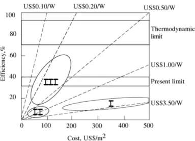
Fig. 1.8 presents the features, in terms of costs and efficiency, of the three generations of cells. The potential benefits of the current research in the third generation solar cells are evident: reaching high efficiency at low cost per power.
Fig. 1.9 shows the state of the art of the highest confirmed efficiencies for different pho-tovoltaic technologies, as reported by National Renewable Energy Laboratory (NREL) [1]. The highest achievements have been obtained so far for multi-junction technologies used in combination with solar concentrators.
In the following paragraphs some of the most promising photovoltaic technologies will be briefly reviewed.
1.4.1
CIGS thin film solar cells
CuIn1−xGaxSe2 (copper indium gallium diselenide, or CIGS) is a direct gap
semiconduc-tor, where the value of x can vary from 0 (CuInSe2, pure copper indium diselenide) to
1 (CuGaSe2, pure copper gallium diselenide). The bandgap varies continuously with x
from about 1.0 eV (for CuInSe2) to about 1.7 eV (for CuGaSe2). CIGS has a chalcopyrite
crystal structure (Fig. 1.10) [17].
Figure 1.10: CIGS unit cell: the lattice elements are tetrahedrally coordinated. Se atoms have two bonds to InGa and two bonds to Cu atoms [17].
CIGS main feature is that it has an optical absorption which is among the highest known for all semiconductors; therefore, a much thinner film is required with respect to other semiconductor materials. Its strong absorption, as well as its availability in both p- and n-types, make it attractive for thin film photovoltaics. The conductivity of p-type CIGS is due to native defects, mostly indium vacancies and copper atoms on indium sites, and can be adjusted by varying the Cu/In ratio during growth. Electron diffusion length is similar to the grain size, determining an internal quantum efficiency up to 90% [13].
1.4.2
Multi-junction solar cells
Single junction solar cells are limited by the material bandgap to a portion of the solar spectrum: photons with energy higher than the bandgap lose their excess energy by ther-malization, while photons with energy below the bandgap are not successfully converted. A possible strategy to increase the efficiency of a solar cell is to stack multiple solar cells using materials with different bandgaps that could exploit a broader range of the solar spectrum, resulting in a multi-junction solar cell, as shown in Fig. 1.11 [18].
(a) (b)
(c)
Figure 1.11: Spectral irradiance vs. wavelength over the AM 1.5 solar spectrum; plots show the parts of the spectrum that can be used, in theory, by: (a) Si solar cells; (b) GaInP/GaInAs/Ge solar cells [18]. (c) Structure of a multi-junction solar cell [19]. Each layer going from the top to the bottom has a smaller bandgap than the previous
one. In this way it absorbs and converts the photons with energies greater than its bandgap and smaller than the bandgap of the higher layer [20].
These solar cells have a maximum theoretical efficiency limit of 86.8% and their main limitation is related to the availability of materials with optimal bandgaps that allow high efficiency due to low defect densities [18].
The best materials for fabricating such multi-junction cells are III-V compound semi-conductors. In fact, they have bandgaps which span a wide spectral range -mostly with direct bandgaps with a high absorption coefficient- and they can also be grown with excellent material quality because of similar lattice constants [18,21]. This is a key fea-ture for the reason why all layers must have similar crystal strucfea-ture, since a mismatch between different layers creates dislocations and significantly deteriorates the efficiency of the solar cell.
The success of this technology has been achieved thanks to these factors, leading to reach the highest solar-to-electric conversion efficiency of any photovoltaic device so far. Clearly, the key problem with multi-junction cells is the high production cost of this technology [18, 21].
1.4.3
Dye-sensitized solar cells and organic photovoltaics
Dye-sensitized solar cells (DSSC) and organic photovoltaics (OPV) will be probably the next PV technology to become commercially significant.
Figure 1.12: Working principle of a dye-sensitized solar cell [6].
linked to a semiconductor electrode and the process is mediated by a redox molecule (R). Therefore, compared to conventional photovoltaics, the DSSC main difference is that light absorption, and electron-hole transport are carried out by different components (dye, semiconductor, electrodes, redox mediator). For this reason, the degrees of freedom to optimize the device are, in principle, many more [6].
Organic photovoltaic (OPV) systems, instead, are based on photoactive p-conjugated polymers and small molecules, as shown in Fig 1.13. The chemical nature of these mate-rials and the simple device architecture often result in lightweight, solution processable and flexible devices. OPV systems are mostly based on abundant elements and low cost materials, can be produced at high manufacturing throughput, and allow easy recycling of constituent materials. These are excellent features for application perspectives and market diffusion [6].
Figure 1.13: Schematic representation of an organic photovoltaic cell with bulk hetero-junction [6].
For several years, expectations for their market debut have been high, but they have materialized only to a very small extent so far. In fact, although DSSC and OPV can be manufactured at smaller economic and energetic cost, they are still not competitive on efficiency and lifetime, which is a strong barrier for a wide market diffusion [6].
1.4.4
The rise of perovskite
Perovskite is a calcium titanium oxide mineral composed of calcium titanate (CaTiO3).
and it is named after Russian mineralogist Lev Perovski [22].
The term perovskite indicates by extension a wide class of compounds that exhibit the same particular crystal structure as CaTiO3 and have the general formula ABX3 (A and
B are two cations of different size and X is an anion that binds to both). A is usually an alkaline earth or rare earth element and B could be a 3d, 4d, and 5d transition metal [6]. Several metallic elements are stable in the perovskite crystal structure, as shown in Fig. 1.14.
Figure 1.14: Perovskite crystal structure [23].
Apart from the structure, perovskites used in PV devices have nothing in common with the rock-solid oxides that naturally occur in minerals. They are synthetic hy-brid organic–inorganic methylammonium lead halide materials of the general formula CH3NH3PbX3 (in which X = I, Br, Cl).
They were firstly used for solar applications by Miyasaka and co-workers in 2009 and by Park and co-workers in 2011. In these works, the hybrid perovskite CH3NH3PbI3 was
used in a DSSC, reporting a cell efficiency of 3.5% in 2009 [24] and 6.5% in 2011 [25]. The sudden rise of perovskite PV begun in 2012, when the two above-mentioned groups published, independently, perovskite-based devices with efficiencies between 9.7 and 10.9%, jointly with the groups of Snaith [26] and Gr¨atzel [27]. In all these works, a solid-state device structure was used, avoiding decomposition of the perovskite absorber in the electrolyte.
Since 2012, several hundreds of papers have been published on this subject, also thanks to the simplicity and low cost of this technology, which can be easily performed with very standard lab equipment. The purpose of these works was to rationalize the working mechanism and to enhance the device efficiency through materials and device
optimiza-tion.
Although the first efficient solid-state perovskite cells were reported only in mid-2012, extremely rapid progress was made during 2013 with energy conversion efficiencies, reach-ing a confirmed 16.2% at the end of the year. This increased to a confirmed efficiency of 17.9% in early 2014 [28], and achieved a certified efficiency of 22.1% in early 2016 [1], an impressive value considering that seven years ago these devices did not exist at all. During these years, the structure of the cell has further evolved, as shown in Fig. 1.15.
(a) (b)
Figure 1.15: Evolution of the architectures of solar cells based on hybrid perovskites. In (a) the perovskite is deposited on mesoporous TiO2 and serves as light absorber and hole
conductor. In (b) the perovskite is deposited as a thin film and serves as light absorber and ambipolar semiconductor, which transports both electrons and holes [6].
The current dominant material in the PV perovskite field remains CH3NH3PbI3, the
best performance described in the seminal paper of Miyasaka and co-workers [24]. This material is cheap, can be easily deposited with wet methods and matches all the following features that, in principle, make it ideal for PV.
• Strong absorption over the entire visible spectral window with the spectral onset at 800 nm (bandgap 1.55 eV), enabling fabrication of very thin films.
• Low “loss-in-potential” within the cell, allowing open circuit voltages (Voc) of over
1.0 V, much higher than DSSC and OPV (0.7–0.8 V).
• A very weak exciton binding energy (0.03 eV), allowing prompt dissociation into free carriers at room temperature.
• High carrier mobility and carrier diffusion lengths as long as 1 µm (i.e. 100 times longer than traditional thin film technologies).
• Ambipolar semiconductor character, enabling an excellent and balanced electron-hole transport, with remarkable simplification of the device.
• An easy crystal-growth control, allowing nearly perfect crystalline films with very low defect densities and ideal charge transport features.
• Compatibility with many materials used in other PV approaches (e.g. DSSC and OPV), which allows testing of new and unconventional device architectures [6]. CH3NH3PbI3 is a material with many positive characteristics, but also relevant problems.
This is the reason why perovskite PV is still far from commercialization. CH3NH3PbI3
can lose its perfect crystallinity at temperatures typically experienced inside solar panels under intensive irradiation and, upon dissolution, it generates PbI2, a carcinogen banned
in many countries.
Perovskite PV experienced a much faster rise of efficiency over time compared to OPV and DSSC. At present, perovskites are envisaged as top cells in future tandem systems to harvest a larger portion of solar spectrum. This would overtake the Shockley and Queisser efficiency limit for single junction systems, which is set at about 31% for per-ovskite cells [6].
Chapter 2
Analysis on materials for
photovoltaic applications: surface
photovoltage (SPV)
The surface photovoltage (SPV) method is a contactless technique for semiconductor characterization that relies on analysing illumination-induced changes in the surface voltage.
This section is intended to provide a brief overview of one specific variant of the SPV method: surface photovoltage spectroscopy (SPS), in which changes in band-bending (both at the free semiconductor surface and at buried interfaces) are monitored as a function of incident photon energy. This technique permits the extraction of many important surface and bulk parameters (bandgap and carriers type, carrier diffusion length and lifetime, surface/bulk state distribution and properties) and can be used for complete construction of surface and interface band diagrams, including the measurement of energy levels in quantum structures.
SPS measurements are contactless and non-destructive; moreover, they can be performed both in situ and ex situ, they are ambient insensitive and capable of any lateral resolution, in principle down to the atomic scale [29,30].
In 1953, Bardeen and Brattain discovered that an external light illuminating the semi-conductor induces a change in its surface potential [31]. Afterwards, Johnson showed that surface photovoltage measurements may yield minority carrier lifetimes (1957) [32]
and Goodman developed an algorithm for the extraction of the minority carrier diffusion length (1961) [33].
The history of SPS begins in the early 1970s, with systematic research on the effects of sub-bandgap illumination on the surface voltage, performed by Gatos, Lagowski and Balestra [34]. These researchers realized that they had invented a powerful tool for sur-face state characterization and also coined the term “sursur-face photovoltage spectroscopy” (SPS).
Since then, SPS has become popular and has been used as an extensive source of surface and bulk information on semiconductors and semiconductor interfaces. From the mid-1990s, Shapira’s group, and more recently Pollak’s group, have systematically applied SPS for quantitative studies of various semiconductor interfaces and heterostructures, including actual device structures [29,30].
2.1
The physics of SPV
2.1.1
Electrical properties of semiconductor surfaces
In this section a brief introduction to the electrical properties of semiconductor surfaces is presented.
A surface is defined as a boundary of media with different physical properties; the surface between a semiconductor and vacuum or gas is usually referred to as a “free surface” and the surface between a semiconductor and another solid is usually referred to as an “interface” [29].
The periodic structure of an ideal crystalline semiconductor, whose electronic wave func-tions are Bloch waves (periodic funcfunc-tions with the same periodicity as the crystal), results in the appearance of allowed energy bands separated by forbidden energy gaps.
The termination of the periodic structure of a semiconductor at its free surface gives rise to surface-localized electronic states within the semiconductor bandgap and/or a double layer of charge, known as a surface dipole. Of course, similar considerations can be applied to a semiconductor interface too [29].
The presence of surface-localized states induces charge transfer between bulk and surface in order to establish thermal equilibrium between the two; hence, the free carrier density
near the surface deviates from its equilibrium value in the bulk and the charge transfer results in a surface space-charge region (SCR). According to the charge conservation rule:
Qss+ Qsc = 0 (2.1)
where Qss is the net surface charge and Qsc is the net charge in the SCR (both per unit
area) [29].
The surface may be found in three different regimes: (a) accumulation, where the ma-jority carrier concentration at the surface is larger than its bulk value; (b) depletion, where the majority carrier concentration at the surface is smaller than its bulk value, but larger than the minority carrier concentration at the surface; (c) inversion, where the minority carrier concentration at the surface is larger than the majority one.
Thus, this region is electrically non-neutral, implying a non-zero electric field in it and thus a potential drop across it. Therefore, the surface potential, denoted as VS, is
differ-ent from the electric potdiffer-ential far away in the bulk, even under equilibrium conditions. These characteristics translate into a semiconductor band-bending in the vicinity of the surface. By definition, the higher the electrical potential, the lower the energy band, so that a positive VS corresponds to downward-bent bands.
As an example, consider an n-type semiconductor with a depleted surface: electrons have been trapped in surface states such that they are repelled from the surface space-charge region and holes are attracted to it (electron concentration in SCR is smaller than its equilibrium value, but larger than that of the minority carriers). The potential drop across the SCR is manifested by the bending of the semiconductor bands, as shown in Fig. 2.1 (a) [29, 30].
The formation of surface and interface localized states typically involves additional phe-nomena besides the symmetry-breaking lattice termination, such as: “dangling bonds”, i.e. the formation of surface atoms with no upper atom to bind to; surface reconstruction or relaxation, i.e. a change in the position or chemical bonding configuration of surface atoms to minimize the surface energy; impurity atoms adsorbed on the surface, etc [30]. In fact, in addition to surface states, another important phenomenon associated with a semiconductor surface is the surface dipole ∆φS.
The surface barrier is usually characterized by the electron affinity χ, that is the en-ergy needed to release an electron from the conduction band into vacuum. At a real
(a) (b)
Figure 2.1: Band diagrams of a depleted n-type semiconductor surface: (a) in the dark, at thermal equilibrium; (b) under super-bandgap illumination with carrier separation under an electric field. The SPV is the change in the surface potential due to illumination.
semiconductor surface or interface, it is possible that microscopic dipole contributions (for example due to adsorption) lead to a band-bending such that the effective surface barrier, and therefore the effective electron affinity χ∗, may differ from the bulk ones due, indeed, to surface dipole effects (Fig. 2.2) [30].
Figure 2.2: Band diagram at a semiconductor surface (depleted p-type). This figure also shows the semiconductor surface work function WS, defined as the energy separation
2.1.2
The surface photovoltaic effect
The photovoltaic effect at metal-semiconductor and semiconductor-semiconductor junc-tions is at the heart of semiconductor devices which convert light to electricity, as de-scribed above in Sec. 1.2. A specific variant of the photovoltaic effect is the less familiar surface photovoltaic effect, which is the focus of this section.
Let us consider SPV induced at the free surface of a semiconductor sample with a grounded ohmic back contact.
In the absence of an external field, the charge neutrality rule (Eq. 2.1), must remain valid regardless of illumination. However, both Qss and Qsc may change upon illumination.
The absorbed photons induce the formation of free carriers by creating electron-hole pairs via band-to-band transitions, as shown in Fig. 2.1 (b) (typically dominant for super-bandgap photons) or release captured carriers via trap-to-band transitions (typ-ically dominant for sub-bandgap photons). Thus, a significant amount of charge may be redistributed between the surface and the bulk, hence, the potential drop across the surface SCR changes, together with the surface potential. It is important to note that the establishment of a SPV occurs only if carrier generation per se is followed by a net charge redistribution.
It is important to underline that the magnitude of the SPV effect increases with decreas-ing temperature, because the carriers transitions induced by SPV take place against a background of thermal transitions [29, 30].
2.2
Experimental set-up
The SPV measurements are non-trivial because the surface potential is a built-in poten-tial, not an external potential. Therefore, application of any contact to measure the built -in voltage will alter the surface properties and hence the quantity under measurement. Consequently, many elaborate techniques for measuring the surface potential (or at least changes of it) without applying a direct electrical contact have been developed [29,30].
2.2.1
The Kelvin probe
Re-examining the electronic band structure at a semiconductor surface (Fig. 2.2), it is evident that any change in the surface band-bending eVS causes a variation of equal
magnitude in the surface work function WS. Therefore, a measurement of work function
changes is completely equivalent to a direct SPV measurement (in absolute value). The oldest techniques for measuring the work function difference between two materials (first employed in 1951 [35]) is by forming a parallel plate capacitor. This is presented in Fig. 2.3 for the simple case of two metals. Prior to connection, the two metals are electrically neutral and share the same local vacuum level - Fig 2.3 (a). Upon short-circuiting the metals, charge must flow from the metal with smaller work function to the metal with larger work function until the two Fermi levels match - Fig 2.3 (b).
As in any parallel plate capacitor, this charge transfer results in an electric field in the gap between the two plates and a drop in the local vacuum level across this gap. The voltage drop is equal to the difference in the work functions W of the two metals and is referred to as the contact potential difference (CPD):
eVCPD = W1− W2 = ∆WS. (2.2)
Theoretically, CPD may be easily calculated if both the stored charge Q, and the capac-itance C are known, because for a capacitor Q is equal to C VCPD [29, 30].
However, the extraction of these quantities is non-trivial and therefore another method to measure CPD had to be found. This obstacle was overcome by Lord Kelvin [36], who suggested that the CPD may be measured directly by a null method: when an external DC bias, equal and opposite to the CPD, is applied to the capacitor, the Fermi levels on both metals differ by eVCPD, just as in the isolated case, as shown in Fig. 2.3 (c). No
charge transfer between the metals do take place and the capacitor is discharged. Hence, in order to determine the CPD, it is sufficient to determine the applied bias that dis-charges the capacitor, even if neither the capacitor charge nor the capacitance is known. This technique is known as the Kelvin probe, after its inventor [29, 30].
The Kelvin probe arrangement has been broadly applied to the measurement of illumina-tion-induced changes in work function starting from the earliest experiments of Bardeen and Brattain [31]. This has been achieved by ohmically contacting the back side of the semiconductor sample to a metallic reference electrode. The work function of the metallic
electrode does not change under illumination, so the following equation is assumed: − e∆SPV = e∆VCPD= ∆W. (2.3)
Figure 2.3: Band structrure of a parallel plate capacitor formed by two different metals, with the two plates: (a) isolated, (b) short-circuited, (c) connected through a DC bias equal and opposite to the CPD [29].
Most modern Kelvin probes rely on a periodically vibrated plate which oscillates near the sample surface, such that a steady-state AC current develops in the effective AC capacitor [37]. This current is equal to zero if, and only if, the capacitor is discharged. Therefore, the CPD is measured by determining the DC bias for which the external AC current is cancelled out.
2.2.2
The metal–insulator–semiconductor approach
Another method to directly measure the SPV is performed by using a metal–insulator– semiconductor (MIS) structure.
Let us consider a MIS capacitor, brought into open-circuit mode by disconnecting its two terminals. If illumination is now applied to the capacitor, VS may change due to the
capacitor terminals. Therefore, the SPV at a free semiconductor surface can be attained by measuring the photo-induced voltage changes between the MIS capacitor terminals. The first scientist who has applied the above explained method was Morrison in 1953, achieving the MIS structure by placing a static metallic grid in front of the sample [38]. Thus, a MIS structure where the insulator was simply air or vacuum was produced, and contactless, non-destructive SPV measurements were taken (using chopped illumination in conjunction with lock-in detection to enhance the SPV signal).
Subsequently, Morrison’s method has been employed by many other scientists. The air/vacuum gap could be replaced by an insulating spacer (e.g. mylar), as long as the placement of the spacer does not modify the surface properties of the semiconductor [29].
2.2.3
Scanning SPV measurements
Both Kelvin probes and MIS structures may be employed also in a scanning mode, which allows for lateral variations recording in the SPV by scanning a small probe or a well-focused light beam across the surface. Both approaches are typically limited to a lateral resolution roughly of the order of ∼1 µm [39].
To achieve even finer lateral resolution, SPV measurements can be performed by scanning tunnelling microscopy (STM) and atomic force microscopy (AFM). By the early 1990s, both STM [40] and AFM [41] have been used for SPV measurements, opening new horizons for SPV mapping with a resolution previously unknown.
2.3
Applications of SPS
As explained above, the SPS method permits the extraction of many parameters of ma-terials (e.g. bandgap and carriers type, carrier diffusion length and lifetime, surface/bulk state distribution and properties) and it can be used for complete construction of sur-face and intersur-face band diagrams. Moreover, SPS can be applied not only to clean surfaces but also to real ones, in practically any ambient, because it is contactless and non-destructive [30].
2.3.1
Bandgap energy and semiconductor type
The first application of SPS is the determination of the semiconductor bandgap, based on the large increase in light absorption at the bandgap energy Eg found in most
semi-conductors. This increase leads to a significant change of the SPV signal, which is easily identified as a sharp change in the slope of the SPV curve and is often the most signifi-cant one in a given spectrum.
The use of SPS for extraction of Eg is nothing but an emulation of an absorption
spec-trum. The advantages of using SPS instead of transmission spectroscopy are that SPS does not require light collection beyond the sample, allowing its use on arbitrarily thick samples, and does not require the sample to be removed from the substrate or grown on a transparent one [30].
To determine the type (p or n) of semiconductor using SPS, the focus must be on the sign of the “knee” associated with the SPV onset: most semiconductor surfaces are depleted, which means that the bands of p-type semiconductors are bent downwards towards the surface, whereas the bands of n-type semiconductors are bent upwards (as described above in Sec. 2.1.1) [30].
Figure 2.4: Surface photovoltage spectra of: (a) an n-type GaAs(110) surface, UHV cleaved; (b) a p-type InP(100) surface, UHV cleaved. Adapted from [42].
thus n-type semiconductors show a positive SPV (negative ∆CPD), while p-type semi-conductors show a negative SPV (positive ∆CPD). This is presented, as an example, in the SPV spectra of n-type GaAs and p-type InP (shown in Fig. 2.4), which clearly feature opposite onset signs [30].
Hence, SPS could be very useful in determining the semiconductor type if it is unknown, and in making fast and destructive check for semiconductors whose doping is non-trivial and subject to compensation by their native doping (for example the p-doping of GaN which is natively a n-type [43]).
2.3.2
Defect state characterization
Another key aspect of SPS is the possibility to determine the energy position and type of surface states. In fact, a “knee” in the SPV spectrum appears whenever the photon energy exceeds the threshold energy of a certain transition, including those induced by sub-bandgap photons from a surface state to a band, or viceversa. If the transition in-volves excitation of electrons from the surface state to the conduction band, a positive change in the surface charge is induced and hence a positive SPV (negative ∆CPD) is ex-pected. Otherwise, excitation of holes to the valence band makes the surface charge more negative, and a negative SPV (positive ∆CPD) is expected. Therefore, the combination of the SPV threshold energy and slope sign make the determination of the approximate position of the surface state within the bandgap possible [30].
2.3.3
Characterization of multilayer structures
In the above discussion only uniform bulk samples have been considered. However, actual semiconductor samples may be thin, not much larger than the diffusion or absorption length, so that excess carriers may be generated close to the back surface as well. Samples may also have a multilayer structure that has several buried interfaces due to junctions in the structure (this is the typical case for photovoltaic material samples).
At first glance, interfaces that are buried deep into the sample may seem unable to con-tribute to the measured SPV signal, due to screening by a thick quasi-neutral region. Conversely, optical absorption in any non-neutral region present within the sample does contribute to the measured SPV signal, since the energy bands are serially connected and therefore the potential of the free surface is linked to any other illuminated region,
no matter how deep is located within the sample.
Thus, the sensitivity of SPV measurements of a certain region in the semiconductor is limited only by the absorption length of the photons, i.e. by the possibility of introduc-ing free excess carriers in the region of interest. Therefore, beyond the study of surface and bulk properties, the characterization of multilayer structures by SPS technique has widely spread in the literature in recent years [29,30].
As an example, consider the SPV spectrum of a ZnO:Al/ZnO/CdS/CIGS layered struc-ture used for the fabrication of thin-film solar cells (Fig. 2.5) [44]. Distinct spectral “knees” are observed at ∼1, ∼2.4, and ∼3.1 eV, corresponding to the bandgaps of CIGS, CdS and ZnO respectively, and confirming SPS sensitivity to buried interfaces.
In a similar way, SPS allows for the characterization of quantum wells and other low-dimensional heterostructures [29, 30].
Figure 2.5: Surface photovoltage spectra of ZnO:Al/ZnO/CdS/CIGS structures for sev-eral annealing times. The three bandgaps of CIGS, CdS and ZnO can be clearly observed respectively at ∼1, ∼2.4, and ∼3.1 eV (the “feature” at ∼1.5 eV is an artefact due to a change of filter at that energy) [44].
Since SPS is contactless and non-destructive, characterization of multilayer structures can be successfully performed on actual device structures, for process monitoring and quality control, resulting in significant savings in time and money [30].
Chapter 3
Materials and Methods
In the following sections the material under investigation and several experimental meth-ods are described. After an introduction on LaVO3 material properties, the spectroscopic
set-up implemented in the present thesis is presented in detail. In particular, attention is paid on both its hardware components and its software developed for data acquisition and system control. In the last section, atomic force microscopy and electrical force microscopy techniques employed for morphological and electrical analysis are described.
3.1
LaVO
3Lanthanum-vanadium oxide (LaVO3) is not a typical hybrid organic-inorganic perovskite
as those described in Sec. 1.4.4. It is a transition metal oxide (TMO) perovskite; its structure is shown in Fig. 3.1.
Figure 3.1: LaVO3 perovskite structrure. The La, V and O atoms are shown as green,
TMOs derived from the perovskite structure form a unique class of materials that exhibit several functional properties such as metal–insulator transition (i.e. they are Mott insu-lators), ferroelectricity, superconductivity, and huge magnetoresistance. The perovskite structure induces high electronic polarizability and strong Coulomb correlations, and these materials exhibit higher conductivity and lower work functions than non-perovskite oxides, making TMO perovskites promising candidates in the PV field [45, 46].
TMO perovskites contain only Earth-abundant elements and have intrinsically long-term chemical stability, making them suitable for durable, cheap and environmentally-friendly solar cells.
Moreover, the perovskite structure is extremely tolerant with respect to charge and size of the constituting cations: the different constituents make TMO perovskites bandgaps ranging from near infrared to ultraviolet, as shown in Fig. 3.2. Their structure com-patibility and wide-range of different bandgaps could potentially bring to multi-junction solar cells based on TMO perovskites [2].
Among TMO perovskites, ferroelectric (FE) oxides are particularly interesting: their intrinsic polarization should separate photogenerated carriers, enhancing the PV effect (this is the so called “anomalous PV effect”); therefore, the maximum reachable output voltage is not limited by the absorber’s bandgap, allowing in principle higher efficiency [47].
Figure 3.2: Shockley-Queisser limit as a function of the bandgap, over the solar spectrum. The bandgaps of many TMOs are marked [2].

![Figure 1.6: Equivalent circuit of a real solar cell, with series and shunt resistances [13].](https://thumb-eu.123doks.com/thumbv2/123dokorg/7439122.100205/22.892.313.570.648.773/figure-equivalent-circuit-real-solar-series-shunt-resistances.webp)
![Figure 1.9: Evolution of solar cell efficiencies from the 1970s to present days [1].](https://thumb-eu.123doks.com/thumbv2/123dokorg/7439122.100205/29.892.216.679.183.1011/figure-evolution-solar-cell-efficiencies-s-present-days.webp)
![Figure 1.13: Schematic representation of an organic photovoltaic cell with bulk hetero- hetero-junction [6].](https://thumb-eu.123doks.com/thumbv2/123dokorg/7439122.100205/33.892.262.626.550.770/figure-schematic-representation-organic-photovoltaic-hetero-hetero-junction.webp)

![Figure 2.3: Band structrure of a parallel plate capacitor formed by two different metals, with the two plates: (a) isolated, (b) short-circuited, (c) connected through a DC bias equal and opposite to the CPD [29].](https://thumb-eu.123doks.com/thumbv2/123dokorg/7439122.100205/43.892.125.771.234.621/structrure-parallel-capacitor-different-isolated-circuited-connected-opposite.webp)


