Journal of Instrumentation
Diamond detectors for the TOTEM timing upgrade
To cite this article: G. Antchev et al 2017 JINST 12 P03007View the article online for updates and enhancements.
Related content
Timing performance of a double layer diamond detector
M. Berretti, E. Bossini, M. Bozzo et al.
-Test of Ultra Fast Silicon Detectors for the TOTEM upgrade project
M. Berretti, R. Arcidiacono, E. Bossini et al.
-A review of advances in pixel detectors for experiments with high rate and radiation
Maurice Garcia-Sciveres and Norbert Wermes
-Recent citations
Barrier potential for laser written graphitic wires in diamond
I. Haughton et al
-First results of the TIMESPOT project on developments on fast sensors for future vertex detectors
A. Lai et al
-Diamond Detectors for Timing Measurements in High Energy Physics
Edoardo Bossini and Nicola Minafra
-2017 JINST 12 P03007
Published by IOP Publishing for Sissa MedialabReceived: January 11, 2017 Accepted: February 9, 2017 Published: March 9, 2017
Diamond detectors for the TOTEM timing upgrade
The TOTEM collaboration
G. Antchev,19P. Aspell,17I. Atanassov,19V. Avati,16J. Baechler,17V. Berardi,10,9 M. Berretti,17,5,∗E. Bossini,15U. Bottigli,15M. Bozzo,12P. Broulím,1A. Buzzo,12
F.S. Cafagna,9M.G. Catanesi,9M. Csanád,7,20T. Csörgő,7,8M. Deile,17F. De Leonardis,11,9 A. D’Orazio,11,9M. Doubek,3K. Eggert,18V. Eremin,22F. Ferro,12A. Fiergolski,17F. Garcia,5 V. Georgiev,1S. Giani,17L. Grzanka,16,21C. Guaragnella,11,9J. Hammerbauer,1J. Heino,5 A. Karev,23J. Kašpar,2,17J. Kopal,2V. Kundrát,2S. Lami,14G. Latino,15R. Lauhakangas,5 R. Linhart,1M.V. Lokajíček,2L. Losurdo,15M. Lo Vetere,13,12F. Lucas Rodríguez,17 D. Lucsanyi,17M. Macrí,12A. Mercadante,9N. Minafra,17,10S. Minutoli,12T. Naaranoja,5,6 F. Nemes,7,20H. Niewiadomski,18T. Novak,7,8E. Oliveri,17F. Oljemark,5,6M. Oriunno,24 K. Österberg,5,6P. Palazzi,17L. Paločko,1V. Passaro,11,9Z. Peroutka,1V. Petruzzelli,11,9 T. Politi,11,9J. Procházka,2F. Prudenzano,11,9M. Quinto,17E. Radermacher,17E. Radicioni,9 F. Ravotti,17E. Robutti,12C. Royon,25G. Ruggiero,17H. Saarikko,5,6A. Scribano,14
J. Smajek,17W. Snoeys,17J. Sziklai,7C. Taylor,18N. Turini,15V. Vacek,3J. Welti,5,6 P. Wyszkowski16and K. Zielinski16
TOTEM affiliations
1University of West Bohemia, Pilsen, Czech Republic
2Institute of Physics of the Academy of Sciences of the Czech Republic, Praha, Czech Republic
3Czech Technical University, Praha, Czech Republic
4National Institute of Chemical Physics and Biophysics NICPB, Tallinn, Estonia
5Helsinki Institute of Physics, Helsinki, Finland
6Department of Physics, University of Helsinki, Helsinki, Finland
7Wigner Research Centre for Physics, RMKI, Budapest, Hungary
8EKE KRC, Gyöngyös, Hungary
9INFN Sezione di Bari, Bari, Italy
10Dipartimento Interateneo di Fisica di Bari, Bari, Italy
11Dipartimento di Ingegneria Elettrica e dell’Informazione - Politecnico di Bari, Bari, Italy
2017 JINST 12 P03007
12INFN Sezione di Genova, Genova, Italy
13Università degli Studi di Genova, Italy
14INFN Sezione di Pisa, Pisa, Italy
15Università degli Studi di Siena and Gruppo Collegato INFN di Siena, Siena, Italy
16AGH University of Science and Technology, Krakow, Poland
17CERN, Geneva, Switzerland
18Case Western Reserve University, Dept. of Physics, Cleveland, OH, U.S.A.
Other affiliations
19INRNE-BAS, Institute for Nuclear Research and Nuclear Energy, Bulgarian Academy of Sciences,
Sofia, Bulgaria
20Department of Atomic Physics, ELTE University, Budapest, Hungary
21Institute of Nuclear Physics, Polish Academy of Science, Krakow, Poland
22Ioffe Physical - Technical Institute of Russian Academy of Sciences,
St. Petersburg, Russian Federation
23JINR, Dubna, Russia
24SLAC National Accelerator Laboratory, Stanford CA, U.S.A.
25University of Kansas, Lawrence, KS, U.S.A.
E-mail: [email protected]
Abstract: This paper describes the design and the performance of the timing detector developed by the TOTEM Collaboration for the Roman Pots (RPs) to measure the Time-Of-Flight (TOF) of the protons produced in central diffractive interactions at the LHC. The measurement of the TOF of the protons allows the determination of the longitudinal position of the proton interaction vertex and its association with one of the vertices reconstructed by the CMS detectors. The TOF detector is based on single crystal Chemical Vapor Deposition (scCVD) diamond plates and is designed to measure the protons TOF with about 50 ps time precision. This upgrade to the TOTEM apparatus will be used in the LHC run 2 and will tag the central diffractive events up to an interaction pileup of about 1. A dedicated fast and low noise electronics for the signal amplification has been developed. The digitization of the diamond signal is performed by sampling the waveform. After introducing the physics studies that will most profit from the addition of these new detectors, we discuss in detail the optimization and the performance of the first TOF detector installed in the LHC in November 2015. Keywords: Diamond Detectors; Electronic detector readout concepts (solid-state); Performance of High Energy Physics Detectors; Timing detectors
2017 JINST 12 P03007
Contents
1 Introduction 1
2 The TOTEM apparatus 2
2.1 Overview 2
2.2 The existing Roman Pot tracking detectors 3
2.3 TOF measurement in TOTEM 3
3 The timing detectors 4
3.1 Requirements and design principles 4
3.2 The diamond sensors 6
3.3 Diamond crystal characterization 7
3.4 Electronics 8
3.4.1 The amplifier 9
3.4.2 The hybrid 11
3.4.3 Mechanical challenges 12
3.5 Digitization: the SAMPIC chip 13
3.6 Clock distribution and DAQ board 14
4 Tests and detector performance 15
4.1 Efficiency of the segmented diamond detector 15
4.2 Time precision 17
5 Detector package integration and installation 18
5.1 The HV distribution 19
5.2 The coating 19
5.3 Vacuum operation and cooling 20
5.4 Commissioning and operation in the LHC tunnel 20
6 Conclusions 20
1 Introduction
The TOTEM experiment at CERN’s Large Hadron Collider (LHC) was optimized for the measure-ment of the elastic pp scattering over a four-momeasure-mentum transfer squared |t| ranging ultimately from ≤ 10−3GeV2to ∼ 10 GeV2and has measured the total pp cross-section in dedicated special-optics runs [1–4] and studied the inelastic rate [2,5].
Diffractive scattering represents a unique tool for investigating the dynamics of strong in-teractions and proton structure. These events are dominated by soft processes which cannot be
2017 JINST 12 P03007
calculated with perturbative QCD. Various model calculations predict diffractive cross-sections that are markedly different at the LHC energies [6–8]. A special optics configuration of the ac-celerator (large β∗) permits to see all masses in central diffractive (CD) topologies in contrast to
the standard low-beta configuration where only CD masses above 200–300 GeV are seen. During these special optics runs the event pileup hµi1cannot be higher than 1. Therefore the instantaneous
luminosity is much smaller than under the standard running conditions of the LHC in run 2, where an event pileup hµi up to 40 has been reached.
A recently approved upgrade of the TOTEM detectors [9] will add the possibility to measure the arrival time of the leading protons in the Roman Pots (RP). Even at very low pileup, for inclusive CD events and in particular for events with missing momentum the association of the protons to the CMS vertex by using only the tracking variables is problematic. Protons can still be associated to the corresponding CMS vertex by using the difference of the time of flight (TOF) of the two leading protons produced in the CD interaction on the two opposite side of the interaction point, as described in section2.3.
As an example, at hµi = 0.5, a five-fold enhancement of the inclusive CD purity can be obtained from the TOF detector in the RP, assuming a time precision of 50 ps [10]. Among many physics channels the upgraded system will provide an unprecedented sensitivity for low mass resonances (with particular emphasis on glueball candidates), exclusive Central Diffractive (CD) dijets, charmonium states and events with missing mass signatures [11].
2 The TOTEM apparatus
2.1 Overview
The TOTEM experiment [12] is composed of three sets of subdetectors placed symmetrically on both sides of the interaction point: the Roman Pot detectors identify leading protons whereas the T1 and T2 telescopes detect charged particles in the forward region from proton diffractive dissociation. T2 consists of Gas Electron Multipliers that detect charged particles with pT > 40 MeV/c at
pseudo-rapidities of 5.3< |η| <6.5. The T1 telescope consists of Cathode Strip Chambers that measure charged particles with pT > 100 MeV/c at 3.1< |η| <4.7. T1 and T2 can be used to tag rapidity
gaps in CD events (p + p → p + X + p). At present, to detect leading protons scattered at very small angles, silicon sensors are placed in movable beam-pipe insertions, the “Roman Pots (RP)”, located symmetrically on either side of the LHC interaction point (IP) 5 at distances of 215–220m from the IP [13]. Each RP station is composed of two units (near and far) separated by a distance of about 5–10 m. A unit consists of 3 RPs, two approaching the outgoing beam vertically from the top and the bottom and one horizontally. A RP has a part fixed to the vacuum pipe and a movable one, the “pot” itself, attached to the fixed part with a bellow. The detectors are mounted on a flange and inserted in the movable part. A RP unit is shown in figure1.
In order to maximize the experiment’s acceptance for elastically scattered protons, the RP are able to approach the beam centre to a transverse distance smaller than 1 mm or, equivalently, to a few σbeam(the transverse beam size).
2017 JINST 12 P03007
Figure 1. Representation of a RP unit.
2.2 The existing Roman Pot tracking detectors
Each RP is equipped with a stack of 10 silicon strip detectors designed with the specific objective of reducing to only a few tens of micrometers [14] the inefficient area at the detector edge closest to the beam. The 512 strips with 66 µm pitch of each detector are oriented at an angle of +45◦
(five planes) and −45◦(five planes) with respect to the detector edge facing the beam. During the
measurement the detectors in the horizontal RPs overlap with the ones in the vertical RPs, enabling a precise (10 µm) relative alignment of the detectors in the three RPs of a unit by correlating their positions via common particle tracks. These detectors are described in detail in [13]. To provide multi track separation capability TOTEM has added in 2014 in each arm one RP unit tilted in the vertical plane by 8◦.
2.3 TOF measurement in TOTEM
In order to improve the experiment’s capability to explore and measure new physics in CD processes TOTEM has proposed an upgrade program [9] which foresees adding timing capability to the proton detectors installed in the very forward region. Common CMS-TOTEM data taking is foreseen during the LHC Run 2, with a special LHC-optics configuration for which the proton acceptance is optimal (all ξ = ∆p/p for |t| > 0.04 GeV2). The addition of proton Time-Of-Flight (TOF) detectors in the
TOTEM forward proton arms allows to reconstruct the longitudinal interaction position and thus to associate this to the proton vertex reconstructed by the CMS tracker.
The CD interactions measured by TOTEM at √s = 13 TeV are characterized by having two high energy protons (with momentum greater than 5 TeV/c) scattered at less than 100 µrad from the beam axis. The tracking of the protons is done by silicon strip detectors installed in the RPs. With the addition of proton TOF detectors, it will be possible to measure the difference of the arrival times, which is directly proportional to the longitudinal position of the vertex. In fact, if t1, t2are
the arrival times of the protons coming from a CD interaction in the two RP arms, the longitudinal vertex position given by z = c(t1− t2)/2.
2017 JINST 12 P03007
During the programmed joint CMS-TOTEM data taking when the two experiments share a common trigger, the reconstruction of the proton vertex position allows, even in presence of event pileup, the association with one of the CD vertex reconstructed by CMS and therefore to completely reconstruct the event.
The timing detector will be installed in four TOTEM vertical Roman Pots (RP) located at ∼220 m on both sides of the interaction point 5 (IP5) of the LHC.
3 The timing detectors
3.1 Requirements and design principles
The physics program determines the specifications for the timing detector: in order to obtain a precision on the longitudinal interaction vertex (zvertex = c∆t/2) of σz ∼1 cm, an overall time
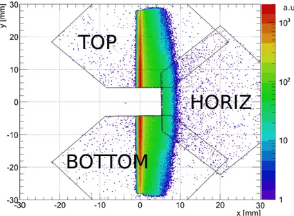
precision σ(∆t) ∼50 ps for the measurement of the proton track timing is required. The track distribution at the position of the timing detectors due to diffractive events and to overlapping background is not uniform and has been measured from RP tracking data, see figure 2. The average number of particles per bunch crossing in one of the RP is about 0.2 (including the beam background) at hµi = 0.5 [15].
Figure 2. The distribution of the particles traversing the RP plane at 220m with the TOF detector to be
installed in top and bottom RP for β∗ = 90 m optics. The TOF detectors will be installed in top and
bottom RPs.
The detector has to be segmented into pixels to minimize the occupancy2 of each cell. To
guarantee uniform occupancy in the detector, a pattern with pixels of different sizes has been simulated [15] and optimized in order to minimize the inefficiency due to the simultaneous presence of two hits in the same pixel. The optimized detector geometry with eight diamond plates obtained
2017 JINST 12 P03007
for a high-β∗ optics configuration at hµi= 0.5 is shown in figure3. The pixel size in the vertical
direction y varies by almost a factor six from 0.7 mm to 4.2 mm.
At hµi = 0.5, the inefficiency introduced by the pileup, as calculated with a MC which also take into account the beam halo contribution [15], is approximately 0.6%.
A reduced geometry has been adopted to build the prototype described here: it contains only four diamond plates and is shown in figure4. The four diamond single-pixel plates that are not included would cover only an extra 10% of acceptance.
Figure 3. Optimized layout of the detector pixels. On the right its position during physics data taking is
outlined on the track distribution of figure2.
Figure 4. Layout and dimensions of the pixels of the TOTEM timing detectors implemented and described
2017 JINST 12 P03007
One detector package contains four identical planes, each equipped with four plates of 4.5 × 4.5 mm2and 500 µm thick scCVD diamond metalized with a pattern of one, two or four pixels. If
one can build a single sensor capable of measuring with a time precision of the order of 100 ps, then with time measurements from four detectors one reaches the required overall time precision of about 50 ps. With such a precision for the measurement of the proton track timing the longitudinal interaction vertex can be determined with an uncertainty of ∼1 cm.
After some preliminary measurements in a test beam with a diamond sensor assembled with electronics of preliminary design, we saw that scCVD diamond detectors with a custom-built amplifier would match all the requirements of the timing detector needed for the TOTEM upgrade. With an appropriate metalization, one obtains a good contact to the face of the diamond sensor; it is fairly easy (fast and economical) then to implement a pattern with pixels of different sizes on a diamond crystal surface by means of a simple metalization. Due to the extremely high impedance of the diamond material, the difference in pixel size will barely affect the time response of the signal. Diamond sensors show also a better radiation hardness [16] and shorter charge collection times than other semiconductor sensors [17,18].
Additional technical requirements were taken into account to design a detector system that could be implemented and properly function in the high radiation environment of the LHC tunnel. In the following sections we detail the studies performed to ensure that scCVD diamond detectors will be able to meet the timing precision required by the physics program.
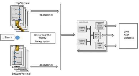
The TOF system main blocks which will be described in detail in the following sections is shown in figure5. x12 x12 x12 x12 x12 x12 Top Vertical 48 channel Bottom Vertical DAQ AND CONTROL One arm of the
TOTEM timing system bo ard Pre-a mplifie hape x1 x4 Hybrid A r S r 2 fie mp r
4 Hyb rid boar d Shaper Ampli Pre-a x12 x FPGA (SF2) Optical link (GOH) Slow control (CCUM) SAMPIC mezz. SAMPIC mezz. Readout board x3 48 channel p Beam
Figure 5. The TOF system for the TOTEM Vertical RP upgrade.
3.2 The diamond sensors
The use of detector grade scCVD diamond for use in particle detectors has been proposed in the past and extensively studied [18]. It is an ideal material for detecting particles due to its high electron and hole mobility and >99% charge collection efficiency.
2017 JINST 12 P03007
These detectors are now widely used in many specific applications and experiments, albeit still on a small scale. The availability on the market of detector grade scCVD diamond detectors of different sizes and thicknesses has greatly improved in recent years. Several companies3offer
custom sizes and thicknesses with reasonable delivery time.
3.3 Diamond crystal characterization
Electrodes on both sides are needed to collect the charges and read out the electric signal. Thin metal layers on both the top and bottom surface of the crystal generate the proper field and allow for connection to the amplifier. However, making a good ohmic electrical contact with the crystal structure is a delicate process. Metalization of the pixels on the surface of the diamond in some instances led to poor collection of charge or to a particle-rate dependent reduction of the charge collection [18]. The occurrence of ‘charging’ and ‘radiation’ damage of the diamond sensors has also been studied in high fluence High Energy Physics experiments, see for example [19].
The metalization area for the TOTEM plates covers 4.2 × 4.2 mm2 leaving a non-metalized
border region of 150 µm in order to avoid enhancement of surface leakage currents and discharges through the diamond edge. The metalization mask is aligned with better than 100µm precision on the diamond plate. When more than one pixel is present on one plate, the non metalized separation between pixels is 100µm. The diamond plates (four are needed per hybrid) are glued on the hybrid PCB in contact to each other and one may consider their maximum distance to be less than 50µm. Often the metalization processes are company specific and confidential. We have tested and compared different metalization techniques for the diamond sensors as suggested and provided by:
• GSI4(Cr-50 nm + Au-150 nm)
• Applied Diamond Inc. (U.S.A.)5(Cr-50 nm + Au-150 nm)
• PRISM6(100 nm of 10% Ti and 90% W alloy).
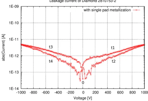
After a preliminary optical inspection with the microscope to check for small defects and missing or non-uniform metalization, the TOTEM high purity <100> orientation scCVD diamond plates have been checked for leakage current and stable signal current.
Each diamond plate is characterized in a specifically built IV setup. The current is measured for both polarities while increasing the HV to 1 kV in steps of 10 V and then the time stability of the current is checked during a period of the order of one hour. The leakage current versus voltage (IV curve) for one diamond and for both polarities are shown in figure6; t1 (0 V to 1 kV), t2 (1 kV to 0 V), t3(0 V to −1 kV) and t4(−1 kV to 0 V) in the figure identify the order in time of the measurements of the four curves.
More than 80 % of the TOTEM scCVD diamond metalized plates reached 1 kV with a leakage current of less than 1 nA; the ones with larger leakage current were discarded.
The signal stability in time, an indicator of the metalization quality, was measured using a
90Sr β radioactive source of approximately 36 MBq activity. Tests of detectors with different
3Element Six Ltd., http://www.e6.com King’s Ride Park, Ascot, Berkshire SL5 8BP, U.K., Diam2Tek,
http://www.diam2tek.eu, Irma-Feldweg-Straße 8, 75179 Pforzheim, Germany, among few others. 4http://www.gsi.de.
5http://usapplieddiamond.com/.
2017 JINST 12 P03007
Figure 6. Leakage current versus voltage for a one pixel diamond plate. t1, t2, t3 and t4 in the figure identify
the order in time of the measurements of the four curves.
metalization techniques and providers in identical conditions show similar performance in terms of charge collection and efficiency, both with radioactive sources and with minimum ionizing particles see also section4.1. Figure7shows the time stability of the signal current of two diamond detectors under irradiation from a radioactive β-source; the rate during these tests was approximately 10 kHz per pixel. The red curve shows the current measurement with the radioactive source removed at ∼2000 s and restored at ∼ 2800 s.
3.4 Electronics
Diamond sensors have the advantage of higher radiation hardness, lower noise and a faster charge collection than silicon sensors. However, for equal thickness the amount of charge released by a Minimum Ionizing Particle (MIP) in the diamond is lower than for silicon or germanium: only 2.9 fC are released by a MIP in a 500 µm diamond plate and a low noise amplifier is needed to keep the S/N ratio large enough.
The front end electronics design must be a compromise between speed and low noise.
Considering that the diamond resistivity is very high, the main source of noise will come from the first stage of the amplifier. For optimal energy transfer from the source to the input of the amplifier the impedances must match. That implies a high input impedance for the first stage of the amplifier, which is not the optimal choice from the Electromagnetic Compatibility (EMC) point of view. The front-end hybrid was tested in the CERN irradiation facility. After an irradiation of ∼ 5 × 10¹⁵ protons/cm2 it still detected MIP properly. Present data obtained from running
the experiment in previous years indicates that where the Read Out (RO) board will be installed, approximately two meters from the beam pipe, radiation rates are much smaller than in the RP; the RO board is designed to sustain such radiation doses.
2017 JINST 12 P03007
Figure 7. Stability of the signal currents over time for two different metalized crystals biased at 1kV
when exposed to a90Sr radioactive β-source, which indicates the quality of both the metalization and the
crystal itself.
3.4.1 The amplifier
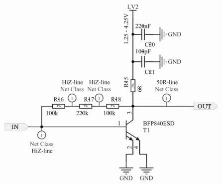
The amplification chain designed for TOTEM consists of a transconductance preamplifier followed by a single stage voltage amplifier (ABA) and by a booster which also shapes the analogue voltage output signal. The three parts of the amplification chain are shown in the figures8,9and10. This design has been adapted from the HADES Collaboration [20,21] amplifier.
2017 JINST 12 P03007
A good description for the diamond signal for the typical bias value used here is a triangular current pulse with a maximum amplitude of ∼ 1 µA, a rising edge of ∼ 2 ps and a falling edge of ∼ 5 ns.
The preamplifier, a SiGe BJT with low-capacitance feedback in a common emitter configura-tion, see figure8, should be as close as possible to the sensor, at most 1 cm away. The total input capacitance is given by the diamond capacitance (0.2 to 2 pF depending on the pixel size), by the connection of the diamond to the transistor base (approximately 0.2 pF when using 25 µm diameter wires) and by the parasitic capacitance of the transistor (about 0.4 pF). The input impedance for this configuration is a few kΩ while the capacitance seen by the signal source is low, which guar-antees a high signal to noise ratio (S/N). The choice of the feedback and collector resistances of the preamplifier has been optimized by TOTEM in order to keep the time precision around 100 ps also for the electrodes with the largest capacitance (∼2 pF). The preamplifier has a maximum current gain of 45 dB at low frequency and of 93 dB at 200 MHz.
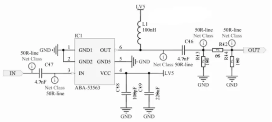
The signal from the first stage is fed to the second stage (Figure9) built around a broadband amplifier, the Avago ABA-53563 chip.
Figure 9. The ABA stage of the TOTEM timing detector signal amplification chain.
The optimization of the bias network of the ABA-53563 amplifier was performed in order to obtain an undistorted phase and gain response. This circuit has an almost flat power gain over the frequency range of interest and a noise degradation factor of 3.5 dB. The amplifier is suitably matched on input and output to 50 Ω and is unconditionally stable. The main advantage of the ABA amplifier chip is a constant group delay which means a low shape distortion of the input signal.
An attenuator is inserted between this amplification stage and the booster stage to prevent saturation for the largest signals and to ensure a better matching of the two stages; the attenuator between the amplifier and the booster was set to 10 dB after tests for optimum performance. The shaping stage is composed of two wide-band BJT transistors NPX BFG425W. The first booster stage defines the shaping time of the signal, via the RLC circuit between the collector and the feedback of the transistor. The shaper has a power gain of 53 dB at 200 MHz and an effective noise bandwidth of about 425 MHz. The rise time from the last stage is about 1.7 ns and the max voltage (before saturation) is 2.7 V, values that are adequate for transmission without degradation by approximately 2 m of coaxial cable. For the specified input and supply voltage the RMS noise on the output is ∼ 20 mV.
2017 JINST 12 P03007
The schematic of the booster stage of the amplifier of the TOTEM timing detector is reproduced in figure10.
Figure 10. The booster stage of the TOTEM timing detector signal amplification chain that both amplifies
and shapes the signal.
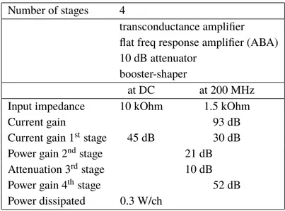
Table1summarizes the main parameters of the electronics.
Table 1. Characteristics of the TOTEM amplifier.
Number of stages 4
transconductance amplifier flat freq response amplifier (ABA) 10 dB attenuator
booster-shaper
at DC at 200 MHz Input impedance 10 kOhm 1.5 kOhm
Current gain 93 dB
Current gain 1ststage 45 dB 30 dB
Power gain 2ndstage 21 dB
Attenuation 3rdstage 10 dB
Power gain 4thstage 52 dB
Power dissipated 0.3 W/ch
3.4.2 The hybrid
The hybrid board to accommodate both the electronics and the detectors is a four-layer board of Rogers RO4350B and RO4450F7 low-loss materials ideal for RF applications and also a very
2017 JINST 12 P03007
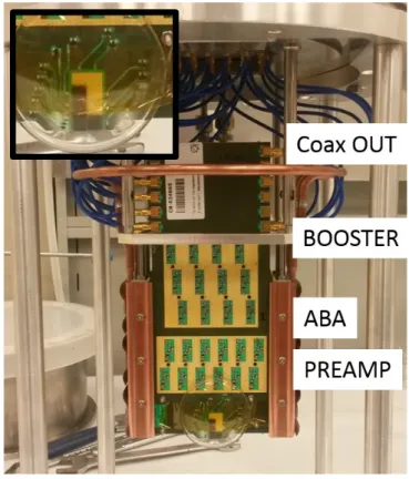
good insulator for the HV bias of at least 700 V required by the diamonds. The detectors are positioned and aligned with a precision better than 0.1 mm on this board and glued with silver-filled, electrically conductive epoxy adhesive.8 The picture of a timing detector plane designed for
twelve channels hybrid and four diamond plates per hybrid is shown in figure11, where the three hybrid amplification stages are indicated; the High Voltage (HV) pad onto which the diamonds are glued is easily identified.
Figure 11. Picture of one detector package in which the first of the four hybrid boards is visible: in the inset
a close-up of the four diamond crystals. Starting from the bottom of the board, one can identify the three amplifications stages: the preamplifier stage (“PREAMP”), the ABA stage (“ABA”) and the booster stage (“BOOSTER”). On the top of the picture one can see the coaxial output cables (“Coax OUT”).
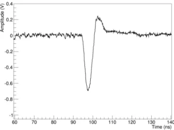
An output signal obtained with a MIP of average amplitude from one channel of the hybrid is shown in figure12.
3.4.3 Mechanical challenges
The detector packages (four hybrids) are in a vacuum of about 40 mbar that is required to minimize the deformation of the thin window of the RP that separates the detectors from the LHC circulating beam. The vacuum acts also as a heat insulator, and a heat exchanger is necessary to cool the detector and the RP itself.
The analog signals are sent from the hybrid inside the RP vacuum to the digitizer placed outside of the RP vacuum vessel at a distance of 2 m. Special care has been taken to to minimize
2017 JINST 12 P03007
Figure 12. Typical output signal of the hybrid for a MIP.
the reflections of the signal with a special flange equipped with 50 Ω SMP coaxial vacuum feed-through.9 Vacuum also imposes special care in routing the HV to the detectors as will be described
later in section5.1.
The four hybrids in one detector package are kept at a distance of 1 cm from each other in a precision mechanical support that integrates also the cooling system. The support ensures the precise positioning of the edge of the sensor with respect to the 200 µm thick ‘thin RP window’: the presence of the thin window and the precise positioning of the detector near it are features of high importance for the physics measurement. Before the installation in the RP, the position of the edge of the diamond mounted closest to the RP thin window, hence to the circulating beam, is measured with a laser with a precision of 10 µm. The alignment of the board on the support is then tuned to leave a safety margin of 150 µm between the detector and the thin window. The material budget of one hybrid intercepting the beam is dominated by the Roger material (1.3 mm), inner copper planes (0.2 mm) and diamond sensor (0.5 mm). For a hybrid plane, whose thickness is about x=1.8 mm, the total radiation length is about x/X0=0.02 and the total interaction length is about x/Λ =0.003.
3.5 Digitization: the SAMPIC chip
The precise measurement of the particle crossing time is obtained by digitizing the analog signals with a SAMpler for PICosecond time (SAMPIC) chip that gives a fast response similar to the one of a state-of-the-art TDC and the versatility of a waveform digitizer to perform accurate timing measurements. The input bandwidth is 1.5 GHz, the ADC precision is 11 bits and the unit may operate with a sampling frequency up to 10 GSa/s.
The SAMPIC chip has been designed by a collaboration between CEA/IRFU/SEDI, Saclay and CNRS/LAL/SERDI, Orsay [22,23] and named ‘Waveform and Time to Digital Converter’ (WTDC) multichannel chip. Each channel associates a Delay Line Loop-based (DLL) TDC providing a raw time with an ultrafast analog memory allowing the extraction of precise timing and other parameters
9SMP standard connectors vacuum feed-through provided bySolid Sealing Technology, Inc. 44 Dalliba Avenue
2017 JINST 12 P03007
from the pulse. Each channel also integrates a discriminator that can trigger itself independently or participate in a more complex trigger [24]. After triggering, the analog voltages are digitized by an on-chip ADC and only the data corresponding to a region of interest are transferred serially to the DAQ. The association of the raw and fine timings permits to achieve a timing precision of a few ps RMS.
Each channel is sampled through a 64 cell Delay Locked Loop (DLL) based memory. When the acquisition is triggered, the sampling is stopped and the sampled values are digitized using a Wilkinson ADC. The calibration procedure of the SAMPIC ADC is automatically done by the control software sending to each input a ramp of known voltages, provided by accessory electronics on the mezzanine, and measuring the digitized value. A polynomial curve is used to compensate for non-linearities. The small variation of the internal length of the delay lines can be calibrated with an externally generated sine wave and by measuring the deformation of the digitized signal; a future version of the mezzanine will integrate a signal generator to automate this second calibration. The time information is computed off-line from the digitized pulse using smart algorithms like constant fraction discrimination and fast cross-correlation.
A specifically designed TOTEM motherboard for synchronization of the acquired data with the TOTEM trigger and DAQ system is equipped with a mezzanine board with a SAMPIC chip mounted on it.
3.6 Clock distribution and DAQ board
To measure precisely on each side of the interaction point the arrival times of the protons and their difference, it is necessary to send a common picosecond range precision time reference signal to the detectors.
The TOTEM clock distribution design is adapted from the “Universal Picosecond Timing System”, developed for FAIR at GSI [25]. The TOTEM clock distribution system, based on an optical network, uses dense wavelength division multiplex (DWDM) technique to transmit two reference clock signals from the counting room to a grid of receivers near the detectors. The variation in the delay in the propagation of the signal is constantly measured in the central system by monitoring a signal reflected back from each station; this allows to control all the transmission systematic effects and keep the jitter below 5 ps. A full prototype of the clock distribution system has been assembled and is under final tests.
The information from the TOF detectors is collected by a dedicated board, built around the radiation tolerant Microsemi Soc FPGA M2S150-FCG1152.10 The board receives the TOF
signals digitized by the SAMPIC, builds the event data frame and sends the formatted data to the existing DAQ [13].
The board also controls the SAMPIC and as an example, sets the thresholds of the channels. The expected rate of timing detector hits in the vertical RPs is expected to be < 100 kHz per plane, which can be handled by the SAMPIC digitizer.
10Microsemi Corporation Corporate Headquarters, http://www.microsemi.com, One Enterprise Aliso Viejo, CA
2017 JINST 12 P03007
4 Tests and detector performance
In the process of designing the timing detectors, extensive tests have been performed with particle beams, initially to characterize the diamond sensors and to define the best design for the front end electronics and then to perform the check of the fully assembled prototype before its installation in the LHC.
4.1 Efficiency of the segmented diamond detector
Efficiency measurements of a diamond sensor with four pixels (strips) have been performed with a prototype board on a mixed pion and electron beam at DESY where a tracking telescope was available. To measure the efficiency the tracks have been reconstructed with the DATURA tracking telescope11composed of six silicon pixel detection planes. Figure13shows the Device Under Test
DUT
Figure 13. Setup of the DATURA telescope. Tracks are independently reconstructed on each arm.
(DUT) between two sets of three MIMOSA-2612silicon pixel detectors. These CMOS pixel sensors
are 50 µm thick with an active area of 21.2 × 10.6 mm2subdivided into 1152 columns of 576 pixels
each, i.e. a segmentation with a pitch of ∼ 18.4 µm, and a final precision of ∼ 5 µm for each plane. The off-line algorithm determines the impact point of the particle in the diamond detector reconstructing the track independently in each arm of the telescope thus allowing to consider the effect of possible multiple scattering in the DUT. This feature is particularly useful when working with electrons.
The measurements were performed with three hybrid boards, two equipped with single pixel diamonds and one with a segmented diamond. The four pixel sensor was installed between the two arms of the tracking telescope while the single pixel ones were placed downstream of the tracker. The sensors have been described in detail in section3.3. The two single pixel sensors were provided by CIVIDEC13and Element6. The detectors tested had been metalized by CIVIDEC and
by PRISM, the Princeton University laboratory. The diamond plates with four pixels foreseen for the vertical upgrade were metalized by the GSI, Darmstadt, Germany.
The efficiency is measured by comparing the position of a reconstructed track with the presence of a signal in one pixel. Given the high precision provided by the tracker, it was also possible to perform a two-dimensional scan of the diamond.
A uniform efficiency above 98% has been measured over a diamond detector, see figure14. The measurements of efficiency in the inter-pixel area are shown in figure15for the projection of the efficiency on the y axis. Getting closer to the thin inter-pixel area (0.1 mm wide),14 the
efficiency diminishes slowly while it starts increasing for the adjacent pixel due to charge sharing.
11DESY Advanced Telescope Using Readout Acceleration built as part of the EUDET\AIDA project. 12https://twiki.cern.ch/twiki/bin/view/MimosaTelescope/WebHome.
13CIVIDEC Instrumentation GmbH, Schottengasse 3A/1/41, A – 1010 Vienna, Austria. 14The geometrical region where the metalization is missing.
2017 JINST 12 P03007
Figure 14. The particle detection efficiency of the diamond detector. The statistical error on each point
is 5–10%.
Figure 15. Efficiency as a function of the position for two neighboring pixels separated by 0.1 mm. The
position of the hit is defined by tracks reconstructed from silicon telescope data. A 1–2% inefficiency can be attributed to the data acquisition system used for the test.
It is worth noting that the efficiency of one pixel remains always higher than 80% in the inter-pixel area.
In the inter-pixel area we have therefore two pixels that are able to detect the particle, and the overall combined efficiency becomes ∼96%. Still, for the particles traversing the lower efficiency area, one expects a worse time precision, since the amount of charge collected from the pixel electrode is lower. With a tracker detector associated to the timing detector, corrections based on the collected charge from both pixels can still be performed to reach the nominal precision.
2017 JINST 12 P03007
Figure 16. Comparison of the S/N of “Strip A” (a pixel with 0.29 pF) and CIVIDEC (2 pF). The number of
entries of each histogram are rescaled for better visualization of the signal region.
Figure 16 shows, superimposed and appropriately rescaled for comparison, the S/N for the pixel with the smallest and largest capacitance. The Signal to Noise ratio (S/N) obtained in these tests ranges between 20 and 35 with a small dependence on the pixel capacitance; the rise time of the pulse is about 1.7 ns.
4.2 Time precision
Time precision measurements with two diamond boards equipped with the final electronics were performed first in a test beam of 5.6 GeV electrons at DESY, and repeated later in a 180 GeV π+
beam at the CERN SPS. The two tests gave consistent results.
During these measurements performed at atmospheric pressure, the diamonds were biased at 700V. The data acquisition was performed with an Agilent DSO9254A oscilloscope (8 bits, 20 GSa/s), and the waveforms were then analyzed off-line using different algorithms. The time precision of a single detector is evaluated from the difference of the arrival time of a Minimum Ionizing Particle (MIP) traversing two diamond planes. No external time reference was used, only signals from two hybrids, with all the channels equipped with the final electronics. The time precision of the different pixels covers an interval between 80 < σt < 108 ps and correlates with
the pixel capacitance that ranges between 0.29 < C < 2 pF. Figure17shows the time precision as a function of the pixel capacitance; these results are summarized in table2. Pixels from different diamond sensors with the same capacitance show, within 5 ps, a similar time precision.
Figure 18shows the time difference distribution measured with the small pixel and the large pixel sensor.
The charge collection time, hence the peak current, depends on the drift velocity of the charge carriers. We observe that, due to non-saturation of the carriers’ drift velocity in diamonds [17,18], the time precision improves with increasing HV: tests have been repeated for different biasing
2017 JINST 12 P03007
Figure 17. Time precision as a function of the pixel capacitance and hence the detector area (after electronics
optimization).
Table 2. Summary of the results obtained for different sizes of the pixel sensitive area. Uncertainties of
the order of 5% were estimated by looking at the response of different electronic channels with pixels of the same capacitance.
Sensor Pixel area C σt Ampl. Rise Time S/N
[mm2] [pF] [V] [ns] Strip A 0.7 × 4.2 0.29 80 0.74 1.48 30 Strip B 0.83 × 4.2 0.34 85 0.70 1.51 31 Strip C 1.02 × 4.2 0.42 87 0.70 1.48 30 Strip D 1.35 × 4.2 0.56 102 0.62 1.49 28 One pixel 4.2 × 4.2 2 108 0.39 1.56 18
voltages up to 700 V or fields up to 1.4 V /µm. Above this value, the leakage current of some diamond sensors increased and the overall time precision did not improve further.
The measurements reported in figure17demonstrate that the ∼ 100 ps design precision needed for the project had been reached. Measurements performed in similar conditions on a particle beam at CERN show that the time precision obtained using the SAMPIC digitizer is compatible within less than 5 ps with the one obtained with the high bandwidth oscilloscope.
5 Detector package integration and installation
The detector package is assembled from four hybrids mounted and aligned on the same mechanical structure. The system must be able to work properly in the very specific environment of the TOTEM RP in the LHC. We describe now some technical system issues that imposed additional requirement on the detector.
2017 JINST 12 P03007
Figure 18. Measured time difference between Strip A (0.29 pF) of a four pixel sensor and a one pixel
(2.0 pF) sensor.
5.1 The HV distribution
To measure protons very close to the LHC beam axis, detectors must be installed in RPs, which are under moderate vacuum. Therefore special attention was dedicated to the design of the HV distribution for the diamond crystals.
Systematic tests of final prototype hybrids under various vacuum conditions and for above-nominal operating HV values were performed to test the quality of the system under HV and vacuum. When the onset of a discharge was seen from the current drawn by the HV power supply, a visual check allowed to identify the location where most likely the discharge had taken place. To reduce the probability of HV discharges under the moderate vacuum operation conditions, a specific layer of the hybrid board (the 5th layer) was solely dedicated to the routing of the HV distribution
and the blocking capacitors have been positioned in regions free of other components. The hybrid board, before adding the diamonds was tested to reach at least 1200 V without discharges. Once the diamonds were properly positioned, at 400 V one started to observe lateral discharges between the two faces of the diamond sensors. This problem was solved as detailed in section5.2.
The pixels are connected to the input of the amplifier, approximately 1 cm away, with an aluminum bonding wire of 150 µm diameter, which is thicker than the usual 25 µm diameter. Tests have also been performed to ensure that the small increase of capacitance and inductance due to a larger than usual wire diameter does not degrade the time precision of the detector.
5.2 The coating
On the hybrid board, the edges of each diamond sensor and all the components carrying HV near them have been specifically protected by adding a protective high volume resistivity Silicone coating compound.15 This operation had to be performed after the bonding and was studied in collaboration
with the company Mipot16that has then treated all our boards.
15Dow Corning SE918L.
2017 JINST 12 P03007
Final tests have been performed on all the eight boards treated with this feature and have shown that one could safely bring the HV to 700 V at the required operating pressure of about 40 mbar.
5.3 Vacuum operation and cooling
The necessity to encase the detector package in a closed metallic container (the vacuum vessel) is a source of unwanted noise and feedback between the hybrids. Measurements with a fully equipped detector package have shown a very large level of interference between the boards that induced easily unwanted oscillations. To damp any possibility of undesired radiative interference, the vacuum vessel is lined with 2 mm EMI suppressor shielding from KEMET.17
To operate the electronics in the vacuum vessel all the dissipated power must be removed by an efficient and stable cooling system. In fact, the amplifier was designed for operation at room temperature. The system must evacuate the power dissipated by the electronics and the heating of the RP vacuum pipe due to the beam RF pick up which increases at high luminosity. The RP are equipped with an evaporative cooling system as already used for the silicon TOTEM strip detectors. It has been set to keep the temperature stable at 25◦C.
5.4 Commissioning and operation in the LHC tunnel
The assembled system, installed in a Roman Pot container and cooled as if it were in the tunnel, was commissioned and checked on a particle test beam on the surface prior to the installation in the LHC tunnel in the November 2015 technical stop, see figure19.
The timing detector was operated for 48 hours during an LHC pp run at√s= 5 TeV: the RPs were retracted in the ‘garage’ position, and the observed signal rate was ∼10–100 Hz/pixel.
In the LHC, with the diamonds operated at an HV of 500 V and with the digitization performed by a SAMPIC unit, the time precision obtained for the small capacitance pixels was ∼ 90 ps, see figure20. This is compatible with the 80 ps obtained in previous tests with a higher HV value.
The noise of the electronic board at T = 25◦Cwas 15–28 mV RMS, compatible with the one
previously measured.
6 Conclusions
The design of the TOTEM TOF diamond detectors for the upgrade of the vertical RPs has been described. The sensors have been characterized in several test beams and have shown a time precision better than 100 ps per plane for MIPs, and for electrode capacitance less than 1 pF. The detection efficiency is larger than 98% in the metalized region. The digitization of the signal, made with the SAMPIC chip introduces a measured negligible deterioration of the time precision. The first TOF prototype with four diamond planes read out by SAMPIC has been installed in the LHC at the beginning of November 2015. A time precision of about 90 ps per plane has been found, compatible with the project specification. The clock distribution system, designed to guarantee a jitter control to better than 1 ps precision, has been assembled in the laboratory.
Later, in June 2016, two modules of four diamond planes have been installed in the LHC and are now operated at the highest LHC luminosity obtained so far (1.4 × 1034cm−2s−1) as part of the
CT-PPS project [26].
2017 JINST 12 P03007
Figure 19. The prototype TOTEM timing detector installed in the LHC tunnel in November 2015.
2017 JINST 12 P03007
Acknowledgments
We thank S. Baud, D. Druzhkin and R. Stepanovich for the invaluable and efficient help during the development and installation of the detectors and F. Manolescu and I. Mcgill of the CERN bonding lab for their excellent bonding work on many hybrid boards and prototypes. The efficiency measurements reported in this work have been obtained at the test beam facility at DESY, a member of the Helmholtz Association (HGF). We are grateful to GSI and to PRISM (Princeton) for having provided help with the diamond metalizations. We thank the HADES colleagues for the useful discussions and for allowing us to test one of their detectors.
This work was supported by the institutions listed on the front page and also by the Magnus Ehrnrooth foundation (Finland), the Waldemar von Frenckell foundation (Finland), the Academy of Finland, the Finnish Academy of Science and Letters (The Vilho, Yrjö and Kalle Väisälä Fund), the OTKA grant NK 101438 (Hungary) and also by the project LM2015058 from the Czech Ministry of Education Youth and Sports.
Individuals have received support from Nylands nation vid Helsingfors universitet (Finland), the Swedish Cultural Foundation in Finlandand and the MŠMT ČR (Czech Republic).
This project has received funding from the European Union’s Horizon 202018 Research and
Innovation program under grant agreement No 654168. Support for some of us to travel to CERN for the detector tests on the beam was provided by 2020-CERN-TB-2015-10 and AIDA-2020-CERN-TB-2016-11.
References
[1] G. Antchev et al., First measurement of the total proton-proton cross section at the LHC energy of√ s= 7 TeV,Europhys. Lett. 96(2011) 21002[arXiv:1110.1395].
[2] TOTEM collaboration, G. Antchev et al., Luminosity-independent measurements of total, elastic and
inelastic cross-sections at√s= 7 TeV,Europhys. Lett. 101(2013) 21004.
[3] TOTEM collaboration, G. Antchev et al., Measurement of proton-proton elastic scattering and total
cross-section at√s= 7 TeV,Europhys. Lett. 101(2013) 21002 CERN-PH-EP-2012-239.
[4] TOTEM collaboration, G. Antchev et al., Luminosity-Independent Measurement of the Proton-Proton
Total Cross section at√s= 8 TeV,Phys. Rev. Lett. 111(2013) 012001.
[5] TOTEM collaboration, G. Antchev et al., Measurement of proton-proton inelastic scattering
cross-section at√s= 7 TeV,Europhys. Lett. 101(2013) 21003.
[6] M.G. Ryskin, A.D. Martin and V.A. Khoze, Soft diffraction at the LHC: A partonic interpretation, Eur. Phys. J. C 54(2008) 199[arXiv:0710.2494].
[7] E. Gotsman, E. Levin, U. Maor and J.S. Miller, A QCD motivated model for soft interactions at high
energies,Eur. Phys. J. C 57(2008) 689[arXiv:0805.2799].
[8] S. Ostapchenko, On the model dependence of the relation between minimum-bias and inelastic
proton-proton cross sections,Phys. Lett. B 703(2011) 588[arXiv:1103.5684].
[9] TOTEM collaboration, Addendum to the TOTEM TDR: Timing Measurements in the Vertical Roman
Pots of the TOTEM Experiment LHCC document CERN-LHCC-2014-020 including
questions/answers from/to the referees,CERN-LHCC-2014-024, TOTEM-TDR-002-ADD-1 (2014).
2017 JINST 12 P03007
[10] TOTEM collaboration, Timing Measurements in the Vertical Roman Pots of the TOTEM Experiment,CERN-LHCC-2014-020TOTEM-TDR-002 (2014).
[11] TOTEM collaboration, K. Österberg, Potential of central exclusive production studies in high β∗runs
at the LHC with CMS-TOTEM,Int. J. Mod. Phys. A 29(2014) 1446019.
[12] TOTEM collaboration, V. Berardi et al., Total cross-section, elastic scattering and diffraction
dissociation at the Large Hadron Collider at CERN: TOTEM Technical Design Report,
CERN-LHCC-2004-002and addendumCERN-LHCC-2004-020(2004).
[13] TOTEM collaboration, G. Anelli et al., The TOTEM experiment at the CERN Large Hadron Collider,
2008 JINST 3 S08007.
[14] G. Ruggiero et al., Characteristics of edgeless silicon detectors for the Roman Pots of the TOTEM
experiment at the LHC,Nucl. Instrum. Meth. A 604(2009) 242.
[15] M. Berretti, Performance studies of the Roman Pot timing detectors in the forward region of the IP5 at
LHC,CERN-TOTEM-NOTE-2014-001(2014).
[16] W. de Boer et al., Radiation hardness of diamond and silicon sensors compared,Phys. Status Solidi 204(2007) 3009[arXiv:0705.0171].
[17] H. Pernegger et al., Charge-carrier properties in synthetic single-crystal diamond measured with the
transient-current technique,J. Appl. Phys. 97(2005) 073704.
[18] M.Pomorski, Electronic properties of single crystal cvd diamond and its suitability for particle
detection in hadron physics experiments, Ph.D. Thesis, Wolfgang von Goethe University Frankfurt,
Germany (2008),http://www-norhdia.gsi.de/publications/pomorski_thesis_final_LQ.pdf. [19] M. Guthoff et al., Radiation damage in the diamond based beam condition monitors of the CMS
experiment at the Large Hadron Collider (LHC) at CERN,Nucl. Instrum. Meth. A 730(2013) 168.
[20] E. Berdermann et al., Diamond Start Detectors, in proceedings of the 2009 IEEE Nuclear Science
Symposium and Medical Imaging Conference (NSS/MIC 2009), pp. 407–411, (2009),
DOI:10.1109/NSSMIC.2009.5401672.
[21] M. Ciobanu et al., In-beam diamond start detectors,IEEE Trans. Nucl. Sci. 58(2011) 2073. [22] E. Delagnes, D. Breton, H. Grabas, J. Maalmi and P. Rusquart, Reaching a few picosecond timing
precision with the 16-channel digitizer and timestamper SAMPIC ASIC,Nucl. Instrum. Meth. A 787
(2015) 245.
[23] D. Breton et al., Measurements of timing resolution of ultra-fast silicon detectors with the SAMPIC
waveform digitizer,Nucl. Instrum. Meth. A 835(2016) 51[arXiv:1604.02385].
[24] E. Delagnes et al., The SAMPIC Waveform and Time to Digital Converter, proceedings of the 2014
IEEE Nuclear Science Symposium and Medical Imaging Conference (2014 NSS/MIC), and 21st
Symposium on Room-Temperature Semiconductor X-Ray and Gamma-Ray Detectors. Seattle, U.S.A.,
http://hal.in2p3.fr/in2p3-01082061.
[25] M. Bousonville and J. Rausch, Universal picosecond timing system for the facility for antiproton and
ion research,Phys. Rev. ST Accel. Beams 12(2009) 042801.
[26] M. Albrow et al., CMS-TOTEM Precision Proton Spectrometer,CERN-LHCC-2014-021