UNIVERSITA’ DEGLI STUDI DI MESSINA E UNIVERSITÀ
DI MOSTAGANEM
Dottorato di Ricerca in Fisica
XXIX ciclo
Study and Simulation of a
Nanoscale Structure of a Multi-gate
MOS Transistor
PhD Student: Dott. Nour El Islam Boukortt
Tutor: Prof. Salvatore Patanè
Tutor: Prof. Hadri Baghdad
Coordinator: Prof. Lorenzo Torrisi
SSD: FIS/03
2
Summary
Declaration ... 6 Publications ... 6 Abstract ... 7 Chapter I ... 8 CHAPTER I: Introduction ... 9 1.1 Work Overviews ... 9 1.2 Objectives ... 9 1.3 Project Definition ... 91.3.1 Understand the Devices ... 9
1.3.2 Learn the Usage of the Software Package ... 11
1.3.3 Simulate and Optimize Devices... 12
1.4 Thesis Structure Overview ... 13
Chapter II ... 14
Chapter II: FET Device Physics... 15
1. The metal-oxide-semiconductor-field-effect-transistor ... 15
1.1. The MOS capacitor ... 16
1.2. Threshold voltage... 20 1.3. Source-drain resistance ... 21 1.4. On-state current ... 21 1.5. Off-state current ... 23 1.6. Transconductance ... 26 1.7. Subthreshold slope ... 27
1.8. Drain induced barrier lowering (DIBL) ... 29
1.9. Mobility ... 31
2. The Silicon FET as a Nanoelectronic Device ... 31
2.1. What is Nanotechnology ? ... 31
2.2. Silicon material ... 32
2.3. Silicon FETs in the Nanometer Regime ... 33
2.4. The short channel effect ... 35
2.5. Channel control ... 35
2.6. Multi-gate transistors ... 36
3
3.1. Advantages of high-k oxides in electronics ... 51
4. Quantum Effects in FinFETs ... 56
4.1 Quantum Confinement ... 56
4.2 Quantum-Mechanical Tunneling ... 61
4.3 Ballistic Transport and Quantum Interference ... 61
Chapter III ... 63
CHAPTER III: FABRICATION AND SIMULATION ... 64
3.1 Silvaco’s TCAD Software ... 64
3.1.1 ATHENA ... 67 3.1.2 ATLAS ... 67 3.1.3 DECKBUILD ... 68 3.1.4 DEVEDIT ... 69 3.1.5 TONYPLOT ... 69 3.2 Physical models ... 69 3.2.1 Mobility models ... 69
3.2.2 Shirahata’s Mobility Model ... 70
3.2.3 Parallel Electric Field-Dependent Mobility ... 71
3.2.4 Generation-Recombination ... 71
3.2.5 Shockley-Read-Hall (SRH) Recombination ... 72
3.2.6 Band-to Band tunneling ... 73
3.3 Process Flow to Develop the Environment of Project ... 74
3.4 Fabrication process ... 75
3.4.1 Meshing ... 77
3.5 Device Simulation using Atlas ... 79
3.6 Device Simulation ... 80
3.6.1 IDS -VGS characteristics ... 80
3.6.2 Parameters Extraction ... 81
3.6.3. Effects of variations of the channel doping concentration ... 90
3.6.4. Effects of variations of the gate metal work function ... 96
3.6.5. The effects of gate dielectric material on electrical characteristics of n-FinFET device ... 101
3.6.6. The effects of temperature on electrical characteristics of n-FinFET device ... 105
3.6.7. Effect of Number of fins on electrical device characteristics ... 109
Conclusion ... 113
4
5
Acknowledgements
Firstly, I should like to thank my supervisors Prof. Hadri Baghdad and Prof. Salvatore Patanè. Without their guidance over the last 3 years, this thesis would not have been possible.
Secondly, a big thank you must go to Prof. Lorenzo Torrisi, Prof. Alina Caddemi, Prof. Giovanni Crupi, and Dr. Emanuele Cardillo (University of Messina, Italy) for their expertise and helpful discussions which lead to a very successful collaboration.
Of course a thank you must go to my dear colleagues and to all members in Silvaco Research Group for their help and advice.
My heartfelt and special thanks also go to my wonderful father for his love and his support over the years.
Last but not least, I should like to thank my family and friends, for their support and encouragement.
6
Declaration
This thesis is submitted to the University of Mostaganem and University of Messina in support of my application for the degree of Doctor of Philosophy.
Publications
N. Boukortt, B. Hadri, S. Patanè, A. Caddemi, and G. Crupi, ―Investigation on TG n-FinFET parameters by varying channel doping concentration and gate length‖ Silicon - Springer (in press).
N. Boukortt, B. Hadri, A. Caddemi, G. Crupi, and S. Patanè, ―The temperature dependence of electrical parameters of TG SOI n-FinFET‖ Trans. Electr. Electron. Mater. (in press).
N. Boukortt, B. Hadri, S. Patanè, A. Caddemi, and G. Crupi, ―Electrical Characteristics of 8-nm SOI n-FinFETs‖ Silicon - Springer (2016).
N. Boukortt, B. Hadri, and S. Patanè, ―Effects of high-k dielectric materials on electrical characteristics of DG n-FinFETs‖ IJCA (2016).
N. Boukortt, B. Hadri, and A. Caddemi, ―Simulation of a Nanoscale SOI TG n-FinFET‖ IJCA (2016).
N. Boukortt, A. Caddemi, E. Cardillo, G. Crupi, B. Hadri, and S. Patanè, ―Inverse Modeling of an AlGaAs/GaAs HEMT from DC and Microwave Measurements‖ 12th International Conference on Telecommunications in Modern Satellite, Cable and Broadcasting Services – TELSIKS, IEEE Proceeding Conference. (2015).
N. Boukortt, B. Hadri, L. Torrisi, S. Patanè, A. Caddemi, and G. Crupi ―Influence of gate dielectric materials on electrical characteristics of 3D DG n-FinFETs with different channel materials‖ Nanotech France 2015 International Conference Proceeding (2015).
N. Boukortt, B. Hadri, A. Caddemi, G. Crupi, and S. Patanè, ―3-D Simulation of Nanoscale SOI
n-FinFET at a Gate Length of 8 nm Using ATLAS SILVACO‖ Trans. Electr. Electron. Mater. 16, 2-7 (2015).
7
Abstract
To enable the advancement of Si based technology, necessary to increase computing power and the manufacture of more compact circuits, significant changes to the current MOS multi-gate transistor device are a necessity. Novel transistor architectures and materials are currently being researched vigorously. This thesis, on the electrical characterisation of multi-gate transistors displays detailed insight into the carrier transport and resulting performance limiting mechanisms. The results are composed of many parts. The impact of variations of the gate length, gate dielectric material, fin parameter, gate work function, doping concentration, and temperature on device characteristics are studied using ATLAS Silvaco device simulator. Simulation results for various gate lengths are reported and analyzed. As the quantum effects are pronounced in nanoscale devices, we have included these effects in our study and simulation. We have then compared the achieved results to classical simulations to assess their performance limits. Finally, a comparison of our results with recently published data is presented to confirm our study.
8
9
CHAPTER I: Introduction
1.1 Work OverviewsThe aim of this work was the optimization of MOS multi-gate transistor device performance using Semiconductor TCAD tools. Semiconductor TCAD (Semiconductor Technology Computer Aided Design) tools are computer programs which allow for the creation, fabrication, and simulation of semiconductor devices. These tools were used to optimize semiconductor devices for various applications.
During the course of this work, these programs were used to create simulations of the devices being worked on. These simulations provided the opportunity to study the effect of different device parameters on the overall device performance. Throughout the years, the devices were simulated and gradually the performance of each one was improved, until an optimal device configuration was created for the particular applications.
1.2 Objectives
The overall objective of this project was the optimization of the various semiconductor devices. In order to achieve this goal, several intermediate objectives were needed.
- Understand FET devices and the applications for which it is used - Learn and understand the use of Silvaco's TCAD software
- Create an initial device design using reference material from Silvaco's web-site - Generate benchmarks for initial device design
- Choose an application for which the device is to be optimized
- Vary device parameters and study resulting effects upon performance - Determine optimal values for FinFET device parameter
- Combine the optimal parameters into a final, fully optimized device
The accomplishment of each of these intermediate objectives was critical to the success of the work as a whole. All these objectives can be grouped under three main categories and are expanded upon in the following section.
1.3 Project Definition
1.3.1 Understand the Devices
First and foremost a basic understanding of the fabrication, operation, advantages, and applications of FET (Field Effect Transistor) device was needed before any simulations or optimizations could commence. This understanding of the devices was gained through extensive research conducted on each device. Various sources were consulted and the resultant understanding of the devices was key in the creation of optimized device configurations.
Two devices were selected for optimization during the course of this work. These devices are the SOI FinFET (Fin-Shaped Field Effect Transistor) device and the triple gate
10
FinFET device. An in-depth report on the research conducted can be found under each individual device section. For the purposes of the introduction, a general device overview is given.
FinFET technology is a new industry standard. This technology has been around for recent years, and the fabrication methods are continually improving, yet they are well established [1].
The cost and size are main advantages of FinFET devices. Since the technology is well established, fabrication methods have become relatively inexpensive. Also, the device itself is physically smaller than other technologies, allowing for the placement of more devices on a silicon wafer during fabrication. FinFET devices are mainly used in the creation of CMOS logic chips, which are at the heart of every computer [1]. An enhancement-type NMOS transistor was used during the course of this work which has high electron mobility and interfaces easily with low voltage positive logic compared to PMOS. Figure 1.1 shows the basic structure of this style FinFET device.
Figure 1.1 Physical structure of an enhancement-type n-FinFET transistor [1].
SOI (Silicon-On-Insulator) devices are a relatively new technology. Although the technology has been available since the 1960’s, SOI devices are only recently becoming commercially viable, due to the expense associated in producing the devices. SOI devices are an advancement of standard FinFET technology. The main difference between SOI and bulk technology is the inclusion of an insulating layer. SOI devices are created from a thin layer of silicon placed on top of a layer of insulating material [2]. This structure can be seen in Figure 1.1. Most often this material is silicon oxide, however other insulating materials are being tested, such as diamond, sapphire, and ruby. For this work, a buried oxide layer (BOX) of silicon dioxide was used for the creation and simulation of the SOI FinFET device [2].
The second technology for which optimization was pursued is the TG n-FinFET (Triple Gate n-FinFET) device. This device takes advantage of the buried oxide layer of a SOI device by adding a third gate above the device’s channel. This allows for greater control of the device switching, and opens the doors for great advances in device design. The FinFET
11
technology is by far the newest and most advanced semiconductor technology simulated during the course of this work, further explanation of this device and the others simulated during the work, can be found under the individual device sections.
Figure 1.2. Physical structure of an enhancement-type TG n-FinFET transistor [3].
1.3.2 Learn the Usage of the Software Package
Once a basic understanding of each device was acquired, and in some cases while research on the device was proceeding, the operation of the software package needed to be learned. The software package used for this project is Virtual Wafer Fab (VWF) package built by Silvaco International. VWF is a suite of software programs used to create a multi-functional environment for the simulation of semiconductor technology. Several different programs were learned and then used throughout the years, allowing for simulation of these devices on many different levels. After trying different programs in the suite, simulation efforts were focused on using ATHENA, ATLAS, DevEdit, and DeckBuild [4].
ATHENA is a framework program that integrates several smaller programs into a more complete process simulation tool. It is a modular program that combines one and two-dimensional simulations into a more complete package allowing for the simulation of a wide range of semiconductor fabrication processes. This program’s focus is upon the simulation of fabrication processes. In ATHENA, devices are created through simulation of the fabrication process [4].
ATLAS is a device simulation tool. The framework of ATLAS combines several one, two, and three-dimensional simulation tools into one comprehensive device simulation package. This allows for the simulation of a wide variety of modern semiconductor
12
technologies. Devices can be created in ATLAS through layout based simulation syntax; however the main focus of this program is simulation of the device once fabrication is complete [4].
DevEdit is a program that allows for structure editing, structure specification, and simulation grid generation. All of Silvaco’s programs use a mesh or grid to determine the level of detail that the simulation will generate in a specific area of the device, allowing users to cut down on simulation time by removing detail from areas with uniform or no reaction to performance simulations. The creation of these meshes is the main function of DevEdit, however it is also be used for the editing and specification of two and three-dimensional devices created with the VWF tools [4].
DeckBuild is the front-end GUI (Graphical User Interface) for Silvaco’s Virtual Wafer Fab programs. This program is the framework which ties together the wide range of process and device simulation tools available, and allows them to work together seamlessly and efficiently [4]. DeckBuild uses pull-down menus to generate syntax for the various programs, and provides basic simulation controls such as stop, pause, and restart. The use of ATHENA, ATLAS, and DevEdit are expanded upon in later sections of this thesis, DeckBuild was used for front-end simulation control in each case. In order to learn the use of these programs, many sources were consulted [4].
Various device examples are available through the Silvaco’s homepage. These examples and research material available through the company’s web-site and user manuals have been used as starting point to gain the basic knowledge of each program’s operation. Once this operational level of understanding was acquired, research into the effects of device parameters upon performance could begin.
1.3.3 Simulate and Optimize Devices
Once an understanding of the device and the software was obtained, the simulation and optimization of the devices could begin. The first step in optimization is the selection of an initial device configuration. Using reference material and example programs available through Silvaco’s homepage, initial device designs were created, taking into account the computing time. These initial configurations were designed to be simple, yet straightforward examples each device’s capabilities.
Once initial devices were selected, a goal for optimization was needed. It was decided that the devices would be optimized for low power, high-speed applications. In order to determine the optimal configuration, the ID vs. VGS curves were examined. A lowered threshold voltage and an increased transconductance became the optimization goals of the work. Improving these two parameters would produce a lowered operating voltage, and increased switching speed. Optimization for reducing the subthreshold swing, DIBL, and leakage current were three other objectives considered for the work. However, after further research both these goals were determined to be beyond the scope of this work, and were ultimately removed from the list of design goals.
13
Optimization of these devices using the TCAD tools requires many hours of lab simulation time. Several aspects of each device were selected for optimization. First each parameter was tested individually for its effect on device performance as a whole. Once several plots were obtained that indicated the particular parameter’s effect on device performance, improved values could then be selected for the device. Several simulations needed to be run to find improved values for each device parameter, until an optimal value was reached. After reaching the optimal value of each of the device parameters which should recombine them together into a single device, the simulation could begin to optimize based upon their combined effects and to ultimately produce an optimal device configuration.
1.4 Thesis Structure Overview
The remainder of this thesis focuses on each aspect of this research work in far more detail. Explanations the reasons for the choosing of each device structure used for simulation, the design methods used, detailed information about the function of each device, and step by step explanations of the steps taken during optimization. The MOS transistor is the first device discussed in this thesis due to the relative simplicity of the device. Once a basic understanding of the FET and the optimization approach for this device is grasped, the SOI devices become easier to understand. The SOI concepts are used as a foundation for understanding a new generation of FinFET devices.
14
15
Chapter II: FET Device Physics
The main components of an integrated circuit (IC) are Metal-oxide-semiconductor (MOS) transistors. MOS technology is used in microprocessors, microcontrollers, static RAM, SRAM cell, and other digital logic circuits. Also, it is used in a wide variety of analog circuits such as image sensors, data converters, and highly integrated transceivers for many types of applications [5]. Two important characteristics of the Complementary MOS (CMOS) technology are high noise immunity and low static power consumption. Significant power is only drawn when the transistors are switching between on and off states. Consequently, MOS circuitry dissipates less power and is denser than other implementations having the same functionality. As this advantage has grown and become more important, the vast majority of modern integrated circuit manufacturing is on CMOS processes. Currently, the appearance of smart devices such as smartphone, tablet, and laptop changes semiconductor market trends. The origin of smart devices was IBM Simon which was released in 1993 as a world first smart device as a convergence between mobile phone and PC [2, 5]. It included a schedule manager, address book, world clock, fax, games, and calculator etc. With evolutions, smart devices have been continuing like personal digital assistant, iPhone and Galaxy Tab etc. Especially after iPhone and Android smartphone has been released in the market, numerous smart applications which use simple user interface, global positioning system (GPS), motion sensors and Wi-Fi etc., play a role as a bridge between human and smart devices.
1. The metal-oxide-semiconductor-field-effect-transistor
A standard semiconductor MOSFET consists of a MOS capacitor with a highly doped source and drain region either side (Figure 2.1), each with a respective metal contact. These relatively simple devices can be p-channel (n-doped body with highly p-doped source and drain) or n-channel (p-doped body with highly n-doped source and drain). Figure 2.1 is a schematic of an n-channel MOSFET including the electrical connections. Note the source and p-type substrate are grounded. When Vgs < Vth, the p-type substrate is either in accumulation or depletion and no current can flow between the source and drain even when in the presence of the bias Vds. The MOSFET acts like two p-n junction diodes connected back to back (two p-n junction diodes). When Vgs>Vth, the semiconductor surface is inverted to n-type, forming a conducting channel between the n+ source and drain. When Vds is applied an electron current will flow from the source to the drain [6]. Increasing the gate bias increases the concentration of electrons at the semiconductor surface, and allows more current to flow [7].
16
The gate can therefore be used to modulate the current flow between source and drain, giving rise to the switching operation in integrated circuits.
Figure 2.1 Physical structure of the enhancement-type NMOS transistor:
(a) perspective view; (b) cross section [8].
1.1. The MOS capacitor
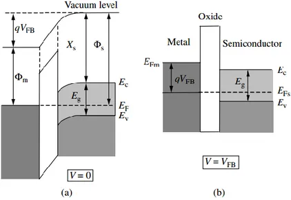
A MOS capacitor consists of a conducting metal layer (metal gate) on top of a dielectric grown or deposited on a semiconductor substrate, the bulk of which can be doped n-type (p-MOS capacitor) or p-type (n-MOS capacitor). The operation of an n-MOS capacitor under gate bias, Vgs is now considered. All potentials are with respect to the substrate/bulk which is grounded. At zero applied bias, the bending of the energy bands is ideally determined by the difference in the work functions of the metal and the semiconductor
17
(Band bending means a change in electric potential and therefore the existence of an electric field.) Oxide and interface trapped charges can also contribute to an appreciable amount of band bending [9, 10].
This band bending changes with the applied bias and the bands become flat when we apply the so-called flat-band voltage given by [11]:
VFB = (фm − фs)/q = (фm − Xs − Ec + EF)/q (2.1)
where фm and фs are the work functions of the metal and the semiconductor, respectively, Xs is the electron affinity for the semiconductor, Ec is the energy of the conduction band edge, and EF is the Fermi level at zero applied voltage. The different energies involved are indicated in Figure 2.2, where it presents typical band diagrams of a MOS capacitor at zero bias, and with the voltage V = VFB applied to the metal contact relative to the semiconductor– oxide interface.
Figure 2.2 Band diagrams of MOS capacitor (a) at zero bias and (b) with an applied voltage
equal to the flat-band voltage. The flat-band voltage is negative in this example [11].
In stationary conditions, no net current flows in the direction perpendicular to the interface, owing to the very high resistance of the dielectric layer. Hence, the Fermi level remains constant inside the semiconductor, irrespective of the biasing conditions [8]. Very little band bending occurs in the metal due to the abundance of free carriers. An n-MOS capacitor will enter the accumulation regime of operation when the voltage applied between the metal and the semiconductor is more negative than the flat-band voltage (Vfb <0). The negative bias raises the metal Fermi level (i.e. the potential energy of electrons) with respect
18
to the semiconductor Fermi level and creates an electric field from the substrate, through the oxide (just like an ordinary parallel plate capacitor) into the gate. Electrons in the gate are displaced towards the semiconductor and holes in the semiconductor displaced towards the gate. Figure 2.3a) shows the energy bands in accumulation. The field in the semiconductor causes the bands to bend upward. The Fermi level at the surface is now much closer to the valence band than the Fermi level in the bulk, corresponding to a much higher holes concentration at the surface than the equilibrium ones in the bulk. When Vgs > VFB, the capacitor will enter the depletion regime of operation. The positive bias lowers the metal Fermi level with respect to the semiconductor Fermi level. The electric field is now in the direction from the gate to the substrate. Holes in the semiconductor move away (depleted) from the interface, leaving a net negative charge from the acceptor ions. This is known as depletion charge. The bands in the semiconductor bend downwards. The valence band at the surface is now farther away from the Fermi level than the valance band in the bulk expressing the lower holes concentration at the surface than the equilibrium ones in the bulk. As Vgs increases, holes continue to be depleted from the interface leaving behind more acceptor ions resulting in more depletion charge and a wider depletion region. This continues until it becomes energetically favorable for electrons to populate the conduction band at the surface. The process of electrons populating the conduction band at the surface in a p-type semiconductor is known as surface inversion and the surface behaves like an n-type material. The resulting sheet of electrons at the surface is referred to as the inversion layer. At this point all holes are depleted from the surface and the depletion charge ceases to increase. Figure 2.2b) shows the energy band diagram when the MOS capacitor is in the inversion regime [8-10].
On the energy band diagram, the bands bend downward so much that at the surface, which the conduction band approaches the Fermi level expressing the much higher electron concentration. In the figure, the Fermi level at the surface is as far above the intrinsic level, Ei, as the Fermi level is below the intrinsic level in the bulk semiconductor. Thus the electron concentration at the surface is the same as the holes concentration in the semiconductor. This condition is known as the threshold inversion point and the corresponding gate voltage known as the threshold voltage, Vth. The additional field lines from the gate now terminate on the inversion charge rather than the depletion charge, thereby screening the semiconductor from any further band bending. When Vgs>Vth, we enter into strong inversion where more inversion charge will be generated whilst the band bending remains essentially constant [8].
19
Figure 2.3 a) n-MOS capacitor in accumulation and b) inversion [8].
The gate voltage at inversion is related to the voltage across the oxide (Vox), the semiconductor ψs, and flat-band voltage (VFB) which is an important parameter when analysing capacitance profiles as it marks the boundary between accumulation and depletion [8].
(2.2)
where Cox is the areal oxide capacitance and Qs is the areal total surface charge at the semiconductor-oxide interface, composed of the areal inversion and depletion charges, Qinv and Qdep respectively. It is common to express Qinv and Qdep, as inversion charge density Ninv and depletion charge density Ndep (normalised with respect to electron charge). ψs is the surface potential, is defined as the difference between the intrinsic Fermi-level (in V) at the surface and its bulk level. Note that the perturbations of the conduction band, valence band and intrinsic Fermi-level band are equal. The band perturbation potential as a function of distance perpendicular to the interface, ψ(z) is a parabolic function. At the edge of the depletion region, ψ(z = Wdep) = 0. At the surface (z = 0) the band perturbation potential is equal to the surface potential ψ (z = 0) = ψs. Wdep is the width of the depletion region. Integrating Poisson’s equation from the bulk to the interface gives an expression for dψ(z)/dz. Depending on the regime of device operation, certain terms will dominate allowing the expression to be simplified. From which [8];
Wdep = √
20
where εSi is the semiconductor relative permittivity, e is the electron charge, and Na is the ionised acceptor concentration, which is normally approximately equal to the substrate doping concentration. The depletion charge per unit area is approximately:
Qdep = eNaWdep (2.4)
The surface potential at the onset of strong inversion [11]:
( ) (2.5)
where the bulk potential
as shown in Figure 2.2. ni is the intrinsic carrier concentration, k the Boltzmann constant, T the temperature .
At the inversion condition, the depletion width reaches its maximum width Wdepm; obtained by substituting eqn. (2.5) into eqn. (2.3) [11].
Wdepm = √
(2.6)
1.2. Threshold voltage
Threshold voltage of the device is an important parameter which decides the device performance. The value of gate to source voltage (Vgs) for which sufficient amount of mobile electrons accumulates in the channel region so that a conducting channel is formed is called the threshold voltage. Combining the equations above, Vth can be expressed in the following form [10];
+
√
(2.7)
The definitions of the other symbols are:
1) k is the Boltzmann's constant: k =1.38×10⁻²³ J/K, 2) T is the absolute temperature,
3) e is the electronic charge: e =1.60×10⁻¹⁹ C,
4) Na is the acceptor doping concentration of the substrate, 5) ni is the intrinsic carrier concentration of the silicon,
6) si is the dielectric constant of silicon: si =1.03×10⁻¹² F/cm,
21
8) ox is the dielectric constant of oxide: ox =3.45×10⁻¹² F/cm, and 9) Tox is the thickness of the gate oxide.
1.3. Source-drain resistance
The source and drain are not perfect conductors and have a resistance. The most common method to extract Rsd is to treat the MOSFET as an equivalent circuit comprising the source (Rs), drain (Rd) and channel (Rch) resistances in series, where Rsd = Rs + Rd which is illustrated in Figure 2.4, where the three capacitors, Cgd, Cds, and Cgs represent the parasitic capacitances.
The resistance from drain to source of the MOSFET is determined by the property of the charged layer in the channel, and can be expressed as [12]:
(2.8)
where nch is the carrier mobility in the channel, Lg is the gate length, and Wg is the gate width which are shown in Figure 2.1.
1.4. On-state current
The geometry of the MOSFET is different in the x, y and z directions as shown in Figure 2.1. To simplify the description of effects within a MOSFET, the gradual channel approximation is commonly made. This assumes that the electric field along the channel, Ex of the MOSFET is much smaller than the vertical electric field and enables the use of the one-dimensional form of Poisson’s equation. Thus Wdep at a point x along the channel is
Figure 2.4 An equivalent circuit for n-type MOSFET showing the parasitic capacitances
22
given by the potential at that point using the simple one-dimensional. This approximation is good if the gate/channel length L is larger than the Wdep.
Under the charge-sheet approximation, it is further assumed that all the inversion charges are confined at the semiconductor surface in a sheet, and there is no potential drop or band bending across the inversion layer [10]. Thus it can be written:
Qinv (x) = Cox (Vgs − Vth −Vcs (x)) (2.9)
where Vcs(x) is the channel potential with respect to the source. Vcs = 0 at the source and Vcs =Vds at the drain. x = 0 at the source end and equal to L, at the drain end.
The electron flow in the channel, or drain current, Id is a drift current caused by Ex [8];
(2.10)
where W is the channel width and tr the carrier transit time. If the velocity of the carriers is constant between the source and drain, the transit time equal [8];
(2.11)
where L the channel length, the carrier velocity along the channel, is related to Ex by the carrier mobility, µ, which for now is assumed to be constant and independent of Ex [10]:
(2.12) By combining equations (2.9)-(2.12): (2.13)
By integrating from source (x = 0, Vcs(0) = 0) to drain (x = L, Vcs(L) = Vds)
∫ ∫ (2.14) The drain current is constant along the channel and for Vds<<Vgs-Vth, the final expression for Id is obtained [10]:
23
This equation captures the basic on-state behaviour of a MOSFET, which starts at Vgs ≥ Vth and provided 0 < Vds < Vgs - Vth the drain current increases linearly with Vgs since the quadratic term can be ignored [10]. This is called the linear region and is often simplified to:
[( ) ] (2.16)
As Vds is increased, Id increases but Qinv at the drain decreases (equation (2.9)) creating a non-uniform distribution of Qinv along the channel. Once Vds = Vgs-Vth, Qinv at the drain end of the channel reaches zero, creating a region of high resistance, and the channel is said to be pinched off. Further increase in Vds results in an extension of the pinch-off point towards the source and the extra potential is dropped across this increasing resistance. The drain current remains essentially constant and the MOSFET is said to be in the saturation region.
The saturation current, Idsat, is given by:
( ) for Vds > Vgs-Vth (2.17)
The carrier mobility µ was introduced as the proportionality coefficient in the dependence of drift velocity on the applied electrical field as is defined in equation (2.12). This was assumed to be constant to convey the basic physics of MOSFET operation. µ is dependent on the effective mass of the carriers which is calculated from the band structure of the semiconductor. Id is proportional to µ, higher µ corresponds to faster switching circuits [10].
1.5. Off-state current
This sort of leakage is undesirable because the current flowing through the device in the off-state device can cause the device failure, or RF noise [10]. Experimentally, Qinv does not abruptly fall to zero when Vgs ≤ Vth. The transition from full depletion to strong inversion is in fact more gradual as there are mobile carriers in the channel even for sub-threshold Vgs. Their concentration is very small and rapidly decays as Vgs is reduced below Vth. Nonetheless they account for the gradual decay of Id from above threshold toward zero. The current Id, which exists for Vgs ≤ Vth is known as the sub-threshold current and occurs when the channel is weakly inverted corresponding to ψb < ψs < 2ψb. The electrons have to overcome the potential barrier formed by the n+ source and p-substrate. The drain current Id of a MOSFET
24
includes both drift and diffusion current components. When Vgs is lower than Vth, the Id is low dominated by the diffusion current. This defines the subthreshold drain current given by:
(
) ( ) (2.18)
When VD is greater than a few kT/e, (
) ≈ 1. Then, the following is obtained:
( ) ( ) (2.19)
It is apparent that the subthreshold drain current is independent of the drain-source voltage Vds. It decreases exponentially with decreasing Vgs. The leakage current or off-state current (Ioff) is normally defined as the drain to source current when Vgs= 0 and Vds= Vdd. It is the drain current when no gate voltage is applied [3]. This off-state current is influenced by several other parameters such as channel physical dimensions, source/drain junction depth, thickness of gate oxide, channel/surface doping profile and supply voltage (Vdd). It can be expected that Ioff would increase by about 10 times for every 100-mV reduction of Vth.
The parameter n in Eqs. (1.18)-(1.19) is often termed body effect coefficient. It is typically
between 1- 1.4 and is calculated as:
√
(2.20)
The parameter μeff in Eqs. (1.18) and (1.19) represents the effective mobility of the carriers in the inversion layer of the MOSFET. The electron and hole mobility in the inversion layer can be described by the following universal relations [14]:
(2.21)
for the electron mobility, and
(2.22)
for the hole mobility. Eeff is the effective electric field perpendicular to the channel direction. It can be seen that μeff decreases very rapidly with increasing Eeff at high Eeff.
25
[( ) ] (2.23)
The ID-Vds characteristics for an n-MOSFET with Vgs>Vth are shown in Figure 2.5. At small drain voltage (Vds < (Vgs – Vth)) which shown in Figure 2.6, MOSFET device operates in the linear regime the relation can be neglected. The drain current ID in the linear regime can be expressed as:
( ) (2.24)
At linear regime, MOSFET operates as a gate controlled resistance.
When the Vds is increased further, the increase of ID follows a parabolic behaviour as described in Eq. (1.19), until a maximum or saturation value is reached. This occurs when:
( ) (2.25)
Figure 2.4 ID-Vds characteristics for an n-MOSFET with VG4>VG3>VG2>VG1>VT [15]
26 at which
( )
(2.26)
Above Vd,sat, Id stays constant at Id,sat, independent of Vds [15].
(
) ( ) (2.27)
where n = 1+ Cdep/Cox
A plot of ln(Id) as a function Vgs gives a linear behaviour in the sub-threshold regime. The reciprocal slope of this line is known as the sub-threshold slope (SS), which is a measure of the efficacy of Vgs in modulating Id. A small sub-threshold slope (steep transition from off-state to on-off-state) is desirable for the ease of switching the transistor current off. For a very small Vgs, the sub-threshold current is reduced to the leakage current of the source/drain junctions. This determines the off-state leakage current and therefore the standby power dissipation in CMOS circuits.
1.6. Transconductance
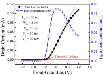
Transconductance is a measure of how fast the transistor is able to switch while sweeping the gate voltage, and it is related to the gain of the transistor. It is given by the ratio of the change in drain current to the change in gate voltage at a constant drain-source bias. The transconductance is a measure of the sensitivity to surface charges [10]. A high transconductance value means a bigger change in drain current for a given change in surface charge which translates to higher device sensitivities. For that reason, the maximum transconductance gate voltage is sometimes chosen as the operating point for sensor measurements. High maximum transconductance values > 10 μS were found for all devices, (Figure 2.6, right axis) [16].
The transconductance is defined as the derivative of Eq. (1.22) with respect to Vgs:
[ ]
(2.28)
The threshold voltage extraction using the linear extrapolation method for a short channel device operated in the linear region as shown in Figure 2.6. The intercept point with X-axis indicates the threshold voltage [17]. The slope of the line yields the mobility. However, this method is sensitive to the mobility degradation and series resistance. The
27
maximum slope of gm usually lies in the non-linear tail of the Id-Vgs curve. Thus, this method tends to obtain a value of Vt closer to the point where Id becomes negligibly small.
Figure 2.6 Experimental drain current and transconductance curves as a function of
front-gate bias showing the linear extrapolation method for threshold voltage. N-channel SOI MOSFET with LG = 100 nm and Tsi = 10 nm [18].
From Eq. 2.24, if μeff is constant, the transconductance gm can be calculated as:
(2.29)
ID increases linearly with Vds.
1.7. Subthreshold slope
One of the most well-known feature of a FET device is the semi-logarithmic plot of the drain current Id as a function of the gate voltage Vgs, called Id(Vgs) transfer characteristic, as illustrated in Figure 2.7 [15].
28
Figure 2.7 log scale (b) of simulation drain current (IDS) versus gate voltage (Vgs) for TG FinFET device [19].
For Vgs < Vth, one can define the subthreshold region, a region of particular interest for sensing applications. An explicit expression for the Id in the subthreshold region for a double-gate thin-film is provided in [20]:
( ) ( ( )( )) [ ( )] [ ]
(2.30)
where µn is the electron mobility, CSi = Si/tSi is the capacitance per unit area associated to the silicon film, Vds and Vgs the voltage at the drain and gate contacts. The variation of the Id current according to Vgs in the subthreshold region is expressed by the subthreshold slope (inverse or the real slope of Id(Vgs)), defined as:
(2.31)
Where is called body m-factor and it describes the coupling between the gate and the
surface potential, while
, known as n-factor, is limited to a minimum value according to the Fermi-Dirac distribution. For a bulk MOSFET the subthreshold slope can further be expressed as:
(
) (
) (2.32)
where CD and Cit are the capacitances associated to the depletion region and the interface trap states, respectively. The subthreshold slope is constant and independent from the drain and
29
gate voltage. An ideal FET device has a subthreshold slope of SS0 = 59 mV/dec at room temperature (300 K) [19]. The full-depletion condition allows thin-film to get closer to the ideal value. In first approximation, the variation of the depletion charge with the front gate is, in fact, δQD/δVgs = 0, meaning that CD ≈ 0 and the subthreshold slope approaches its theoretical limit [21] with m = 1:
(2.33)
which is valid for small thicknesses (tSi < xdmax) [22] and neglecting the interface traps. Under scaling, the subthreshold slope of a thin-film device with the same parameters of a bulk device or thick-film will be steeper. In turns, in the subthreshold regime any variation of gate voltage δVgs is perfectly coupled to the surface potential φS, giving rise to an equal increase. In a real device, the theoretical limit is never reached due to the presence of traps at the Si-Oxide interface.
1.8. Drain induced barrier lowering (DIBL)
DIBL is one of the most important short channel effect parameter of nanoscale FET device structures, since it estimates the overall gate control of the device on the channel electrostatics of the device. The effect of DIBL is to reduce the threshold voltage in nanoscale MOS devices thanks to the modulation of the source to drain channel potential barrier by the drain voltage. This makes the conduction of device channel available for smaller gate voltages [23]. The DIBL is defined as the ratio of the difference in threshold voltage measured at a low value to high value of the drain voltage. The drain induced barrier lowering is defined as the ratio of change in threshold voltage ∆Vth to change in drain voltage ∆Vds [24]. DIBL (mV/V) = DS Th ΔV ΔV (2.34)
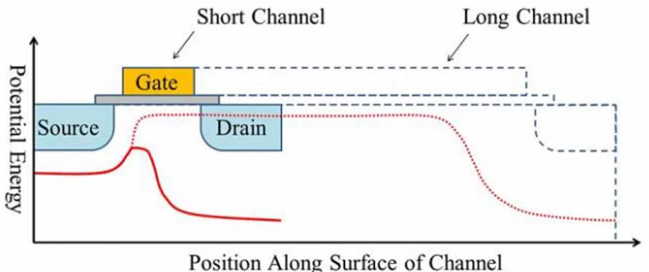
DIBL is more prominent at high drain voltages and shorter channel lengths. We can reduce drain induced barrier lowering effect by using higher surface and channel doping [24, 25]. For a short channel device, VDS lowers the potential barrier between source and channel, which is named drain-induced barrier lowering (DIBL) as shown in Figure 2.8.
30
Figure 2.8 Drain-induced barrier lowering in short channel device. Drain is biased and it
pulls down the potential energy around drain [18].
This effect limits the maximum operation voltage of device [26]. To avoid DIBL, the enhancement of gate control or the separation of merged depletion region is needed. Thus, increase of substrate doping level, delta doping into the substrate and the so-called pocket or halo implant, has been used in typical planar devices [27-28].
31
1.9. Mobility
Carrier mobility is considered as an attractive concept over the years in industry and research. However, mobility and its properties are generally investigated in the context of planar structures and doping levels, crystal quality, electric fields, and temperature [29, 30]. Exciting thesis research topics let the researchers focus on carrier mobility on crystal orientations other than the most frequently used (100)-oriented silicon surface.
Carrier mobility represents how quickly carriers can move in the material. When an electric field E is applied across the material, the carriers acquire a velocity in the field direction. This velocity is superimposed to the random thermal induced motion. An average velocity, named drift velocity v, may be used to describe the ensemble movement of the carriers:
v E (2.35)
where μ is the carrier mobility. In case of very intense electric field the velocity saturates [18];
Each mobility source has different temperature dependences; they can be identified by low temperature measurement. Jeon et al. and Takagi et al. showed the temperature dependence of each scattering mechanism using experimental mobility analysis [31, 32].
2. The Silicon FET as a Nanoelectronic Device 2.1. What is Nanotechnology ?
Nanotechnology has been defined as work at the scale range 1 to 100 nm lengths to produce structures, devices, and systems that have novel properties because of their nanoscale dimensions [33]. Within this nanoscale regime, new phenomena occur (caused, for example, by the dominance of interfaces and quantum mechanical effects). These new phenomena may be exploited to improve the performance of materials, devices, and systems. Nanotechnologies also involve the manipulation and control of matter at the nanoscale. The top-down methods for processing of nanostructured materials involve starting with lithography/etching a bulk solid and then obtaining a nanostructure by structural decomposition. In the current day, silicon technology meets the definition of nanoelectronics very well and that unconventional technologies could play an important role in future electronic system by complementing the capabilities of nanoscale silicon technology, rather than by attempting to replace it [34].
32
2.2. Silicon material
Silicon has formed the basis material of the semiconductor industry, almost since its birth and has remained the material of choice since it superseded germanium, which was used to make the first transistors. Silicon has the advantages of being easily obtainable (comprising a quarter of the Earth’s crust), therefore inexpensive. It has good physical properties that allow easy definition of complex device structures. Lastly its oxide is a very good electrical insulator and, unlike that of germanium, is insoluble in water which reduces processing complexity. These factors combine to provide a cheap platform on which to fabricate reliable FinFETs [8].
It is known that 21st-century silicon technology has evolved into a true nanotechnology which is already below 100 nm. The materials used in these silicon devices have properties very different from that of the bulk materials. Nanoscale silicon transistors have higher leakage current, lower drive current, and exhibit more variability from device to device. New circuits and architectures will need to be developed to accommodate such devices. It matters little whether the material is silicon or something else; the same issues face any nanoelectronics technology. It is likely that many of the advances and breakthroughs at the circuits and systems levels that will be needed to make nanoelectronics successful will come from the silicon design community [34].
The importance of developing and understanding of how engineering devices operate at the nanoscale is a good reason to support nanoscience research. Another reason is that devices to complement silicon technology might be discovered. Therefore, research on nanoelectronics will prove to be a good investment for several reasons [34].
Accelerating the development and successful of nanoelectronics will require a partnership between science and engineering. It was the same for semiconductor technology. The scientific community developed the understanding of semiconductor materials and physics and the engineering community used this base to learn how to design devices, circuits, and systems. Figure 2.9 summarizes this partnership. Science works in the nanoworld with individual atoms, molecules, nanoscale structures and devices, and assembly processes. Systems engineers work in the macroworld on complex systems with terascale device densities [34].
33
In the middle are the device and circuit engineers. This section needs to learn how to think and work at the nanoscale to build devices and circuits that can connect to the macroworld. This job is to hide the complexity of the nanoscale device by packaging it in a form that systems engineers can use (e.g., a compact circuit model). To turn the promise of nanoscience into practical technologies, it is essential that the systems engineering community be engaged in the effort [34].
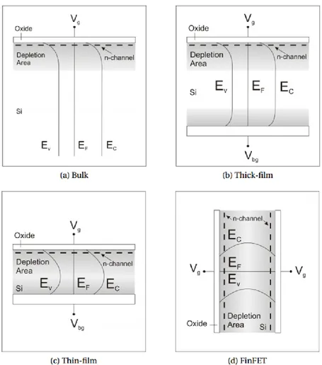
2.3. Silicon FETs in the Nanometer Regime
Nanoscale device technology is a current topic of research for all the production companies, like TSMC, Intel, and Samsung, which are in the race to get a high performance of microprocessors beyond the barrier of 14 nm. The International Technology Roadmap for Semiconductors (ITRS) looking for get 9-nm physical gate lengths for integrated circuit (IC) transistors in 2016 [35]. At the same time, major IC manufacturers have reported transistors with 10-nm (or shorter) gate lengths on IEDM 2002 [36, 37], which demonstrate the promise of pushing IC technology to the 10-nm regime. To scale silicon transistors down to the 10-nm scale, new device structures are needed to suppress the short channel effects such as subthreshold voltage (SS), Drain Induced Barrier Lowering (DIBL), and high leakage current (Ioff) [38]. Figure 2.10 shows a schematic illustration of a fully depleted, double-gate (DG) MOSFET; this device offers good prospects for scaling silicon transistors to their limits [39]. Other approaches (e.g., the FinFET [36] and the tri-gate MOSFET [40]) are also being explored. At a 9-nm gate length, acceptable short-channel effects require a fully depleted
34
silicon body thickness of 3 nm or less, and an equivalent gate oxide thickness of less than 1 nm. At such dimensions, the properties of the silicon material will be affected by quantum confinement (e.g., the bandgap will increase), and device properties will be influenced by quantum transport.
Figure 2.10 The double-gate MOSFET structure [34].
Traditional device equations are based on the drift-diffusion theory [38], which assumes that the device scale is much larger than the electron wavelength (∼ 8 nm at room temperature) and the electron mean free-path (the average distance an electron travels between two collisions, ∼ 10nm for electrons in the inversion layer). The first assumption allows the researchers to treat electrons as classical particles with zero size, and the second one justifies the ―local transport‖ property (the electron velocity at a position is solely determined by the local electric field and mobility). Unfortunately, at the nanoscale, neither of these assumptions is well satisfied. As a result, to capture the new physical effects that occur at the nanoscale, the old device theory must be modified or even completely replaced by a new quantum transport theory. Four important phenomena need to be properly treated in the modelling of nanotransistors [34]:
1. Quantum confinement 2. Gate tunneling
3. Quasi-ballistic transport
4. Source-to-drain (S/D) tunneling
The first two effects occur in the confinement direction (normal to the gate electrode(s)) of the FET device. As silicon technology entered the sub-100-nm regime (the corresponding oxide thickness <3nm), those effects became significant and began to affect
35
the FET device threshold voltage and leakage currents in the ―Off-state‖. In contrast to the quantum confinement and gate tunneling, quasi-ballistic transport, the source-to-drain tunneling begin to significantly affect the device performance of the silicon FET transistor when the gate length scales down to 10 nm or less [41]. Therefore, the exploration of these microscopic transport effects is important for the description of silicon FinFETs at their scaling limit, as well as the understanding of device physics of other nanoscale devices [34].
2.4. The short channel effect
The short channel effect is the decrease of the device threshold voltage as the channel length is reduced. This is important as it is hard to control channel lengths precisely due to process tolerances. Statistical variations in channel lengths then lead to problems with Vth control [42].
Providing the channel is sufficiently long, the source and drain depletion regions only occupy a small fraction of the entire channel and Vgs controls essentially all of the depletion charge. Thus the MOSFET can be abruptly switched off. As the channel length decreases, the fraction of charge controlled by the gate decreases. Less gate charge is now required to invert the channel, resulting in a lower Vth. With increasing Vds, the reverse-biased depletion region at the drain extends further into the channel area and the gate controls even less depletion charge, further lowering Vth. When Vds is sufficiently high or channel length sufficiently short, the drain depletion region merges with the source depletion region. Thus the source-channel potential barrier is lowered below the built in potential resulting in significant drain leakage current with the gate unable to shut it off. Control of the channel by the gate can be retained by not only increasing Cox but by proper scaling down of the source and drain junction depths and scaling up of the substrate doping concentration. Increasing the doping concentration reduces the depletion region widths; however, the carrier mobility is degraded due to increased number of ionized impurities and increased vertical electric field. In addition, Vth is increased. If the source and drain junction depths were equal to the inversion layer thickness, the gate would retain complete control of the channel. Achieving such ultra-shallow junctions is limited by diffusion of the source and drain dopants [8].
2.5. Channel control
The electrostatics of the device channel can be controlled much more effectively by using multiple gates than in the FDSOI MOSFET, allowing for further scaling. The basic principle is shown in Figure 2.11 which shows how the addition of a second gate further
36
suppresses the source and drain depletion regions. This notion has given birth to a host of three-dimensional multi-gate MOSFETs which include a range of double-gate, triple-gate, and surrounding-gate MOSFETs, with the latter theoretically providing the best possible control of the channel region.
2.6. Multi-gate transistors
Various innovative device structures have been proposed by researchers to address the above mentioned challenges and continue device scaling. In these transistors, the channel is surrounded by multiple gates, allowing better control of the channel and thus yielding more effective suppression of leakage current. Multi-gate transistors also have higher on-current (Ion), which leads to better device performance [43]. Among various multi-gate transistors, double-gate field-effect transistors (DGFETs) have gained popularity owing to ease of fabrication and better yield [44]. The presence of the second gate helps a DGFET to reduce drain influence on the channel and thus reduce short-channel effects such as DIBL and degraded subthreshold slope (SS).
Figure 2.11 Cross section of a fully depleted double-gate MOSFET. The electric fields
(arrows) and corresponding depletion charges from both gates and the source and drain are shown [8].
37
Figure 2.12 compares DIBL and SS of a conventional device and a DGFET based on MEDICI (device simulator) predicted data at various effective channel lengths (LEFF) [45]. It can be seen that both the DIBL and subthreshold swing are improved by using the double gate structure. Thus, a DGFET enables scaling to the 22 nm technology node and beyond. Figure 2.13 not only shows reduced off-current (Ioff), but also demonstrates an improved Ion/Ioff ratio.
Figure 2.12 DIBL and subthreshold swing versus effective channel length for DG and bulk-silicon nFETs. The DG device is designed with an undoped body and a near-mid-gap gate
material [45].
Figure 2.13 IDS-VGS characteristics on log scale for DGFETs and bulk-silicon transistors at equalized subthreshold current [45].
38
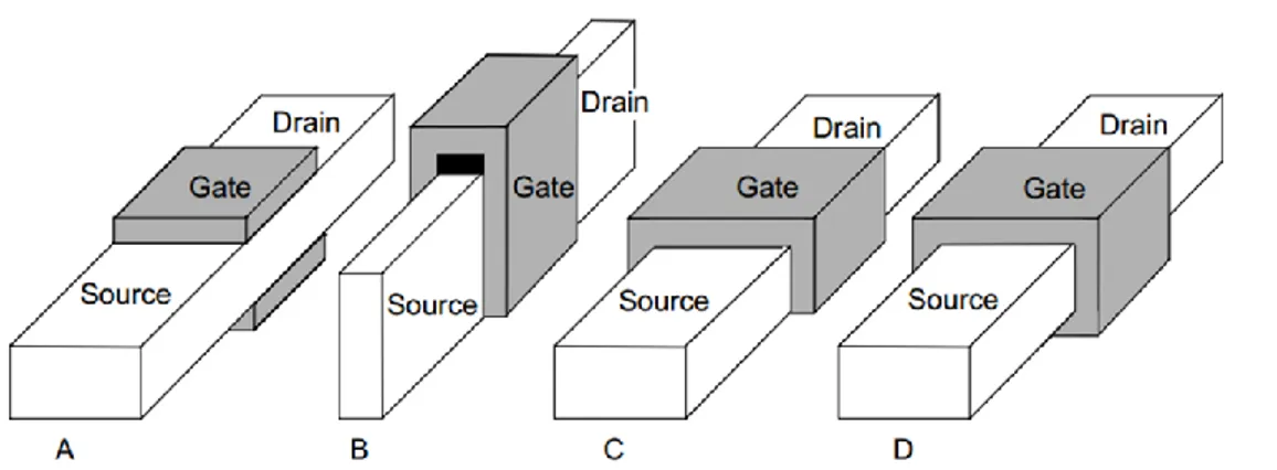
Figure 2.14 shows three major types of DGFETs. Type I augments a conventional FET with a second gate buried in the body itself. In Type II, the silicon body is rotated to a vertical orientation with drain/source sitting at the top/bottom. In Type III, the silicon body is made to stand up with source/drain being on either side of the channel. Type III is popularly known as FinFET. Some major challenges in fabricating DGFETs are maintaining an identical size for both the gates, alignment of the gates, alignment of source/drain to the gates, and connecting both gates in an area-efficient manner. FinFETs address these fabrication concerns and, hence, have emerged as the most promising DGFET [46].
Beyond the tri-gate FinFET, Gate-All-Around (GAA) will be the optimized gate structure in 3D multi gate MOSFETs. GAA FET has gate electrodes wrapped around the channel region. Extremely narrow nanowire channel body has pseudo-1D channel structure. The short channel effect immunity of nanowire FET can be quantitatively analyzed by using natural length λ which can be derived from Poisson’s equation (Table 2.1) [2].
Figure 2.14 Different kinds of DGFETs [46].
39
The natural length is the length of the channel region controlled by the drain. It means that the smaller λ, the smaller short channel effect can be driven in given device structures. To be free of short channel effects, λ should be at least 5 times shorter than the effective gate length. From the equation of λ with single, double, and triple gates, it can be simply guessed that approximately the value of λ can be estimated by division with the square root of gates number. Because the smaller λ can reduce the short channel effects, the device has good immunity from increased gate number. Moreover, from these equations, it should be notable that the reduction of tox decreases short channel effects. Decreasing tox has a limitation due to the tunneling current leakages below 1.5 nm gate oxide thickness. Thus high-k gate dielectric can effectively reduce λ. The effect of tsi thinning is also essential to decrease λ and short channel effects. A quantum confinement induced by tsi reduction enhances the volume inversion effect and yield the increase of Vth. However, ultra-thin body raises the mobility degradation even though the reduction of tsi can decrease short channel effects [47].
2.6.1. FinFETs technology
FinFET has been considered as an attractive candidate for advanced CMOS technology node applications. This nonplanar double-gate transistor has emerged as most viable alternative [2, 45] owing to low subthreshold leakage, superior gate control over the channel, and reduced sensitivity to process variations. Initially, the cost and complexity associated with fabrication were the primary challenges in making these devices the industry driver. These are no longer critical as the key players in the semiconductor industry have
40
managed to fabricate these devices at roughly the same cost and with minor modifications to the conventional CMOS fabrication process. Superior performance, significantly lower leakage, and low fabrication cost are the main reasons behind recent adoption of these devices by various companies. Intel was the first company to introduce FinFET technology into mass production, in 2011, and reported that the manufacturing cost is comparable to that of the conventional planar MOSFET technology, higher by only a low single-digit percent. It also reported that no special manufacturing equipment is required [48]. TSMC has announced availability of 14nm FinFET chips on 450mm wafers by 2016 [49]. Samsung had demonstrated a functional FinFET based SRAM as far back as 2005 [50]. A fully functional chip consisting of 3000 FinFETs was fabricated by Infineon in 2006 [51]. Major industry players like IBM, Globalfoundries, Toshiba, and NEC joined to design the smallest area (0.063 square micron) FinFET based SRAM using optical lithography at the 22 nm technology node [52]. They demonstrated such an operational SRAM at 0.4V. Intel, another semiconductor giant, has taken a different route by introducing a tri-gate FET (a variant of FinFET) at the 22 nm technology node. Intel was the first company to manufacture products, which basically have their applications in computers and servers at the 22 nm tri-gate FinFET technology and currently is looking to grow at a high rate in future with the market of the 7 nm FinFET technology. FinFET is one of the most attractive devices for implementing nanoscale CMOS technology which gives improvement on electrical and physical design convergence at advanced nodes such as the products of CPU, SoC, FPGA, MCU, and network processor. Clearly, all major players in the semiconductor industry have accepted FinFETs as the prime workhorse to continue scaling in the upcoming decade. Hence, our focus in this thesis is to investigate this device in depth, identify potential challenges, and try to address them through novel solutions.
41
A FinFET can have multiple fins in parallel, all straddled by a single gate line, thus its effective width is given by;
Weff = n(2Hfin + Wfin) (2.36)
where n is the number of fins, Hfin and Wfin is the fin height and width respectively. Adequate suppression of the short channel effect and off-state leakage current requires that W fin ~ L/2. It is desirable for Hfin to be as large as possible to maximize Weff, therefore Id. Thus for the 22 nm node and beyond, the FinFET can essentially be treated as a fully depleted double gate device where Id flows predominantly along its sidewall surfaces. Due to their vertical nature, a FinFET’s sidewalls and top surface lie in the (110) and (100) planes respectively when the device is oriented parallel or perpendicular to the wafer flat of a standard (100) wafer. Id therefore flows along the <110> direction. In this orientation, the hole mobility is maximized but the electron mobility is minimized. The electron mobility could be maximized by rotating the fins 45° as then the sidewalls would be in a (100) plane. However this incurs an area penalty on the wafer and increases complexity in circuit design, making it an unlikely option in VLSI circuits.
2.6.2. Silicon on insulator (SOI) technology
The use of SOI material makes the fabrication of multiple gate devices easier. Different kinds of transistors are developed such as: double gate [54], triple gate [55], FinFET [56] or gate all around [57]. Those architectures are summarized on Figure 2.16.
42
Two, three, or four gates are used to control the channel regions, leading to an increase of the electric field induced by the gate. With multiple gates, the transverse electric field (i.e., gate-to-channel electric field) is reinforced compared to lateral electric field (i.e., source-to-drain electric field). The main purpose of these architectures is to:
• Improve the scaling of the transistors (i.e., by limiting DIBL and short channel effects for a given drive current) for gate length below 50 nm
• Achieve levels of performance that are as good as classical planar CMOS devices.
With the improved performances achieved by those multiple gate SOI devices, we can imagine:
1. Having a lower Ioff for a given Vth criterion of a bulk transistor, possibly thanks to its steeper subthreshold swing
2. Having a lower gate tunneling current
3. Having smaller performance variations, with the combination of intrinsic devices and metal gate material
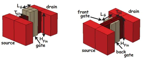
SOI-based FinFETs offer excellent circuit operation due to easier leakage control, better performance, less variability, and lower cost. In an SOI FinFET, a metal gate wraps around an upright thin silicon fin with an insulating base and a thick spacer material at the top that separates the fin from the gate as is shown in Figure 2.16. In tri-gate transistors, the fin can be controlled from all three sides of the device (the top spacer is removed). The use of three gates surrounding the fin ensures an excellent electrostatic control [55]. The smaller fin
Figure 2.16 Scheme of multiple gate SOI devices. Planar double gate (a) FinFET, (b) triple gate,
43
thickness (Tsi) compared to gate length (Lg) ensures tighter control of the channel. The device channel is undoped or lightly doped to eliminate random dopant fluctuations caused by within-die process variations. FinFET functionality follows similar device physics as conventional MOSFETs. The effective width of a FinFET device is 2nHFIN, where n is the number of fins and HFIN is the fin height. The transistor width can be increased to increase Ion by simply adding more fins to the structure (Figure 2.18). However, such a structure leads to width quantization that affects functionality, performance, and power, which are sensitive to the ratio [58].
FinFETs device can be operated in two different modes: SG and IG (Figure 2.19). In the SG mode of operation, the front and back gates are shorted and biased together to switch the device on/off, providing maximum gate drive. In the IG mode of operation, the front and back gates are made independent by etching away the top part of the FinFET, thus, allowing them to be independently biased. This flexibility allows a designer to use a back-gate bias to alter the Vth of the front gate, hence, providing a better way to control Ioff. The back gate of an IG FinFET can be forward (reverse) biased to dynamically increase (decrease) its Ion (Ioff). However, its Ion is still far inferior to the Ion of an SG FinFET [59].
There are two distinct orientations for the Fins: (100) and (110). The channel surfaces of a FinFET lie in the (110) crystallographic plane when the fin is oriented parallel or perpendicular to the wafer flat or notch of a standard (100) wafer. Owing to carrier mobility anisotropy in crystalline silicon [60], the (100) plane maximizes electron mobility, whereas the (110) plane yields maximum hole mobility. This aspect can be exploited to make fast FinFET logic gates. However, as can be seen from Figure 2.18, such a non-systematic fin arrangement results in yield issues for sub-wavelength lithography [61].
44
Figure 2.17 A typical n/p-FinFET device [59]
Figure 2.18 A multiple-fin FinFET structure [59].
![Figure 1.2. Physical structure of an enhancement-type TG n-FinFET transistor [3].](https://thumb-eu.123doks.com/thumbv2/123dokorg/4583908.38823/11.892.262.628.193.576/figure-physical-structure-enhancement-type-tg-finfet-transistor.webp)
![Figure 2.4 I D -V ds characteristics for an n-MOSFET with V G4 >V G3 >V G2 >V G1 >V T [15]](https://thumb-eu.123doks.com/thumbv2/123dokorg/4583908.38823/25.892.157.713.294.972/figure-characteristics-mosfet-gt-g-gt-v-t.webp)
![Table 2.1 Natural length of devices depending on different gate structures [2].](https://thumb-eu.123doks.com/thumbv2/123dokorg/4583908.38823/39.892.227.707.112.389/table-natural-length-devices-depending-different-gate-structures.webp)
![Figure 2.15 FinFET SEM photos. (a) Fabricated FinFET. (b) [53].](https://thumb-eu.123doks.com/thumbv2/123dokorg/4583908.38823/41.892.221.726.116.347/figure-finfet-sem-photos-a-fabricated-finfet-b.webp)