Alma Mater Studiorum
Università degli Studi di Bologna
ARCES – ADVANCED RESEARCH CENTER FOR
ELECTRONIC SYSTEMS
Dottorato di Ricerca in Ingegneria Elettronica
Tecnologie dell’ Informazione
ING-INF/01
Ciclo XX
Memory Hierarchy and Data Communication
in Heterogeneous Reconfigurable SoCs
Tesi di Dottorato di: ARSENIY VITKOVSKIY
Coordinatore Dottorato: Prof. Ing. RICCARDO ROVATTI Relatore: Prof. Ing. ROBERTO GUERRIERI
Corelatore: Dott. Ing. FABIO CAMPI
M
MEEMMOORRYYHHIIEERRAARRCCHHYYAANNDDDDAATTAACCOOMMMMUUNNIICCAATTIIOONNIINNHHEETTEERROOGGEENNEEOOUUSSRREECCOONNFFIIGGUURRAABBLLEESSOOCCSS
ABSTRACT
The miniaturization race in the hardware industry aiming at continuous increasing of transistor density on a die does not bring respective application performance improvements any more. One of the most promising alternatives is to exploit a heterogeneous nature of common applications in hardware. Supported by reconfigurable computation, which has already proved its efficiency in accelerating data intensive applications, this concept promises a breakthrough in contemporary technology development.
Memory organization in such heterogeneous reconfigurable architectures becomes very critical. Two primary aspects introduce a sophisticated trade-off. On the one hand, a memory subsystem should provide well organized distributed data structure and guarantee the required data bandwidth. On the other hand, it should hide the heterogeneous hardware structure from the end-user, in order to support feasible high-level programmability of the system.
This thesis work explores the heterogeneous reconfigurable hardware architectures and presents possible solutions to cope the problem of memory organization and data structure. By the example of the MORPHEUS heterogeneous platform, the discussion follows the complete design cycle, starting from decision making and justification, until hardware realization. Particular emphasis is made on the methods to support high system performance, meet application requirements, and provide a user-friendly programmer interface.
As a result, the research introduces a complete heterogeneous platform enhanced with a hierarchical memory organization, which copes with its task by means of separating computation from communication, providing reconfigurable engines with computation and configuration data, and unification of heterogeneous computational devices using local storage buffers. It is distinguished from the related solutions by distributed data-flow organization, specifically engineered mechanisms to operate with data on local domains, particular communication infrastructure based on Network-on-Chip, and thorough methods to prevent computation and communication stalls. In addition, a novel advanced technique to accelerate memory access was developed and implemented.
M MEEMMOORRYYHHIIEERRAARRCCHHYYAANNDDDDAATTAACCOOMMMMUUNNIICCAATTIIOONNIINNHHEETTEERROOGGEENNEEOOUUSSRREECCOONNFFIIGGUURRAABBLLEESSOOCCSS
KEYWORDS
Reconfigurable architectures Heterogeneous Systems-on-Chip Memory organization Data structureM
MEEMMOORRYYHHIIEERRAARRCCHHYYAANNDDDDAATTAACCOOMMMMUUNNIICCAATTIIOONNIINNHHEETTEERROOGGEENNEEOOUUSSRREECCOONNFFIIGGUURRAABBLLEESSOOCCSS
ACKNOWLEDGEMENTS
This research was sponsored by the European Commission under the 6th Framework program within the MORPHEUS project (IST FP6, project no. 027342). The PhD study was carried out within European Doctorate program in Information Technology (EDITH) at the joint research laboratory of FTM/CCDS STMicroelectronics and Advanced Research Centre for Electronic Systems (ARCES) of the University of Bologna.
I would like to express thanks to my supervisors: Fabio Campi, whose essential guidance and valuable practical advices helped me to increase the scientific quality of my research, and Roberto Guerrieri, who provided me with the continuous support along the whole period of my study. I would also like to thank Georgi Kuzmanov and Georgi Gaydadjiev for the fruitful collaboration during my practical research at CE/EEMCS Delft University of Technology.
M
MEEMMOORRYYHHIIEERRAARRCCHHYYAANNDDDDAATTAACCOOMMMMUUNNIICCAATTIIOONNIINNHHEETTEERROOGGEENNEEOOUUSSRREECCOONNFFIIGGUURRAABBLLEESSOOCCSS
CONTENTS
LIST OF FIGURES ...13
LIST OF TABLES ...15
LIST OF TERMS AND ACRONYMS...17
CHAPTER 1 INTRODUCTION ...21
1.1 MOTIVATION...23
1.2 OBJECTIVES...25
1.3 STATEMENT OF ORIGINALITY...26
1.4 OVERVIEW...27
CHAPTER 2 MEMORY ORGANIZATION IN HETEROGENEOUS RECONFIGURABLE ARCHITECTURES ...29
2.1 STATE-OF-THE-ART RECONFIGURABLE COMPUTING AND RECONFIGURABLE ARCHITECTURES...31
2.1.1 Host integration ...34
2.1.2 Granularity ...35
2.1.3 Heterogeneous architectures ...37
2.2 MEMORY AND COMMUNICATION SUBSYSTEMS IN RECONFIGURABLE ARCHITECTURES...38
2.2.1 The problem of memory sharing in embedded reconfigurable architectures 39 2.2.2 Streaming communication model and automated memory access ...41
2.2.3 Local repository and its implementation trade-offs ...43
2.2.4 Related research on data communication and memory subsystems...44
2.3 SUMMARY...50
CHAPTER 3 OVERVIEW OF THE MORPHEUS HETEROGENEOUS RECONFIGURABLE PLATFORM ...51 3.1 MORPHEUS DESCRIPTION...53 3.1.1 Objectives...53 3.1.2 Target applications ...57 3.2 DESIGN CHALLENGES...61 3.3 HARDWARE ARCHITECTURE...65 3.4 COMMUNICATION INFRASTRUCTURE...68 3.5 DESCRIPTION OF THE IPS...71 3.5.1 PACT XPP ...71 3.5.2 M2000 embedded FPGA...76
10
-3.5.3 PiCoGA ...89
3.6 SUMMARY...108
CHAPTER 4 HIERARCHICAL MEMORY ORGANIZATION AND DISTRIBUTED DATA STRUCTURE ...109
4.1 GENERIC BANDWIDTH REQUIREMENTS...111
4.2 DATA STRUCTURE IN THE SYSTEM...114
4.2.1 Computational data storage...115
4.2.2 Control data storage ...118
4.2.3 Configuration data storage ...119
4.3 MEMORY ARCHITECTURE DEVELOPMENT...123
4.3.1 Level 3: off-chip memory...124
4.3.2 Level 2: on-chip memory...127
4.3.3 Level 1: Data/configuration exchange buffers ...129
4.3.4 Exchange registers ...131
4.4 COMPUTATIONAL MODEL...134
4.4.1 Mathematical representation ...136
4.4.2 Organization of data-flow in the system...137
4.4.3 Network-on-Chip as the data communication mean ...139
4.4.4 KPN modeling ...142
4.4.5 PN modeling...143
4.4.6 Local data synchronizations...145
4.5 HRE INTEGRATION BY THE EXAMPLE OF PICOGA ...151
4.5.1 Integration strategy ...151
4.5.2 Control unit ...154
4.5.3 Address generator ...156
4.5.4 Software tool-chain ...162
4.5.5 Results ...163
4.6 COMPARISON WITH THE RELATED WORK...166
4.7 SUMMARY...170
CHAPTER 5 TWO-DIMENSIONAL PARALLEL MEMORY ACCESS WITH MULTIPLE PATTERN ...173
5.1 INTRODUCTION...175
5.1.1 Research context and goal description...175
5.1.2 Related work...177
5.2 THEORETICAL BASIS...178
5.3 PROPOSED MEMORY ACCESS SCHEME...185
M
MEEMMOORRYYHHIIEERRAARRCCHHYYAANNDDDDAATTAACCOOMMMMUUNNIICCAATTIIOONNIINNHHEETTEERROOGGEENNEEOOUUSSRREECCOONNFFIIGGUURRAABBLLEESSOOCCSS
5.3.2 Row address function ...190
5.3.3 Memory access latencies...190
5.4 DESIGN IMPLEMENTATION AND COMPLEXITY EVALUATION...191
5.4.1 Mode select ...192
5.4.2 Address generator ...193
5.4.3 Row address generator ...195
5.4.4 Module assignment unit ...195
5.4.5 Shuffle unit ...197
5.4.6 De-Shuffle unit ...197
5.5 RESULTS...199
5.5.1 ASIC synthesis...199
5.5.2 FPGA synthesis ...201
5.6 COMPARISON WITH THE RELATED WORK...202
5.7 SUMMARY...205
CHAPTER 6 CONCLUSION ...207
6.1 SCIENTIFIC RESULTS...209
6.2 CONTRIBUTION STATEMENT...210
6.3 FUTURE WORK...211
APPENDIX A. EXAMPLES OF C-SOURCE CODES FOR THE MORPHEUS PLATFORM ...215
APPENDIX B. VHDL SOURCES...221
M
MEEMMOORRYYHHIIEERRAARRCCHHYYAANNDDDDAATTAACCOOMMMMUUNNIICCAATTIIOONNIINNHHEETTEERROOGGEENNEEOOUUSSRREECCOONNFFIIGGUURRAABBLLEESSOOCCSS
LIST OF FIGURES
FIG. 1. SUBSYSTEM AND BANDWIDTH HIERARCHY OF IMAGINE PROCESSOR [28]...46
FIG. 2. BAZIL ARCHITECTURE BLOCK DIAGRAM [72]...46
FIG. 3. ZSP-CORE MEMORY SUBSYSTEM [72]...48
FIG. 4. EPLC-CORE MEMORY SUBSYSTEM [72]. ...48
FIG. 5. BAZIL DATAFLOW [72]...49
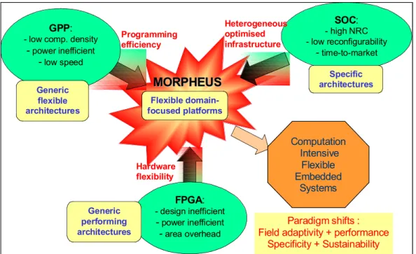
FIG. 6. MORPHEUS OBJECTIVES. ...54
FIG. 7. CONCEPTUAL VIEW OF THE MORPHEUS SOC...61
FIG. 8. MORPHEUS BLOCK DIAGRAM. ...66
FIG. 9. STNOC IMPLEMENTATION OF THE ISO-OSI PROTOCOL LAYERS. ...69
FIG. 10. SPIDERGON TOPOLOGY. ...70
FIG. 11. AN XPP ARRAY WITH 6X5 ALU-PAES...72
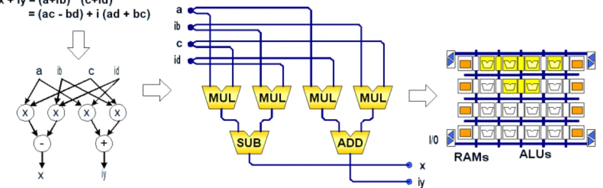
FIG. 12. FLOW-GRAPH OF A COMPLEX MULTIPLICATION AND SPATIAL MAPPING...73
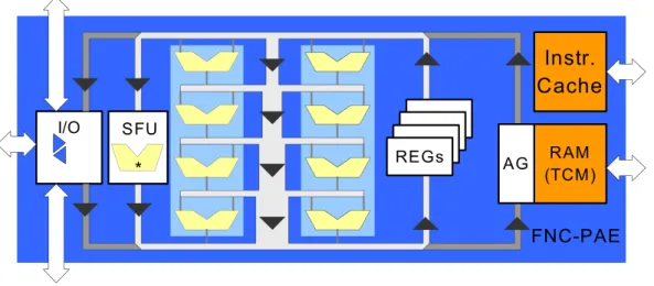
FIG. 13. FNC-PAE BLOCK DIAGRAM. ...75
FIG. 14. FLEXEOS MACRO BLOCK DIAGRAM...77
FIG. 15. MFC SCHEMATIC. ...79
FIG. 16. EMBEDDED DPRAM SCHEMATIC. ...81
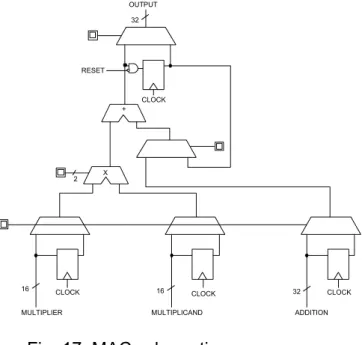
FIG. 17. MAC SCHEMATIC. ...82
FIG. 18. FULL CROSSBAR SWITCH...83
FIG. 19. FLEXEOS CORE ARCHITECTURE. ...83
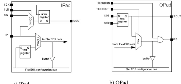
FIG. 20. IPAD AND OPAD CELL WITH SCAN LOGIC...85
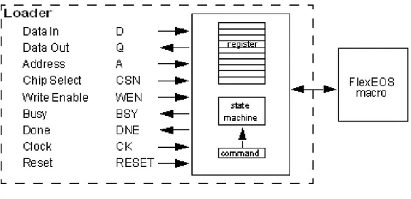
FIG. 21. FLEXEOS LOADER OVERVIEW...86
FIG. 22. FLEXEOS LOADER CONTROL INTERFACE WAVEFORM. ...86
FIG. 23. FLEXEOS SOFTWARE FLOW...89
FIG. 24. SIMPLIFIED PICOGA ACHITECTURE. ...91
FIG. 25. PIPELINED DFG IN PICOGA. ...92
FIG. 26. EXAMPLE OF GRIFFY-C CODE REPRESENTING ASAD (SUM OF ABSOLUTE DIFFERENCES). 94 FIG. 27. EXAMPLE OF PIPELINED DFG. ...94
FIG. 28. EXAMPLE OF PGAOP MAPPING ON PICOGA. ...95
FIG. 29. RECONFIGURABLE LOGIC CELL: SIMPLIFIED ARCHITECTURE...97
FIG. 30. PIPELINE MANAGEMENT USING RCUS. ...99
FIG. 31. BASIC OPERATIONS IN GRIFFY-C. ...100
FIG. 32. SCHEMATIC VIEW ON THE THEORETICAL BANDWIDTH CONSTRAINTS...112
FIG. 33. SIMPLIFIED MORPHEUS ARCHITECTURE. ...115
FIG. 34. MORHEUS SOC ARCHITECTURE. ...117
FIG. 35. CONFIGURATION DATA HIERARCHY...120
FIG. 36. HRE CONFIGURATION...122
14
-FIG. 38. CLOCK DOMAIN DATA STORAGE ORGANIZATION...131
FIG. 39. GENERAL VIEW OF THE DATA-FLOW ON THE MORPHEUS PLATFORM. ...134
FIG. 40. EXAMPLE OF A POSSIBLE DATA FLOW ORGANIZATION ON THE MORPHEUS ARCHITECTURE. ...135
FIG. 41. NOC SPIDERGON TOPOLOGY. ...140
FIG. 42. INITIATOR AND TARGET HRE-NI. ...141
FIG. 43. REPRESENTATION OF THE PING-PONG BUFFERING. ...145
FIG. 44. SYNCHRONIZATION SCHEME. ...146
FIG. 45. ARM C-CODE REPRESENTING HW HANDSHAKE. ...147
FIG. 46. DREAM C-CODE REPRESENTING HW HANDSHAKE...148
FIG. 47. SW SUPPORT FOR THE CONFIGURATION LOAD PROCEDURE...150
FIG. 48. DREAM INTEGRATION. ...152
FIG. 49. EXAMPLE OF THE PROGRAMMING CODE FOR DREAM...155
FIG. 50. INTEGRATION OF THE AG IN DREAM ARCHITECTURE. ...157
FIG. 51. A CLASSIFICATION OF MEMORY ACCESS TYPES ENABLED BY AG...159
FIG. 52. AG BLOCK DIAGRAM. ...162
FIG. 53. THROUGHPUT VS. INTERLEAVING FACTOR. ...164
FIG. 54. SPEED-UP WRT. ARM9 PROCESSOR...165
FIG. 55. PROPOSED MEMORY ACCESS PATTERN. ...178
FIG. 56. PROBLEM PARTITIONING. ...185
FIG. 57. INTEGRATION OF PARALLEL MEMORY CONTROLLER. ...191
FIG. 58. PARALLEL MEMORY CONTROLLER BLOCK DIAGRAM...192
FIG. 59. MODE SELECT BLOCK DIAGRAM...193
FIG. 60. ADDRESS GENERATOR BLOCK DIAGRAM. ...195
FIG. 61. PARALLEL COUNTER BLOCK DIAGRAM...195
FIG. 62. MODULE ASSIGNMENT UNIT BLOCK DIAGRAM. ...196
FIG. 63. SHUFFLE UNIT BLOCK DIAGRAM...197
FIG. 64. DE-SHUFFLE UNIT BLOCK DIAGRAM. ...198
FIG. 65. SYNTHESIS RESULTS FORASIC 90 NM: DESIGN COMPLEXITY, FREQUENCY AND THROUGHPUT...200
M
MEEMMOORRYYHHIIEERRAARRCCHHYYAANNDDDDAATTAACCOOMMMMUUNNIICCAATTIIOONNIINNHHEETTEERROOGGEENNEEOOUUSSRREECCOONNFFIIGGUURRAABBLLEESSOOCCSS
LIST OF TABLES
TABLE 1. EDRAM SIZE AND CONFIGURATION OPTIONS. ...81
TABLE 2. DPRAM INTERFACE SIGNALS...81
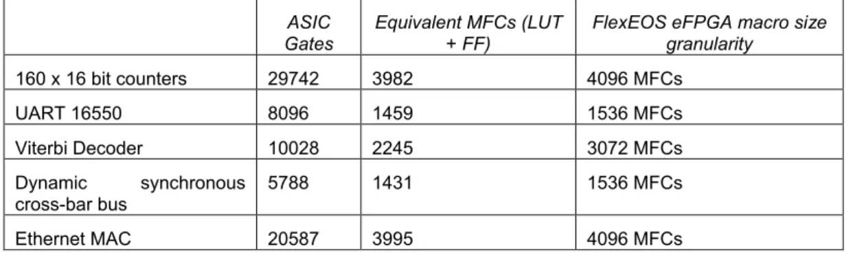
TABLE 3. FLEXEOS 4K-MFC FEATURES AND SIZE. ...87
TABLE 4. EXAMPLE OF DESIGN MAPPING RESULTS...87
TABLE 5. PARAMETER FORMAT FOR PGAOP POSITION SPECIFICATION (BITS). ...104
TABLE 6. NODES ANNOTATION. ...112
TABLE 7. INTER-NODE BANDWIDTH REQUIREMENTS...113
TABLE 8. MEMORY HIERARCHY LEVELS. ...116
TABLE 9. CONFIGURATION BITSTREAM REQUIREMENTS FOR THE MORPHEUS IPS. ...119
TABLE 10. AREA REQUIREMENTS FOR DUAL CLOCK CEBS. ...121
TABLE 11. AN EXTERNAL BANDWIDTH PROVIDED BY A GENERAL PURPOSE MEMORY CONTROLLER. ...126
TABLE 12. STANDARD MEMORY ACCESS...158
TABLE 13. MASKED MEMORY ACCESS. ...159
TABLE 14. AREA OCCUPATION AND ENERGY CONSUMPTION...163
TABLE 15. PERFORMANCE OF SEVERAL APPLICATION KERNELS...164
TABLE 16. MEMORY ACCESS PATTERN PARAMETERS...179
TABLE 17. CORRESPONDENCE TABLE. ...193
TABLE 18. MODULE ASSIGNMENT FUNCTION COMPLEXITY FOR DIFFERENT CASES. ...197
TABLE 19. SUMMARY OF THE TECHNOLOGY INDEPENDENT DESIGN COMPLEXITY EVALUATION. ...199
TABLE 20. SYNTHESIS RESULTS FORASIC 90 NM...200
TABLE 21. FPGA SYNTHESIS RESULTS...201 TABLE 22. COMPARISON TO THE SCHEMES WITH 8 MEMORY MODULES AND 8 BITS DATA WIDTH. .203
M
MEEMMOORRYYHHIIEERRAARRCCHHYYAANNDDDDAATTAACCOOMMMMUUNNIICCAATTIIOONNIINNHHEETTEERROOGGEENNEEOOUUSSRREECCOONNFFIIGGUURRAABBLLEESSOOCCSS
LIST OF TERMS AND ACRONYMS
AG Address Generator
AHB Advanced High-performance Bus
ALU Arithmetical Logic Unit
AMBA Advanced Microcontroller Bus Architecture [1] API Application Programming Interface
ASIC Application Specific Integrated Circuit
CEB Configuration Exchange Buffer
CLB Configurable Logic Block
CPMA Configurable Parallel Memory Architecture
DEB Data Exchange Buffer
DFG Data-Flow Graph
DMA Direct Memory Access
DNA Direct Network Access
DPM Dynamical Power Management
DRAM Dynamic RAM
DSP Digital Signal Processor
DSS Dynamic Storage Scheme
DVFS Dynamic Voltage and Frequency Scaling
eFPGA Embedded FPGA
FFT Fast Fourier Transform
FIFO First In, First Out
FPGA Field Programmable Gate Array
FSM Final State Machine
GCD Greatest Common Divisor
18
-GPP General Purpose Processor
Granularity Refers to the size of the computational data element (see section 2.1.2)
HDL Hardware Description Language
HRE Heterogeneous Reconfigurable Engine
HW Hardware
I/O Input/Output
ILP Instruction Level Parallelism
IP Intellectual Property
ISA Instruction Set Architecture
KPN Khan Process Net
LCM Least Common Multiple
LUT Look-Up Table
MIMD Multiple Instructions, Multiple Data is a technique employed to achieve parallelism.
MPSoC Multi-Processor SoC
MUX Multiplexer
NoC Network-on-Chip
PN Petri Net
QoS Quality of Service
RA Reconfigurable Architecture
RAM Random Access Memory
RC Reconfigurable Computing
RF Register File
RISC Reduced Instruction Set Computer
RTL Register Transfer Level
RTOS Real-Time Operating System
M
MEEMMOORRYYHHIIEERRAARRCCHHYYAANNDDDDAATTAACCOOMMMMUUNNIICCAATTIIOONNIINNHHEETTEERROOGGEENNEEOOUUSSRREECCOONNFFIIGGUURRAABBLLEESSOOCCSS
SIMD Single Instruction, Multiple Data is a technique employed to achieve data level parallelism.
SoC System-on-Chip
SPR Special-Purpose Register
SRAM Static RAM
SRF Stream RF
SW Software
TCM Tightly Coupled Memory
VLIW Very Long Instruction Word
CHAPTER 1
INTRODUCTION
In this chapter, a formal definition of the research goal is presented. The discussion follows the reasons that made the research area to arise and outlines its significance in the modern technology development. In the end, a brief overview of the following chapters is given.
M
MEEMMOORRYYHHIIEERRAARRCCHHYYAANNDDDDAATTAACCOOMMMMUUNNIICCAATTIIOONNIINNHHEETTEERROOGGEENNEEOOUUSSRREECCOONNFFIIGGUURRAABBLLEESSOOCCSS
1.1 MOTIVATION
The primary force that pushes the hardware development sector, enabling to appear new devices with faster speed and higher complexity, is better application performance. For four decades, the Moore’s Law that predicts a doubling of transistor density every 18 months has been providing the necessary conditions to satisfy ever-increasing computation requirements. Unfortunately, nowadays we are reaching the limit when constantly mounting transistor density no longer delivers congruous improvements in application performance. The reasons are known well enough, but a clear alternative solution is not yet available. When increasing the amount of transistors, wire delays and speed-to-memory issues acquire greater side-effects. Aggressive single-core designs unavoidably lead to greater complexity and larger power consumption. On top of it all, scalar processors suffer from a fundamental limitation: their design is based on serial execution, which makes it almost impossible to extract more instruction-level parallelism (ILP) from applications.
By now, there are outlined new strategies to supplement Moore's law and, exploring innovative architectures and design concepts, to overcome the limitations of conventional systems. These strategies include:
Multicore systems that use a set of cores of the similar type on a die to continue delivering steady performance gains.
Special-purpose processors, including application specific and reconfigurable architectures, that provide enhanced performance in areas where conventional processors perform much poorly.
Heterogeneous architectures, where computational engines of various nature, complexity and programming approach work cooperatively.
Each of these strategies has potential to deliver substantial performance improvements. However, on the long term, heterogeneous computing has prodigious means for accelerating applications beyond what Moore's law can offer [64], in the same time getting over many of the obstacles that limit conventional architectures. Thus, it is expected for heterogeneous architectures to become extremely important over the next several years.
C
CHHAAPPTTEERR11..IINNTTRROODDUUCCTTIIOONN
24
-Although heterogeneous systems have great potential to obtain significant performance, they might be totally ignored by programmers unless they are able to make use of heterogeneous specifics in applications relatively easy. This requires not only dedicated software environment, but – what is even more important – thoroughly implemented data structure in the system. Heterogeneous architectures may incorporate data-flows of various natures inside the system, such as computation data, configuration data, control data, different synchronization signals, I/O communications and many others, depending on the type and amount of devices integrated into the system. Managing all these flows within a single organization may become a nightmare. The data structure is primarily based on the interconnection strategy inside the system as well as data storage allocation. Communication and memory subsystems are responsible for the efficient traffic routing, fast and timely data access, and prevention of computational stalls induced by bottle-neck(s) in communication interface(s). Such interfaces are very design critical, being able to introduce great benefits, if enhanced with specific mechanisms to provide the amount and kind of data specifically required by the running application. Thus, intelligent distribution of the data-flows in the system supported by communication and storage means can provide clear programming model for the user. Because of the predefined and well regulated interaction between computational engines, a number of application mapping stages can be easily automated by the compiler or other software tools. In the aggregate, all described above mechanisms enable not only stable system functionality, but also lighten programmer’s effort of mapping complex applications.
M
MEEMMOORRYYHHIIEERRAARRCCHHYYAANNDDDDAATTAACCOOMMMMUUNNIICCAATTIIOONNIINNHHEETTEERROOGGEENNEEOOUUSSRREECCOONNFFIIGGUURRAABBLLEESSOOCCSS
1.2 OBJECTIVES
This research targets complex reconfigurable Systems-on-Chip with heterogeneous organization. Such systems unify computational engines of various natures, such as general-purpose, application specific, reconfigurable and other devices, within a common architecture. In order to benefit from running complex applications, the integrated engines feature different computational densities and purposes. Application mapping for such systems becomes a very sophisticated task, requiring much manpower and time resources.
The objective of this research is to develop a memory organization that would hide the heterogeneous nature of the system from the programmer, providing a user-friendly interface for application mapping. From the user point of view, the system should represent as close as possible a conventional single-processor architecture with distributed storage organization. Such systems exploit the traditional programming model, thus having the advantage of a clear and well-understood concept of application mapping.
Simultaneously, this approach should preserve the inherent advantages of the reconfigurable architectures that are primarily designed for data intensive computations. Therefore, it is important to provide the required data bandwidth to these devices, supporting respective parallelization and run-time adjustability of the memory access according to the target application needs. In this scope, it is prerequisite to optimize the memory access in order to provide the required data-flow for the most data-hungry computational engines.
C
CHHAAPPTTEERR11..IINNTTRROODDUUCCTTIIOONN
26
-1.3 STATEMENT OF ORIGINALITY
Correct organization of the memory subsystem as well as data structure is the crucial task in heterogeneous reconfigurable architectures. However, this context emerged quite recently and thus, generalized methodologies and solutions are not yet state-of-the-art. This research aims at exploring novel approaches and trade-offs to extend the huge opportunities of heterogeneous architectures to the memory infrastructure.
In this scope, topical matter relates to a memory access optimization. Automated addressing FSMs have been successfully used for a long time with high-end Digital Signal Processors (DSPs). However, it is an open research field for massively parallel systems based on GPPs and FPGAs of various natures [10].
M
MEEMMOORRYYHHIIEERRAARRCCHHYYAANNDDDDAATTAACCOOMMMMUUNNIICCAATTIIOONNIINNHHEETTEERROOGGEENNEEOOUUSSRREECCOONNFFIIGGUURRAABBLLEESSOOCCSS
1.4 OVERVIEW
The thesis structure is organized as follows. Chapter 2 presents a retrospective of the reconfigurable computing and specifics of the heterogeneous nature of hardware architectures. The main stress is put on the memory subsystem and its significance in the context of the whole system performance. The basic terms, concepts, notions and definitions are given.
Chapter 3 introduces the MORPHEUS target architecture, making emphasis on the most relevant concepts of this research.
Chapter 4 describes the exploration on memory organization and its detailed implementation in the context of the target system.
Chapter 5 discusses the further enhancements of the research topic, presenting the advanced parallel memory access acceleration technique. Together with the previous chapter, this one presents numerical results and comparison with the related works.
Finally, Chapter 6 concludes the thesis by summarizing the developed techniques and solutions, outlining the contribution of this work in the scope of the total project, and showing questions arose by this research that can be basement for the future work.
CHAPTER 2
MEMORY ORGANIZATION IN HETEROGENEOUS
RECONFIGURABLE ARCHITECTURES
This chapter presents backgrounds and related research in the area of heterogeneous reconfigurable architectures. The special emphasis is done on the role which memory subsystem plays in the target hardware architectures. Simultaneously, a number of important definitions and general concepts are given which will appear throughout the entire work. All along the discussion, the references to the related work are provided in order to complete a picture of the state-of-the-art research and development in the target area.
M
MEEMMOORRYYHHIIEERRAARRCCHHYYAANNDDDDAATTAACCOOMMMMUUNNIICCAATTIIOONNIINNHHEETTEERROOGGEENNEEOOUUSSRREECCOONNFFIIGGUURRAABBLLEESSOOCCSS
2.1 STATE-OF-THE-ART RECONFIGURABLE COMPUTING AND
RECONFIGURABLE ARCHITECTURES
Because of its capability to significantly speed-up a large variety of applications, reconfigurable computing has become a subject of a large amount of research. Its most important feature is the ability to run computations in hardware with high performance, while keeping a lot of the flexibility peculiar to software solutions.
Traditionally in computing, there are two primary methods for the execution of algorithms. The first method is to use purely hardware technology, either an Application Specific Integrated Circuit (ASIC) or a group of individual components (or Intellectual Properties, IPs) integrated in a complex system. ASICs are designed targeting specific computational task. Therefore, they are very efficient when executing the exact computation they were designed for. However, after fabrication the device cannot be adjusted if any part of it requires further improvement, and complete circuit is forced to be redesigned and refabricated. This is an expensive process in terms of resources and time-to-market, especially considering the difficulties imposed by replacing ASICs in a big amount of deployed systems.
The second method is to use software-programmed microprocessors, which is a much more flexible solution. In order to perform a computation, processors operate on a specific Instruction Set Architecture (ISA), peculiar to the processor architecture. Execution of different instructions from the ISA alters the system functionality without changing its hardware. However, this method has its own drawback, which consists in significant performance degradation because of low clock speed and/or work rate, being far below that of an ASIC. The processor reads every instruction from memory, decodes it, and only after that executes it. This brings about a large execution overhead for each individual operation. Pipelined organization of the instruction execution can reduce the latency overhead by means of additional circuit complexity, and thus higher power consumption, but is not capable to eliminate it completely. In addition, the ISA is defined at the fabrication time of the processor. Any other operations that are to be implemented must be built out of existing instructions.
C
CHHAAPPTTEERR22..MMEEMMOORRYYOORRGGAANNIIZZAATTIIOONNIINNHHEETTEERROOGGEENNEEOOUUSSRREECCOONNFFIIGGUURRAABBLLEEAARRCCHHIITTEECCTTUURREESS
32
-Reconfigurable computing (RC) in its turn fills the gap between hardware and software solutions, offering potentially much higher performance than software-programmable architectures, while keeping a higher level of flexibility than hardware technologies. Reconfigurable devices, organized in the form of Field-Programmable Gate Arrays (FPGAs), consist on an array of computational elements whose functionality is specified by multiple programmable configuration bits, called configuration bitstream. These elements are interconnected by means of a set of programmable routing resources. Thanks to such organization, custom digital circuits, composed by a set of logic functions, can be mapped to the reconfigurable hardware by computing the these functions within the computational elements, and using the programmable routing resources to connect the elements together in order to form the necessary circuit.
RC has been shown to accelerate a variety of applications. Taking as example a set of software kernels for multimedia applications, DREAM reconfigurable processor [21] shows average performance about 30 GOPS and 1.8 GOPS/mm2. For comparison, an ARM926EJ-S processor [9] in the same technology node achieves the performance up to 0.5 GOPS and 0.32 GOPS/mm2. Neglecting some minor overheads, it would thus be necessary to provide up to 60 ordinary processors to match the performance delivered by DREAM on computation intensive kernels.
In order to achieve such performance supporting a wide range of applications, reconfigurable systems are usually organized as a combination of reconfigurable logic and a General-Purpose Processor (GPP). The processor performs various data-dependent control operations that cannot be done efficiently in the reconfigurable logic, while the computation intensive cores are mapped to the reconfigurable hardware. This reconfigurable logic is usually composed of either commercial FPGAs or custom configurable hardware.
Compilation environments for Reconfigurable Architecture (RA) range from tools to assist a programmer in performing a hand mapping of an appropriate functionality to the hardware, to automated systems that map circuit functionality, described in a high-level language, to a reconfigurable system. The design process involves a number of stages. First, a program is partitioned into blocks to be
M
MEEMMOORRYYHHIIEERRAARRCCHHYYAANNDDDDAATTAACCOOMMMMUUNNIICCAATTIIOONNIINNHHEETTEERROOGGEENNEEOOUUSSRREECCOONNFFIIGGUURRAABBLLEESSOOCCSS
implemented on hardware, and those which are to be implemented in software on the host processor. The computations intend for the reconfigurable hardware are synthesized into a gate level or register transfer level (RTL) circuit description. This circuit is mapped onto the computational elements within the reconfigurable hardware which are connected using the reconfigurable routing. After compilation, the circuit is ready for configuration onto the hardware at run-time. These steps, when performed using an automatic compilation environment, require relatively small effort, whereas, performing these operations by hand can result in a more optimized circuit for performance-critical applications.
However, the efficiency of the mapping depends not only on the carefully developed manual task distribution or on the advance of automated tools, but also it depends – to a certain extant, even more – on the exact architecture of the target reconfigurable system, its data structure and memory access facilities. This problem acquires even more significance when the matter concerns complex systems unifying two or more reconfigurable devices. Intensive data traffic between reconfigurable units, memory and main processor faces the prospects of communication bottle-necks and computation stalls. In order to avoid such problems, reconfigurable system should represent clearly organized architecture, transparent for compilation tools and end-user.
Since FPGAs are forced to pay an area penalty because of their reconfiguration capability, device capacity can sometimes be a concern. Systems that are configured only at power-up are capable to elaborate only as much of functionality as will fit within their programmable structures. In order to accelerate additional program sections, the reconfigurable hardware should be reused during program execution. This process is known as run-time (or dynamical) reconfiguration (RTR). While this concept allows for the acceleration of a greater portion of an application, it also introduces the configuration overhead, which limits the amount of acceleration possible. Methods such as configuration compression and the partial configuration can be used to reduce this overhead.
Consideration must be given to a fact that reconfigurable computing is very young and rapidly developing concept. Its classifications are still being
C
CHHAAPPTTEERR22..MMEEMMOORRYYOORRGGAANNIIZZAATTIIOONNIINNHHEETTEERROOGGEENNEEOOUUSSRREECCOONNFFIIGGUURRAABBLLEEAARRCCHHIITTEECCTTUURREESS
34
-formed and refined as new architectures are developed. No unifying taxonomy has been suggested to date. However, several inherent parameters can be used to classify these systems.
2.1.1 HOST INTEGRATION
Host integration is often encountered in practice, when the reconfigurable hardware is coupled with a GPP. The reason is that programmable logic tends to be inefficient at implementing certain kinds of operations, such as variable-length loop and branch control. In order to increase the efficiency, the program sections that cannot be sufficiently mapped to the reconfigurable logic are executed on a host processor. Whereas, the sections with a high computation density, that can benefit from implementation in hardware, are mapped to the reconfigurable logic. For the systems that use a GPP in combination with reconfigurable logic, there are several methods to couple these two computation structures.
1. Reconfigurable hardware may be implemented solely to provide reconfigurable capabilities within a host processor [61], [40]. This solution provides a traditional programming environment with the addition of custom instructions that may vary over time. The reconfigurable units operate as functional units on the main processor data-path using registers to hold the input and output operands.
2. A reconfigurable unit can be used as a coprocessor [80], [54], [63], [20], [8]. In general, a coprocessor is larger and more independent than a functional unit, being able to perform computations without the constant supervision of the host processor. After initialization phase of the reconfigurable hardware, the processor either sends the necessary data to the logic, or provides an address in the memory where this data might be found. The reconfigurable unit performs the necessary computations independently, and returns the results after completion. Such integration strategy allows the reconfigurable unit to operate for a large number of cycles without interfering from the host processor, and potentially permits the host processor and the reconfigurable logic to operate in parallel. This, in its turn, decreases the overhead induced by the use of the reconfigurable logic, compared to the first approach when the reconfigurable unit
M
MEEMMOORRYYHHIIEERRAARRCCHHYYAANNDDDDAATTAACCOOMMMMUUNNIICCAATTIIOONNIINNHHEETTEERROOGGEENNEEOOUUSSRREECCOONNFFIIGGUURRAABBLLEESSOOCCSS
communicates with the host processor each time a reconfigurable instruction is used.
3. An integrated reconfigurable unit [78], [7], [39] behaves as if it is another processor in a multiprocessor system or an additional computation device accessed through external I/O. The data cache of the host processor is not visible to the attached reconfigurable hardware. Therefore, there is longer communication latency between the reconfigurable unit and the host processor or main memory. This communication is performed though specific primitives similar to multiprocessor systems. In spite of the latency drawback, this type of RA allows for a great deal of computation independence, by shifting large segments of a computation over to the reconfigurable unit.
All of the described organizations target various communication and computation models. The tighter the integration of the reconfigurable unit, the more frequent is its computation/control data exchange with the host system due to a lower communication overhead. However, tightly coupled hardware is unable to operate with more or less significant segments of data without intervention from a host processor, and the amount of available reconfigurable resources is often quite limited. The more loosely coupled solutions allow for greater execution parallelism, but suffer from higher communications overhead.
2.1.2 GRANULARITY
Reconfigurable hardware is assembled from a set of similar computation elements that form a matrix. These basic elements, traditionally called Configurable Logic Blocks (CLBs), features various complexity from a simple block that can perform computation on a bit-level with few inputs (usually, up to three), to a structure operating on a word-level, organized as a small Arithmetical Logic Unit (ALU). The size and complexity of the basic CLBs is referred to as the block’s (or RA’s) granularity.
An example of a fine-grained RA is the Xilinx6200 series of FPGAs [6]. Its functional unit can implement two- or three-input functions. Although such architecture is efficient for bit manipulations, it can be too fine-grained to rationally implement a number of circuits, such as multipliers. Similarly, finite
C
CHHAAPPTTEERR22..MMEEMMOORRYYOORRGGAANNIIZZAATTIIOONNIINNHHEETTEERROOGGEENNEEOOUUSSRREECCOONNFFIIGGUURRAABBLLEEAARRCCHHIITTEECCTTUURREESS
36
-state machines (FSMs) frequently are too complex to be reasonably mapped on fine-grained logic blocks.
Other RAs use a granularity of logic block that can be referred as medium-grained [41], [42], [46]. For instance, Garp [41] was designed to perform a set of operations on up to four 2-bit inputs. Another medium-grained structure is embedded inside a general-purpose FPGA to implement multipliers of an adaptive bit width [42]. The CLB used in this architecture is capable of mapping a 4 x 4 multiplication, or being cascaded into bigger structures. The CHESS architecture [46] also operates on 4-bit inputs, with each of its CLBs acting as a 4-bit ALU. In general, medium-grained architecture may be utilized to implement data-path circuits of varying widths, which makes it more similar to the fine-grained structures. However, having the possibility to perform more complex operations of a greater number of values, medium-grained structure can be efficiently used for a wider range of operations.
Coarse-grained architectures are mainly used for the implementation of word-width data-path circuits. Since their CLBs are optimized for large computations, they perform these operations much faster and consume fewer resources than a set of smaller elements connected together to form similar structure. However, because of their fixed internal architecture, it is impossible to make optimizations in the size of operands. The RaPiD [35] and the Chameleon [3] architectures are examples of this which are composed of word-sized adders, multipliers, and registers. If, e.g., only three 1-bit values are required to process, the efficiency of these architectures suffers from a redundant area and speed overhead, since the computation is performed on all of the bits in the full word size.
The granularity of the RA also implies a significant effect on the reconfiguration time of the device. This is a noticeable issue for run-time reconfiguration, when the length of the reconfiguration phase influences the performance of the complete system, causing computation stalls and communication traffic jams. A fine-grained array requires many configuration points to perform very small computations, and thus requires longer bitstream during configuration.
M
MEEMMOORRYYHHIIEERRAARRCCHHYYAANNDDDDAATTAACCOOMMMMUUNNIICCAATTIIOONNIINNHHEETTEERROOGGEENNEEOOUUSSRREECCOONNFFIIGGUURRAABBLLEESSOOCCSS
Thus, the granularity parameter effects not only the internal RA functionality, such as efficient computation mapping, execution speed, resource occupation, and power consumption; but also it influences the host system performance in terms of computational efficiency and data distribution. This problem can be solved by having both coarse- and fine-grained arrays and on the same chip.
2.1.3 HETEROGENEOUS ARCHITECTURES
In order to achieve greater performance and computation flexibility, the RAs of mixed granularity can be integrated together within a common system. Such systems are called heterogeneous because they unify hardware of various complexity and computational capability.
The most relevant advantage of the heterogeneous approach is that it potentially allows each integrated device to perform the tasks to which it is best suited. This model can employ the dedicated RAs to accelerate some operations up to 100 times faster than what conventional processors can achieve, and consequently expanding the applicability of conventional processor architectures. In the situation when applications include both code segments that could benefit from acceleration and code segments that are better suited for conventional processing, there is no single type of processor which would equally satisfy computation strategies. Heterogeneous organization makes it possible to map each operation of a given application on the right hardware type.
However, there are two primary obstacles hampering heterogeneous RA to be widespread [64]: the programming complexity required for efficient distribution of workloads across multiple computational engines, and the additional effort, required to map a code segment on the appropriate computational device, induced by a specificity of its hardware architectures. These issues can impose significant difficulties, so that any possible advantage of a heterogeneous approach should be compared with the costs to overcome them.
C
CHHAAPPTTEERR22..MMEEMMOORRYYOORRGGAANNIIZZAATTIIOONNIINNHHEETTEERROOGGEENNEEOOUUSSRREECCOONNFFIIGGUURRAABBLLEEAARRCCHHIITTEECCTTUURREESS
38
-2.2 MEMORY AND COMMUNICATION SUBSYSTEMS IN
RECONFIGURABLE ARCHITECTURES
For a long time, the integration of RA in embedded systems has been considered a very attractive alternative for the pure Application Specific Integrated Circuits (ASICs). It allows obtaining software level programmability having the performance of conventional ASICs. The increasing performance and the usability of RA make them a feasible solution for computationally intensive tasks, thus guaranteeing the required data bandwidth for the RA becomes the key implementation issue.
Typically, the software programmable architectures have sequential organization, i.e. a small set of data is computed at a time (usually two, a few more for VLIW or superscalar processors). In these architectures, a HW computational unit is strictly separated from a memory region, providing flexible and programmable addressing mechanism based on single random access. Such architectures also feature a local register file (RF) and a memory access pattern, so that addressing of computation data is performed by specific instructions. Compilers support this addressing mechanism, decomposing the data patterns in terms of collections of single load/store operations, which are described by control flow statements (e.g. for/while loops). The high sophistication degree of modern compilation techniques and the appropriate skillfulness in high level programming languages allow covering almost all kinds of regular data addressing patterns required by applications.
Another feature of ASIC is its space-oriented computation where a theoretically infinite number of computation operands may be required for any given operation. Therefore, data transfer organization in an ASIC is not a trivial task, and it is crucial for its performance. On the other hand, it is always possible to implicitly remove programmability and to implement any data flow and operand retrieving pattern as a part of the design itself. Temporary storage resources, which are usually distributed between computational units and dedicated data channels, are specifically designed where it is required.
In order to benefit from natural parallelism of RA, it is essential to provide a data bandwidth comparable to that of ASICs. In addition, to justify their
M
MEEMMOORRYYHHIIEERRAARRCCHHYYAANNDDDDAATTAACCOOMMMMUUNNIICCAATTIIOONNIINNHHEETTEERROOGGEENNEEOOUUSSRREECCOONNFFIIGGUURRAABBLLEESSOOCCSS
integration in a given embedded system, RAs need to be capable of changing the addressing pattern in order to match the reconfigurable computation. Therefore, one of the most critical parts of the system architecture is to assure a suitable data structure which would feed with data such computation dense core. Thus, the bottleneck is passed on to the rapidly growing requirements of the respective memory infrastructure. Thoroughly designed memory subsystem, organized in a layered manner with multi-port local buffers, programmable DMA, efficiently implemented main memory controller and intelligently distributed temporal storage repository, become mandatory. Pure off-chip solutions, without essential on-chip aids, lack the required bandwidth and are unacceptable regarding power consumption and system costs. Memory architecture in reconfigurable SoCs poses additional challenges to the digital designer, since target applications often require flexible memory access patterns (e.g. various word sizes, parallel access or different addressing modes).
2.2.1 THE PROBLEM OF MEMORY SHARING IN EMBEDDED RECONFIGURABLE ARCHITECTURES
In the beginning of the era of reconfigurable architectures, the first designs were oriented at extending the instruction set of standard RISC processors. Machines like PRISM [15], PRISC [61], OneChip [80] in a way or another all used reconfigurable hardware to extend the processor computation capabilities, while still relying on the processor for handling memory accesses.
As the reconfigurable computing development leads to the design of more and more dense extension blocks, these blocks also become more data hungry. One issue that rose from this efforts is that the function unit paradigm, although elegant and compiler friendly, hardly provides enough computation parallelism to justify the reconfigurable hardware utilization. Following proposals in the area of reconfigurable architectures showed a specific interest on the data feeding mechanism. XiRisc [22], if similar in many aspects to the cited designs, provides a three-way VLIW configuration to enhance memory access bandwidth. Garp [20] presents a specific data addressing mechanism implemented in the reconfigurable array. The Molen programming paradigm and HW architecture [74] distributes data in the system in two ways:
C
CHHAAPPTTEERR22..MMEEMMOORRYYOORRGGAANNIIZZAATTIIOONNIINNHHEETTEERROOGGEENNEEOOUUSSRREECCOONNFFIIGGUURRAABBLLEEAARRCCHHIITTEECCTTUURREESS
40
- Small amounts of data are exchanged between the processor core and the reconfigurable unit through specific Exchange Registers (XRs).
Intensive data streams can be connected directly to the extension unit, but in this case either the data flow is routed to the unit with a streaming pattern, or the unit itself is provided with a HDL coding that specifies the type of addressing required
In this case, the user is required to design the addressing pattern of the extension instruction as part of the computation design, as it is the case for ASIC implementation. This solution has the relevant advantage of minimizing exchanges between the unit and the external memory hierarchy, as temporary variables can be handled locally. On the other hand, the approach of mapping memory addressing as part of the micro-coded extension segments could be costly in terms of resources and will make any kind of co-compilation impossible creating two different and separate compilation domains. Also, this solution can only be valid for fine grained reconfigurable units such as embedded FPGAs, while it is hardly applicable to coarse-grained logics. An example of embedded reconfigurable processor where memory access patterns are implemented on the eFPGA fabric is described in [18].
With respect to all architectures mentioned above, coarse grained reconfigurable fabrics feature a significantly different computational grain of the ISA extension segments. As a consequence of this shift, connection between reconfigurable units and the system memory in order to provide enough data to exploit the extension segment potential appears as even more severe. Most coarse-grained data-paths such as Pact XPP [77] or PipeRench [39] do not actively intervene on the data layout: they simply consume data streams, provided by standard external sources or appropriately formatted by an external processor core or by specific DMA logic. Morphosys [66] is only slightly more sophisticated, featuring a dedicated frame buffer in order to overlap data computation and transfers over orthogonal chunks of variable width.
Another interesting solution is the ADRES architecture [51]. ADRES exploits a reconfigurable unit that is similar to that of Morphosys, based on coarse-grain processing elements. In contrast to Morphosys, the ADRES
M
MEEMMOORRYYHHIIEERRAARRCCHHYYAANNDDDDAATTAACCOOMMMMUUNNIICCAATTIIOONNIINNHHEETTEERROOGGEENNEEOOUUSSRREECCOONNFFIIGGUURRAABBLLEESSOOCCSS
reconfigurable hardware is used as a functional unit in the frame of a VLIW processor. Data exchange with external memory is realized through the default path of the VLIW processor, and data exchanges take place on the main register file, as it was the case for XiRisc. The programming model is thus simplified because both processor and reconfigurable unit share the same memory access. ADRES is completed by a compilation environment [50] that schedules Instruction Set Architecture (ISA) extensions in order to exploit maximum concurrency with the VLIW core and handles data addressing towards the VLIW register file for both reconfigurable array and hardwired core. A relevant additional value of the compiler, that made the RF-oriented micro-architecture, is that extension instructions are generated by the same compilation flow that produces code for the hardwired core. The provided data is thus randomly accessed and it is not limited to data streaming. However, the VLIW register file may remain a bottleneck for intensive data-flow. A different solution is provided by Montium [67], a coarse-grain reconfigurable processor composed of a scalable set of Tile Processors (TP). Each TP is equiped with RAM buffers, feeding each ALU input. Buffers are driven by a configurable automated Address Generation Unit (AGU). Montium is affected by the same bottleneck as most of architectures overviewed above: in order to exploit its computational density, it needs to fetch from a data repository several operands per clock, and possibly each of them featuring an independent, if regular, addressing pattern.
2.2.2 STREAMING COMMUNICATION MODEL AND AUTOMATED MEMORY ACCESS
In conventional multi-processor embedded systems with high level of computational parallelism, data throughput becomes a significant issue on the path to achieving the expected performance and exploiting the available computational power. State-of-the-art DSP architectures, and massively parallel FPGA devices have dealt extensively with such problems.
A general solution is to structure communication between data storage and processing units in a streaming way. The memory subsystem is based on configurable stream units that move data while computation is performed. Stream units are specialized addressing and data communication blocks that are optimized
C
CHHAAPPTTEERR22..MMEEMMOORRYYOORRGGAANNIIZZAATTIIOONNIINNHHEETTEERROOGGEENNEEOOUUSSRREECCOONNFFIIGGUURRAABBLLEEAARRCCHHIITTEECCTTUURREESS
42
-for contiguous data transfers. They are organized as a set of stream descriptors, which define the memory access pattern, to pre-fetch and align data in the order required by the computational block. By utilizing the stream units in the memory subsystem, the architecture effectively decouples communication from computation and allows dealing with their implementation and optimization individually [14]. The stream units benefit from pre-fetching data before it is needed and, consequently, the system performance becomes dependent on the average bandwidth of the memory subsystem with less sensitivity to peak latency to access a data element. Chai S.M. et al [25] outline the following main properties of streaming computation model:
Software computation kernels are independent and self contained. They are localized in such a way that there are no data dependencies between other kernels. The user annotates portions of a program that exhibit this behavior for mapping onto a stream processor or accelerator.
Computation kernels are relatively static. The processing of each computation kernel is regular or repetitive, which often comes in the shape of a loop structure. There are opportunities for compiler to optimization the computation and the access patterns.
Explicit definition of communication. Computation kernels produce an output data stream from one or more input streams. This stream is identified explicitly as a variable in a communication data-flow or a signal between computation kernels.
Data movement completely controlled by programmer. A programmer can explicitly define data transfer from memory to other computation kernels. Hardware mechanisms, such as a DMA or stream unit, provide this capability without intercepting the main processor. The stream communication model allows either minimization of data movement by localizing the computation, or pipeline of computation with data movement. If memory bottlenecks arise, the programmer can retune the memory access.
Automated address generation based on regular patterns can be considered a promising option for providing high performance reconfigurable hardware with
M
MEEMMOORRYYHHIIEERRAARRCCHHYYAANNDDDDAATTAACCOOMMMMUUNNIICCAATTIIOONNIINNHHEETTEERROOGGEENNEEOOUUSSRREECCOONNFFIIGGUURRAABBLLEESSOOCCSS
the required bandwidth. In fact, embedded applications, and especially those that benefit most from mapping on reconfigurable architectures, typically feature kernels based on regular addressing patterns, where addressing is more often is generated and incremented with regularity as part of a loop. A convenient way to retrieve data at high parallelism, commonly used in state of the art highly parallel DSPs, is to utilize programmable stridden addressing generation FSMs.
This is achieved in Morpheus by making use of programmable Address Generators (AG), that are appropriately set at the beginning of each computation kernel, and will produce a new local address at each clock or, more precisely, at each request from the data-path, depending on the issue delay of the required computation. Automated addressing FSMs thus add a new level of configurability to the system, providing an adaptive addressing mechanism for reconfigurable units, thus greatly enhancing their potential exploitation of inherent parallelism. As it is the case with reconfigurable computing in general, automated addressing can be considered a viable alternative only if supported in the long term by solid compilation tools that could spare the end user from manual programming. In fact, it is possible to automatically extract from a high level specification of the algorithm (typically C/C++) regular addressing patterns to be applied to automated addressing FSM.
2.2.3 LOCAL REPOSITORY AND ITS IMPLEMENTATION TRADE-OFFS
On-chip static memories (SRAMs) tend to become slower when the variability effect is present [79]. The bigger the design margins that have to be added in the design with negative implications in meeting specific performance constraints, the slower is the actual performance of the system. This effect becomes more evident at higher frequencies, where not only more power is being consumed, but also the slack between the required performance and the one offered by the memories becomes tighter at every technology node. To address this problem, it is necessary to relax operating frequency while still meeting the application real time constraints. One of the advantages of reconfigurable computing is that frequency requirements can be relaxed utilizing parallel architectures for both the functional units and the local layer of the memory hierarchy [53]. For this reason, it is useful to define a memory layer local to the
C
CHHAAPPTTEERR22..MMEEMMOORRYYOORRGGAANNIIZZAATTIIOONNIINNHHEETTEERROOGGEENNEEOOUUSSRREECCOONNFFIIGGUURRAABBLLEEAARRCCHHIITTEECCTTUURREESS
44
-RA, which can be addressed as a single item by the system, but is organized in small local banks that can be accessed concurrently by all ports of the reconfigurable unit.
The physical structure of such banks can organized as a traditional MUXed SRAM. Built around a standard, off-the-shelf memory manufactured in high volume, a MUXed SRAM offers a very attractive cost structure in terms of power, area and timing. However, this advantage might be misleading: although a standard MUXed SRAM costs less than a specialized dual-port memory on a per-bit basis, the total cost from a system perspective might be significantly higher. Any architecture with shared memory access built around a standard RAM device will require additional facilities in order to enable access to a common memory block for two computational units. This will require additional design resources and most likely will elongate the development cycle. Furthermore, after layout stage, the additional logic may occupy a physical area comparable to that of integrated dual-port memory while requiring additional place and route cost. Considering the performance implications, it appears that a single port MUXed SRAM suffers from a severe disadvantage relative to a multi-port alternative. Since the single port has always to be switched from one device to another, each device accessing the MUXed SRAM will be limited to less than half of the maximum theoretical bandwidth. On the other hand, a multi-port memory capable of supporting simultaneous access, often across different bus widths and frequencies, imposing no delay on either port during a read or write operation. Consequently, its maximum performance will exceed the traditional MUXed SRAM by a factor of at least two [16]. While the technological density is continuously increasing, it is important to move the performance closer to its theoretical capability, narrowing the gap between HW density and practical functionality.
2.2.4 RELATED RESEARCH ON DATA COMMUNICATION AND MEMORY SUBSYSTEMS
There is a number of streaming processor architectures presented in literature over recent years. We can mark out several examples: RAW [73], IMAGINE [28], Merrimac [29], and the RSVP™ architecture [27], [48]. A set of
M
MEEMMOORRYYHHIIEERRAARRCCHHYYAANNDDDDAATTAACCOOMMMMUUNNIICCAATTIIOONNIINNHHEETTEERROOGGEENNEEOOUUSSRREECCOONNFFIIGGUURRAABBLLEESSOOCCSS
computational models supporting streaming concept, such as SCORE [24], ASC [52], and Streams-C [38] was also developed.
The IMAGINE processor represents a programmable architecture that achieves the performance of special purpose hardware on graphics and image/signal processing. This is realized by exploiting stream-based computation at the application, compiler, and architectural levels. IMAGINE supports 48 ALUs organized as 8 SIMD clusters. Each cluster contains 6 ALUs, several local register files, and executes completely static VLIW instructions. The stream register file (SRF) is the basement for data transfers on the processor. The memory system, arithmetic clusters, host interface, microcontroller, and network interface all interact by transferring streams to and from the SRF. IMAGINE is programmed at two levels, kernel-level and stream-level. Kernels may access local variables, read input streams, and write output streams, but may not make arbitrary memory references, whereas at the stream-level supported by Stream-C basic functions are provided for manipulating streams and for passing streams between kernel functions. All memory references are deployed utilizing stream load/store instructions that transfer entire streams between memory and SRF. This stream load/store concept is similar to the scalar load/store RISC architecture; it simplifies programming and optimizes the memory system for stream throughput, rather than the throughput of individual accesses. The memory system provides 2.1GB/s of bandwidth to off-chip SDRAM storage via four independent 32-bit wide SDRAM banks operating at 143MHz. The system can perform two simultaneous stream memory transfers. To support these parallel transfers, four streams (two index streams and two data streams) connect the memory system to the SRF. IMAGINE addressing modes support sequential, constant stride, indexed (scatter/gather), and bit-reversed accesses on a record-by-record basis (see Fig. 1).
C
CHHAAPPTTEERR22..MMEEMMOORRYYOORRGGAANNIIZZAATTIIOONNIINNHHEETTEERROOGGEENNEEOOUUSSRREECCOONNFFIIGGUURRAABBLLEEAARRCCHHIITTEECCTTUURREESS
46
-Fig. 1. Subsystem and bandwidth hierarchy of IMAGINE processor [28]. Along with homogeneous stream multi-processor platforms there exists a number of heterogeneous reconfigurable systems, whose memory organization provides different trade-off solutions between computation power and flexibility: examples are Chameleon [3], BAZIL [72], Pleiades [81], etc.
Fig. 2. BAZIL architecture block diagram [72].
The BAZIL architecture is based on the concept of intra-chip DSP and programmable logic block co-processing. Key blocks in BAZIL are LSI Logic ZSP400 (ZSP) and ePLC cores, which are integrated together with other peripherals for external memory and data access. BAZIL's heterogeneous
M
MEEMMOORRYYHHIIEERRAARRCCHHYYAANNDDDDAATTAACCOOMMMMUUNNIICCAATTIIOONNIINNHHEETTEERROOGGEENNEEOOUUSSRREECCOONNFFIIGGUURRAABBLLEESSOOCCSS
architecture can be controlled by bus masters, which include the ZSP and DMA controller, and AHB-bridge. These alternative methods of on-chip cores and peripherals control allow robust solution for system programming. BAZIL supports combined boolean and DSP processing through a flexible core interconnect scheme. There are two types of inter-core communication supported in BAZIL architecture:
An AMBA High-speed Bus (AHB) provides an arbitrated mean for inter-core communication.
The DSP and ePLC blocks are additionally interconnected through a higher bandwidth inter-core interface (DSU) that allows higher throughput and data sharing between cores.
Since BAZIL interfaces are AMBA based, they represent straightforward and convenient concept. The ZSP400 Core exploits in parallel two independent interfaces for memory and peripherals (see Fig. 3): an Internal Port interface for close coupled, single cycle program and data memory; and an External Port for Instruction Unit (IU) and Data Unit (DU) alternative access to external memory and peripherals. Both internal and external ports contain instruction and data interfaces that support either single-port or dual-port memories. The ePLC sub-systems (see Fig. 4) are intended as loosely coupled co-processors for algorithm acceleration. Each ePLC is made up of:
The Multi Scale Array (MSA), containing user programmable portions of the ePLC and consisting of an array of configurable ALU (CALU) Cells. The Application Circuit Interface (ACI), providing the signal interface
between the MSA and the application circuitry.
The PLC Adapter, loading the ePLC configuration data and interfaces to test circuitry, clock and reset control through a Configuration Test Interface. It allows the ePLC programming to be handled over the on chip AHB from flash or other external memory.
C
CHHAAPPTTEERR22..MMEEMMOORRYYOORRGGAANNIIZZAATTIIOONNIINNHHEETTEERROOGGEENNEEOOUUSSRREECCOONNFFIIGGUURRAABBLLEEAARRCCHHIITTEECCTTUURREESS
48
-Fig. 3. ZSP-core memory subsystem [72].
Fig. 4. ePLC-core memory subsystem [72].
In typical broadband processing (see Fig. 5), data is transmitted in a batch or streaming mode through a high-bandwidth buffered interface (PCI port). The data buffer simplifies the caching mechanism of the on-chip data bursts. ePLC blocks are used to perform a range of pre-processing and data reduction operations. Then data is passed to the ZSP, either through shared memory or directly from the DSU for DSP operation. The DSP output data can be either exported off chip or to the ePLC for further post processing via the shared ZSP internal memory. While the DSU does not provide a communication channel between the ePLC subsystems, the ePLC bocks can communicate via the shared ZSP internal memory or FEB. It is also possible to move data between ePLC systems via ZSP controlled AHB traffic. The amount of data available and used in different processing steps (pre-DSP and post-processing) typically is reduced with
M
MEEMMOORRYYHHIIEERRAARRCCHHYYAANNDDDDAATTAACCOOMMMMUUNNIICCAATTIIOONNIINNHHEETTEERROOGGEENNEEOOUUSSRREECCOONNFFIIGGUURRAABBLLEESSOOCCSS
each step. As a result, interfaces required for export of processed data (Ethernet) can have significantly lower bandwidth than those needed during import stages (i.e. PCI).
C
CHHAAPPTTEERR22..MMEEMMOORRYYOORRGGAANNIIZZAATTIIOONNIINNHHEETTEERROOGGEENNEEOOUUSSRREECCOONNFFIIGGUURRAABBLLEEAARRCCHHIITTEECCTTUURREESS
50
-2.3 SUMMARY
To date, reconfigurable computation reached high level of development and proved its feasibility in a great range of implemented devices. Target applications become more and more complex, including dense computation for multimedia kernels, data intensive flows for communication tasks and support for Run-Time Operating Systems (RTOS). Heterogeneous architectures are meant to deal with such applications.
One of the most tricky and critical tasks in heterogeneous hardware design is to well organize the memory susbsystem. In contrast to homogeneous systems, the memory storage of a heterogeneous architecture must deal with data traffic of various nature, granularities and densities. Moreover, it is essential to delimit computational engines from each other in order to fully exploit particular features of each hardware component. In this scope, management of the local storages acquires an additional importance.
There are various methods to provide computational engines with the required data dandwidth. Streaming data-flow, parallel memory access, local data buffering, programmable data pattern – all of them aim at a more efficient and flexible data distribution. Comprehensive utilization of these techniques will allow releasing the full potential of heterogeneous reconfigurable architectures.
CHAPTER 3
OVERVIEW OF THE MORPHEUS HETEROGENEOUS
RECONFIGURABLE PLATFORM
Most of the research was performed in the framework of the MORPHEUS project, which includes an architecture design and hardware development of the heterogeneous reconfigurable platform. Since the project is an integration of the standard blocks, custom-design IPs and conceptual innovations from various industrial and academic partners, it is essential to make a general overview of these contributions and summarize the related to this research features. Consequently, this chapter presents the most relevant features of the MORPHEUS platform which are significant in the scope of the research area of this thesis. Namely, the overview of the platform is detailed with the descriptions of the reconfigurable engines provided by MORPHEUS partners. The presented specifics will be used in the following chapters as a basis for the design concepts’ development and justification.
![Fig. 3. ZSP-core memory subsystem [72].](https://thumb-eu.123doks.com/thumbv2/123dokorg/8229056.128655/48.892.256.596.135.642/fig-zsp-core-memory-subsystem.webp)
![Fig. 5. BAZIL dataflow [72].](https://thumb-eu.123doks.com/thumbv2/123dokorg/8229056.128655/49.892.272.673.227.515/fig-bazil-dataflow.webp)