Journal of Instrumentation
OPEN ACCESS
P-Type Silicon Strip Sensors for the new CMS
Tracker at HL-LHC
To cite this article: W. Adam et al 2017 JINST 12 P06018
View the article online for updates and enhancements.
Related content
Silicon sensor developments for the CMS Tracker upgrade
A Dierlamm
-Planar pixel sensors for the ATLAS upgrade: beam tests results
J Weingarten, S Altenheiner, M Beimforde et al.
-T-CAD analysis of electric fields in n-in-p silicon strip detectors in dependence on the p-stop pattern and doping concentration
M. Printz
-2017 JINST 12 P06018
Published by IOP Publishing for Sissa Medialab
Received: March 13, 2017 Revised: May 18, 2017 Accepted: June 12, 2017 Published: June 27, 2017
P-Type Silicon Strip Sensors for the new CMS Tracker at
HL-LHC
The Tracker Group of the CMS Collaboration
E-mail: [email protected]
Abstract: The upgrade of the LHC to the High-Luminosity LHC (HL-LHC) is expected to increase the LHC design luminosity by an order of magnitude. This will require silicon tracking detectors with a significantly higher radiation hardness. The CMS Tracker Collaboration has conducted an irradiation and measurement campaign to identify suitable silicon sensor materials and strip designs for the future outer tracker at the CMS experiment. Based on these results, the collaboration has chosen to use n-in-p type silicon sensors and focus further investigations on the optimization of that sensor type.
This paper describes the main measurement results and conclusions that motivated this decision. Keywords: Particle tracking detectors (Solid-state detectors); Radiation-hard detectors; Detector modelling and simulations II (electric fields, charge transport, multiplication and induction, pulse formation, electron emission, etc)
2017 JINST 12 P06018
Contents1 Introduction 1
2 Samples and irradiations 2
3 Initial characterization 5
3.1 Electrical characterization 5
3.2 Charge collection and noise 5
4 Performance after irradiation 6
4.1 Electrical characterization 6
4.2 Charge collection and noise 9
5 Simulation of electric fields 14
6 Conclusion 16
Tracker group of the CMS collaboration 20
1 Introduction
The LHC is foreseen to be upgraded to the High-Luminosity LHC (HL-LHC), which will provide an instantaneous luminosity of up to 5–7.5·1034cm−2s−1for an integrated luminosity of 3000 fb−1[1,2]
(up to 4000 fb−1, if the ultimate instantaneous luminosity can be achieved). This increase in
luminosity will require silicon trackers with a significantly higher granularity and radiation hardness
compared to the existing ones [3]. The current CMS Tracker consists of 200 m2of p-in-n type (p-type
strip implants in n-type bulk) silicon strip sensors. The strip pitches range from 80 µm to 205 µm,
the strip lengths from 10 cm to 20 cm and the maximum expected fluence is 1.8 × 10¹⁴n
eq/cm2[4].
The future CMS outer tracker will extend from a radius of 20 cm to 110 cm around the beam pipe. It will utilize silicon strip sensors with 90 µm pitch and a strip length of 5 cm (at radii larger than 60 cm) and for the inner region (at radii between 20 cm and 60 cm) a similar strip sensor with 100 µm pitch and a strip length of 2.5 cm as well as a macro-pixel sensors with a pitch of 100 µm and a pixel length of 1.5 mm. The macro-pixels in the inner layers are motivated by the requirement for higher granularity and better pointing resolution in the Z-direction (along the beam pipe) for
standalone tracks in the outer tracker. The total active silicon area will sum up to about 190 m2. As
illustrated in figure1, the fluence equivalent to the damage caused by 1 MeV neutrons is estimated to
reach about 1.1 × 10¹⁵n
eq/cm2at the inner radius of the outer tracker (corresponding to 3000 fb−1).
The expected total ionizing dose ranges from 10 kGy to 750 kGy [3]. The range of particles that
the detectors will be exposed to consists of charged particles and neutral particles with a ratio of
2017 JINST 12 P06018
Figure 1. FLUKA simulation of the fluence levels in the CMS Tracker after 3000 fb−1[5]. The Z-coordinate
in the legend refers to the distance from the interaction point along the beam line.
formation in silicon depends on the particle type and energy. In addition, ionizing radiation due
to charged particles increases the oxide charge density of the silicon dioxide [7–10], which affects
the surface properties of the strip sensors. Therefore, an irradiation and measurement campaign including (mixed) irradiations with both neutrons and protons (both low and high energy protons were used) was performed, for which results have been published in PhD theses and conference
reports [11–21]. A general description of the campaign, the used materials, results from diode
measurements (IV, CV, TCT), strip sensor characterizations and annealing studies will be reported in a future publication.
This paper presents results derived from measurements using small prototype strip sensors
(table1), including those that illustrate the performance of irradiated p-in-n and n-in-p sensor types,
and motivates the conclusion that n-in-p type sensors are most appropriate for use in the CMS Tracker Phase II Upgrade. The results referred to in this paper are described in several of the aforementioned publications and therefore only the most relevant ones, on which the decision is based on, are summarized for the first time.
2 Samples and irradiations
The AC coupled strip sensors used in this study were processed by one single vendor (Hamamatsu Photonics K.K. (HPK)) on several wafer types with the same mask set. This approach allowed
2017 JINST 12 P06018
Table 1. Layout and process details of the two studied miniature strip sensors. Due to space limitations the
strip lengths are not the same as for the final design.
Parameter Value
Strip length 3.27/2.57 cm
Strip width 19 µm
Strip pitch 80 µm
Strip metal width 31 µm
No. of strips 256 / 64
No. of guard rings 1
Overall dimensions 3.5 cm × 2.3 cm / 2.8 cm × 1.3 cm
Coupling dielectric thickness 300 nm (SiO2/Si3N4)
Strip doping conc. (peak) ∼1 × 1019cm−3
p-stop doping conc. (peak) ∼5 × 1015cm−3
p-spray doping conc. (peak) ∼1 × 1015cm−3
a direct comparison of the properties of the base materials without the additional influence of manufacturing techniques and quality levels employed by different vendors. The details of the sensor
layouts are listed in table1. The sensor types discussed in this paper are n-in-p (highly n-doped
strips in p-doped bulk) sensors with p-stop or p-spray strip isolation as well as p-in-n sensors [22].
Sensors of n-in-n type have not been considered as the associated costs are expected to be much higher and the required double-sided process is more prone to damage of the sensitive backside. The charge collection is expected to be equal to the charge collection of n-in-p type sensors, since the same charge carriers are collected. The sensors are processed on wafers of different thicknesses: thinned wafers made from float-zone silicon (FZ) with a physical and active thickness of 200 µm
and deep-diffused FZ wafers (ddFZ) [23] with a physical thickness of 320 µm and a nominal active
thickness of 300 µm or 200 µm. The active thickness (low doping concentration) for these ddFZ wafers is reduced from the physical thickness of 320 µm by a long-term thermal treatment allowing the high backside doping to diffuse deep into the bulk. One reason for using 200 µm thin sensors is to reduce the material of the tracker (less conversions and multiple-scattering). In addition, thin sensors have a higher average electric field at the maximum operation voltage of 600 V compared to thicker sensors and therefore reduce the drift time (and trapping probability after irradiation). The resistivity of the base material is greater than 3 kΩ cm leading to an initial full depletion voltage below 300 V.
After initial characterization, the sensors were first exposed to reactor neutron irradiations or proton irradiations and in a second step irradiation with the other particle type was carried out
resulting in a mixed irradiation scenario (according to table2). The fluences were chosen such that
the mixed fluences represent approximately the situation at the innermost radii for the two sensor types plus a safety factor of 30% (7 × 10¹⁴neq/cm2for strip sensors at 60 cm and 1.5 × 10¹⁵neq/cm2
for macro-pixel sensors at 20 cm). The fluences for individual particles were selected in such a way that one could interpolate the behavior for protons and neutrons independently and then also compare the two. The selection was limited by the number of available samples and time constraints. For most of the materials and fluence points one sensor was measured.
2017 JINST 12 P06018
Table 2. Overview of irradiations. The listed values approximate the expected conditions in the detector
during operation. Samples are measured after irradiation with one particle type, and after irradiation with the other particle type measurements for several annealing durations follow. Higher mixed fluence represents
a location closer to the interaction point, where charged particles dominate. A fluence of 1.5 × 10¹⁵n
eq/cm2
corresponds to a radius in the tracker of about 20 cm (innermost radius) and 7 × 10¹⁴neq/cm2 to 60 cm
(transition between macro-pixel and strip sensor modules) after 3000 fb−1plus safety factor of about 30 %.
Total Fluence/ Proton Neutron
1014neq/cm2 fraction fraction 3 1 0 4 0 1 5 0 1 7 0.43 0.57 10 1 0 10 0 1 15 0.67 0.33 15 1 0
Although the particle type with the highest flux in the CMS tracker are charged pions of about
500 MeV [24,25] this particle type is not easily available for irradiation tests. The particle type
with displacement damage very similar to these pions are high energy protons [26], which were
considered as the reference particle type for charged hadron damage in this study. Low energy protons are used for comparison and to extend the amount of test points, since they are most easily accessible.
The samples were characterized after the first irradiation step and a short annealing of about
10 minutes at 60◦C (equivalent to approximately two days at 20◦C according to the scaling of
the leakage current as given by [27]) to equalize different annealing conditions during irradiation
and transport. After the second irradiation the samples were characterized after each of several consecutive annealing steps in order to study the change of properties with time at room temperature. This information can be used to define the temperature during maintenance periods and possibly exploit beneficial changes at room temperature.
In addition, low (23 MeV) and high (24 GeV) energy protons were used to study the influence
on defect generation [18]. No significant difference in charge collection (see section4.2) and noise
was observed.
The neutron irradiation was performed at the TRIGA Mark II reactor [28] at
Josef-Stefan-Institute, Ljubljana, Slovenia. The fluences were reached within 5 minutes1at about 40◦C followed
by a 30 minutes period at 30◦C in the irradiation channel for deactivation. The GeV proton
irradiation at the proton synchrotron (PS) [30], CERN, Switzerland, took one to three days at 25◦C.
The MeV proton irradiation at the Karlsruhe Compact Cyclotron (KAZ) [31], ZAG, Germany,
took less than an hour at around −30◦C. All samples were stored in a freezer below −5◦C after
irradiation to prevent further annealing.
2017 JINST 12 P06018
3 Initial characterization
After production and dicing, the samples were characterized before irradiation in terms of static electrical sensor parameters, charge collection and noise performance.
3.1 Electrical characterization
Initially, all sensors were electrically characterized in a probe station. The following measurements were performed:
Total leakage current. The current on the bias line is measured versus bias voltage (IV) with
floating guard ring. Good sensors shall not exceed 2 nA/mm3.
Total capacitance. The capacitance of the sensor is measured versus bias voltage (IV) with floating
guard ring to extract the full depletion voltage.
Strip leakage currents. The leakage current of individual strips are measured to check the
unifor-mity.
Coupling capacitance. The capacitance between strip implant and metal strip is measured at
100 Hz. The capacitance shall be larger than 1.2 pF/(cm × µm).
Current through the dielectric. The current is measured between strip implant and metal strip
applying 10 V. The current shall be smaller than 1 nA.
Bias resistance. The bias resistor at each strip is evaluated by measuring the current when applying
2 V on the DC pad. A resistance between 1.2 and 1.8 MΩ is envisaged.
Interstrip capacitance. The capacitance between neighboring metal strips is measured at 1 MHz
and should be below 1 pF/cm.
Interstrip resistance. The resistance between two strip implants is evaluated by measuring the IV
characteristic from −1 V to 1 V. The resistance should be about ten times higher than the bias resistance; before irradiation even larger than 10 GΩ cm.
An overview of these results can be found in [32]. Within these initial measurements no significant
difference in the properties of n-in-p and p-in-n sensors was observed.
3.2 Charge collection and noise
The charge collection and the noise of the sensors were measured using the ALiBaVa system [33]
based on the Beetle chip [34] and a Sr-90 source. A picture of such a setup is shown in figure2. The
noise is defined as the RMS of the signal per channel taken with random triggers. Internal calibration pulses provide the gain to translate ADC counts into charge in electrons with an uncertainty of about
10% [35]. A noise of 900 e−per channel is measured with the Beetle chip for these sensors. This
noise figure is in the order of magnitude expected for a system operated with the CBC read-out
chip [36] developed for the future CMS strip sensor modules. The noise measured here does not
exactly reflect the noise of the final modules in the upgraded CMS tracker, but still relative noise changes can be used to characterize the impact of different layouts or irradiation levels.
For charge collection measurements, the data acquisition is triggered by a scintillator plus photomultiplier tube placed below the sensor. Clusters are identified by finding channels (seed
2017 JINST 12 P06018
Figure 2. The measurement setup at KIT based on the ALiBaVa system.
strips) with a signal that exceeds five times their noise. Then, neighboring channels with a signal above two times their noise are associated with the same cluster. An example of the cluster charge
distribution is given in figure3. The most probable value (MPV) of the convoluted Landau-Gauss
fit is at 15 700 e−, which translates to 74.8 e−/µm given the active thickness of about 210 µm for
this sensor type as derived from CV measurements. The usage of a Sr-90 source together with one scintillator adds a minor fraction of low energetic electrons to the spectrum increasing the average deposited energy by only about 2%. Within the stated uncertainty of the calibration pulse this
measurement is still compatible with about 75.3 e−/µm as expected from [37] for βγ > 100. For
300 µm thick sensors a cluster charge of 22 500 e−is expected.
The charge collection study is focused on evaluating the seed signal only, since the CBC works in binary mode. The analog input signal will be fed into a programmable comparator for each individual channel without any clustering algorithm. Therefore the single strip charge (here that means the seed signal) has to exceed the threshold set in the readout chip for full efficiency. The average cluster width is about 1.5 to 2 strips and the seed signal is about 80% to 90% of the cluster signal before irradiation.
4 Performance after irradiation
4.1 Electrical characterization
After irradiation the sensors were again characterized electrically in probe stations at −20◦C, which
is the approximate temperature during operation in the CMS detector. Strip parameters, IV and
2017 JINST 12 P06018
Cluster charge / e-0 10 20 30 40 50 60 70 80 90 100 3 10 × Entries 0 100 200 300 400 500 600 700 800 900 ALiBaVa systemNon-irrad. n-in-p strip sensor Bias voltage: 150V
Temperature: +20°C
Figure 3. Cluster charge distribution for a non-irradiated n-in-p type sensor with 210 µm active thickness at
150 V bias voltage and a temperature of 20◦C. The red line is a convoluted Landau-Gauss fit. The data were
acquired with an ALiBaVa system as described in the text.
currents are reproduced in figures4and5. Except for the expected increase in leakage currents
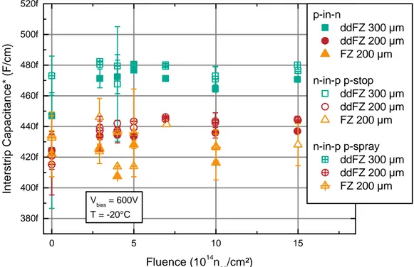
(total as well as for individual strips), the expected tendency of increasing full depletion voltage after possible type inversion and a reduction of the interstrip resistance, no significant changes were observed. Most notably, the interstrip capacitance, which is a big contribution to the noise, did not
change much as shown in figure6. Looking at the post-irradiation data one can see a tendency that
the values for n-in-p type sensors are slightly higher, but still within the errors, which could lead
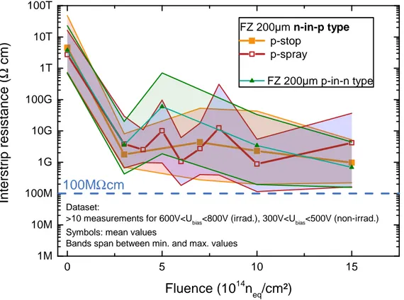
to a small noise increase of up to 3%. The interstrip resistance2dropped from larger than 1 TΩ cm
to between 1 GΩ cm and 10 GΩ cm (figure7). For correct operation of the sensors, the interstrip
resistance should be at least 10 times larger than the resistance of the bias resistors (∼2 MΩ). That would require an interstrip resistance of 20 MΩ. The final sensors will have 5 cm long strips. As test criterion for sensors of different length a minimum of 100 MΩ cm is required. On average this value is exceeded by a large margin with even the lowest measurements lying above this value.
Figure7also shows that there is no significant difference between the isolation techniques. Both
p-stop and p-spray techniques as processed by HPK fulfill the requirements. This means that it is possible to produce n-in-p sensors with sufficient strip isolation which can withstand fluences of up
to 1.5 × 10¹⁵n
eq/cm2, using either isolation technique. This is also demonstrated by simulations
in [38]. It should be pointed out that a careful selection of process parameters is necessary to
ensure the interstrip resistances demonstrated by the samples. A very low p-stop concentration leads to a low interstrip resistance and therefore to a short-circuit of the strips resulting in large
2017 JINST 12 P06018
0 5 1 0 1 5 0 1 0 0 2 0 0 3 0 0 4 0 0 5 0 0 6 0 0 7 0 0 8 0 0 9 0 0 1 0 0 0 1 2 0 0 p - i n - n d d F Z 3 0 0 µ m d d F Z 2 0 0 µ m F Z 2 0 0 µ m M C z 2 0 0 µ m n - i n - p p - s t o p d d F Z 3 0 0 µ m d d F Z 2 0 0 µ m F Z 2 0 0 µ m M C z 2 0 0 µ m n - i n - p p - s p r a y d d F Z 3 0 0 µ m d d F Z 2 0 0 µ m F Z 2 0 0 µ m M C z 2 0 0 µ m D e p le ti o n v o lt a g e ( V ) F l u e n c e ( 1 0 1 4n e q/ c m ² ) > 1 0 0 0Figure 4. Full depletion voltages of strip sensors as extracted from CV measurements [32]. Measurements
on non-irradiated samples were performed at room temperature, else at −20◦C.
0 5 1 0 1 5 0 . 0 0 0 . 0 2 0 . 0 4 0 . 0 6 0 . 0 8 0 . 1 0 0 . 1 2 0 . 1 4 p - i n - n d d F Z 3 0 0 µ m d d F Z 2 0 0 µ m F Z 2 0 0 µ m M C z 2 0 0 µ m n - i n - p p - s t o p d d F Z 3 0 0 µ m d d F Z 2 0 0 µ m F Z 2 0 0 µ m M C z 2 0 0 µ m n - i n - p p - s p r a y d d F Z 3 0 0 µ m d d F Z 2 0 0 µ m F Z 2 0 0 µ m M C z 2 0 0 µ m α= 5 . 3 2 x 1 0- 1 7A / c m L e a k a g e c u rr e n t d e n s it y ( A /c m 3 ) F l u e n c e ( 1 0 1 4 n e q/ c m ² ) U b i a s = 1 . 2 x U f d o r m a x . 6 0 0 V
Figure 5. Leakage currents of strip sensors as extracted from IV measurements [32]. The dashed line
indicates the expectation for diodes according to [27]. Measurements were performed at −20◦C and at a bias
voltage 20% above the full depletion voltage (but maximum 600 V). These currents reflect the expectation during operation conditions and are used to predict power consumption and heat load. These values are not meant to provide the material specific damage rate.
2017 JINST 12 P06018
0 5 1 0 1 5 3 8 0 f 4 0 0 f 4 2 0 f 4 4 0 f 4 6 0 f 4 8 0 f 5 0 0 f 5 2 0 f V b i a s = 6 0 0 V T = - 2 0 ° C In te rs tr ip C a p a c it a n c e * (F /c m ) F l u e n c e ( 1 0 1 4 n e q/ c m ² ) * t o o n e n e i g h b o r i n g s t r i p @ 1 M H z p - i n - n d d F Z 3 0 0 µ m d d F Z 2 0 0 µ m F Z 2 0 0 µ m n - i n - p p - s t o p d d F Z 3 0 0 µ m d d F Z 2 0 0 µ m F Z 2 0 0 µ m n - i n - p p - s p r a y d d F Z 3 0 0 µ m d d F Z 2 0 0 µ m F Z 2 0 0 µ mFigure 6. Interstrip capacitance to one neighboring strip at a frequency of 1 MHz vs. irradiation fluence.
The data points are mean values at 600 V with error bars representing the RMS for several strips (eventually also on several sensors). The systematic uncertainty is estimated to 5 %.
clusters or disappearing signals. Therefore the p-stop concentration used must have as high a value as possible. This approach is also implemented in many sensor designs and works well for
non-irradiated sensors. However, recent studies have shown [38,39] that a peak concentration of
the p-stop doping above 1 × 1017cm−3might generate excessive electric fields at the p-stops after
irradiation. This could lead to discharge or avalanche effects which degrade the performance.
4.2 Charge collection and noise
After the electrical characterization, the sensors were read out by the ALiBaVa system at −20◦C
using a Sr-90 source. The results of the charge collection measurements are summarized in figure8
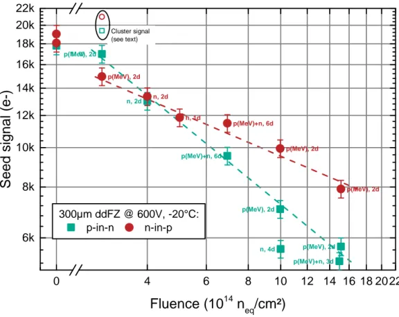
for sensors with a nominal active thickness of 300 µm. The faster decrease of the collected charge with fluence can be clearly seen for p-in-n type sensors compared to n-in-p type sensors, which is in
line with results from RD50,3e.g. [40]. With increasing fluence, trapping effects [41,42] become
more and more dominant and hole collection (at p-type strips) is a clear disadvantage due to the
much lower mobility and therefore longer drift time of the holes. In figure8a lower seed signal
is observed for n-in-p type sensors at the first irradiation step of 3 × 10¹⁴neq/cm2, which is due to
wider clusters in those sensors resulting in a smaller seed signal. This difference can originate from
2017 JINST 12 P06018
0 5 1 0 1 5 1 M 1 0 M 1 0 0 M 1 G 1 0 G 1 0 0 G 1 T 1 0 T 1 0 0 T1 0 0 M
Ω
c m
In
te
rs
tr
ip
r
e
s
is
ta
n
c
e
(
Ω
c
m
)
F l u e n c e ( 1 0
1 4n
e q/ c m ² )
F Z 2 0 0 µ m n - i n - p t y p e p - s t o p p - s p r a y F Z 2 0 0 µ m p - i n - n t y p e D a t a s e t : > 1 0 m e a s u r e m e n t s f o r 6 0 0 V < U b i a s< 8 0 0 V ( i r r a d . ) , 3 0 0 V < U b i a s< 5 0 0 V ( n o n - i r r a d . ) S y m b o l s : m e a n v a l u e s B a n d s s p a n b e t w e e n m i n . a n d m a x . v a l u e sFigure 7. Interstrip resistance to the neighboring strip vs. irradiation fluence for nominal 200 µm thick
sensors. The resistance is normalized to 1 cm strip length. Each data point indicates the mean of at least ten measurements (different strips on same sensor) on fully depleted sensors. The bands indicate the maximum and minimum values measured. Measurements on non-irradiated samples were performed at
room temperature, else at −20◦C.
the positive oxide charge generated by ionizing radiation [8,10] leading to an electron accumulation
in the n-in-p type sensors and a resulting alteration of the electric fields close to the strips [43]. The
total cluster signal is similar to (or in this example even exceeds) the one from p-in-n type sensors
at this fluence as indicated by the open symbols in figure8.
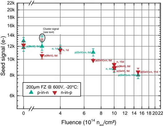
Looking at the charge collection of sensors with a nominal active thickness of 200 µm (figure9)
the difference of collecting electrons versus holes is not visible due to the higher electric field at the same bias voltage of 600 V. The plot also shows the seed signals of three different particle
types at the fluence point 1 × 10¹⁵neq/cm2, which are very closely spread around 9000 e− and
demonstrate that the particle type does not change the results significantly. Also in figure9one can
see the difference of measured cluster charge (open symbols) versus seed charge after an irradiation
fluence of 3 × 10¹⁴neq/cm2 for 200 µm. One could conclude from the seed signals in figure 9
that p-in-n sensors are compatible or slightly superior to n-in-p. This assessment changes when looking at the noise performance. For irradiated p-in-n sensors with a nominal active thickness of 200 µm a strong non-Gaussian noise component on all strips was observed, which cannot be
2017 JINST 12 P06018
0 4 6 8 1 0 1 2 1 4 1 6 1 8 2 0 2 2 6 k 8 k 1 0 k 1 2 k 1 4 k 1 6 k 1 8 k 2 0 k 2 2 k p ( M e V ) , 2 d n , 2 d p ( M e V ) + n , 6 d p ( M e V ) , 2 d n , 4 d p ( M e V ) + n , 3 d p ( M e V ) , 2 d p ( M e V ) , 2 d n , 2 d n , 1 d p ( M e V ) + n , 6 d p ( M e V ) , 2 d p ( M e V ) , 2 d 3 0 0 µ m d d F Z @ 6 0 0 V , - 2 0 ° C : p - i n - n n - i n - pS
e
e
d
s
ig
n
a
l
(e
-)
F l u e n c e ( 1 0
1 4n
e q/ c m ² )
C l u s t e r s i g n a l ( s e e t e x t ) M e VFigure 8. Charge collected on the seed strip for sensors of a nominal active thickness of 300 µm after a
short annealing time of between 2 and 6 days at room temperature. The error bars reflect an estimated uncertainty of about 5% representing statistical and gain uncertainties. The text next to the symbols indicates the irradiation type (p stands for protons with energy range MeV/GeV and n for neutrons) and the equivalent
annealing time at 21◦C. The lines should guide the eye.
of noise distributions with and without the non-Gaussian component are shown in figure10, for
which the average over all events per channel (pedestal) was subtracted from the raw data. It is obvious that applying a threshold of 5σ of the Gaussian fit does not eliminate misidentified hits due to the long noise tails. To quantify this effect a 5σ threshold was applied to these distributions and the misidentification occupancy was calculated by summing up all entries above this threshold
and dividing by the number of events and the number of active read-out strips. Figure 11shows
several plots of this quantity as a function of bias voltage and equivalent annealing time at room
temperature.4 A significantly large area (red) represents operation conditions under which the
sensors show a misidentified hit occupancy above 1%. This value is considered severe since one expects an occupancy of real particle hits of the same amount in the future outer tracker. These
misidentified hits are already observed at a proton fluence of 3 × 10¹⁴neq/cm2. The occupancy
4Annealing is performed at elevated temperatures and the acceleration factor of the current annealing from [27] was applied.
2017 JINST 12 P06018
0 4 6 8 1 0 1 2 1 4 1 6 1 8 2 0 2 2 6 k 8 k 1 0 k 1 2 k 1 4 k 1 6 k 1 8 k 2 0 k 2 2 k p ( G e V ) + n , 6 d p ( M e V ) , 0 d n , 1 d n , 4 d p ( G e V ) + n , 1 5 d p ( G e V ) + n , 6 d p ( G e V ) , 9 d p ( G e V ) + n , 1 1 d p ( M e V ) , 0 d n , 1 d p ( M e V ) , 0 d n , 1 5 d C l u s t e r s i g n a l ( s e e t e x t ) 2 0 0 µ m F Z @ 6 0 0 V , - 2 0 ° C : p - i n - n n - i n - pS
e
e
d
s
ig
n
a
l
(e
-)
F l u e n c e ( 1 0
1 4n
e q/ c m ² )
M e VFigure 9. Charge collected on the seed strip for sensors with a nominal active thickness of 200 µm after
a short annealing time of between 0 and 15 days at room temperature. The error bars reflect an estimated uncertainty of about 5% representing statistical and gain uncertainties. The text next to the symbols indicates the irradiation type (p stands for protons with energy range MeV/GeV and n for neutrons) and the equivalent
annealing time at 21◦C.
Pedestal subtracted noise (ADC counts) 200 − −150 −100 −50 0 50 100 150 200 Counts 1 10 2 10 3 10 4 10
Pedestal subtracted noise (ADC counts) 200 − −150 −100 −50 0 50 100 150 200 Counts 10 2 10 3 10 4 10
Figure 10. Two examples of pedestal-subtracted noise distributions as measured with the ALiBaVa system
and fitted by a Gaussian distribution: a normal noise distribution (left) as observed on p-in-n type FZ sensors before irradiation, which looks similar for n-in-p sensors (both non-irradiated and irradiated), and a noise distribution affected by the non-Gaussian component observed for irradiated p-in-n FZ sensors with a nominal active thickness of 200 µm (right).
2017 JINST 12 P06018
1 0 1 0 0 1 0 0 0 1 0 0 0 0 2 0 0 4 0 0 6 0 0 8 0 0 1 0 0 0 2 0 0 µ m p - i n - n F = 3 x 1 0 1 4 n e q/ c m 2 ( p G e V) + 4 x 1 01 4 n e q/ c m 2 ( n ) B ia s v o lt a g e ( V ) E q . a n n e a l i n g t i m e a t + 2 1 ° C ( h ) 0 . 0 5 % 0 . 0 7 % 0 . 1 1 % 0 . 1 5 % 0 . 2 2 % 0 . 3 3 % 0 . 4 7 % 0 . 6 9 % 1 . 0 0 % 1 0 1 0 0 1 0 0 0 1 0 0 0 0 2 0 0 4 0 0 6 0 0 8 0 0 1 0 0 0 F = 1 x 1 0 2 0 0 µ m p - i n - n 1 5 n e q/ c m 2 ( p G e V) + 5 x 1 0 1 4 n e q/ c m 2 ( n ) B ia s v o lt a g e ( V ) E q . a n n e a l i n g t i m e a t + 2 1 ° C ( h ) 0 . 0 5 % 0 . 0 7 % 0 . 1 1 % 0 . 1 5 % 0 . 2 2 % 0 . 3 3 % 0 . 4 7 % 0 . 6 9 % 1 . 0 0 % 1 0 1 0 0 1 0 0 0 1 0 0 0 0 2 0 0 4 0 0 6 0 0 8 0 0 1 0 0 0 F = 1 x 1 0 1 5n e q/ c m 2 ( n ) 2 0 0 µ m p - i n - n B ia s v o lt a g e ( V ) E q . a n n e a l i n g t i m e a t + 2 1 ° C ( h ) 0 . 0 5 % 0 . 0 7 % 0 . 1 1 % 0 . 1 5 % 0 . 2 2 % 0 . 3 3 % 0 . 4 7 % 0 . 6 9 % 1 . 0 0 %Figure 11. Measured occupancy of misidentified hits generated by non-Gaussian noise. These examples
are for p-in-n sensors with 200 µm active and physical thickness irradiated to 7 × 10¹⁴n
eq/cm2 (top) and
1.5 × 10¹⁵n
eq/cm2(center) with mixed particles and to 1 × 10¹⁵neq/cm2with only neutrons (bottom). The
black dots represent the data points and the color code interpolates between them. White areas lie outside the measurement range.
2017 JINST 12 P06018
1 0 1 0 0 1 0 0 0 1 0 0 0 0 2 0 0 4 0 0 6 0 0 8 0 0 1 0 0 0 F = 1 x 1 01 5 ne q/ c m 2 ( p G e V) + 5 x 1 01 4 n e q/ c m 2 ( n ) 2 0 0 µ m n - i n - p B ia s v o lt a g e ( V ) E q . a n n e a l i n g t i m e a t + 2 1 ° C ( h ) 0 . 0 5 % 0 . 0 7 % 0 . 1 1 % 0 . 1 5 % 0 . 2 2 % 0 . 3 3 % 0 . 4 7 % 0 . 6 9 % 1 . 0 0 %Figure 12. Measured occupancy of misidentified hits generated by non-Gaussian noise. This example is for
an n-in-p type sensor with a nominal active and physical thickness of 200 µm irradiated to 1.5 × 10¹⁵neq/cm2
mixed fluence.
increases with temperature and it strongly depends on the applied bias voltage, which suggests that the non-Gaussian noise originates from high electric fields. This coincides with the finding that thin sensors with a higher maximum electric field at the same bias voltage are more affected. In addition, it was observed that p-in-n sensors irradiated only with neutrons also show misidentified
hits but at higher bias voltages (figure11(bottom)).
Non-Gaussian noise was not observed in n-in-p type sensors as can be seen from figure12. To
reproduce and understand this effect, TCAD simulations were performed. These simulations are discussed in the next section.
5 Simulation of electric fields
For the device simulations, the commercial TCAD software packages from Synopsys [46] and
Silvaco [47] were used. Effective defect models were developed in [38,48] for proton and neutron
irradiated sensors. The defect properties of the model in Synopsys tuned to data from proton
irradiated samples are listed in table 3. The electric field in the region between two strips of
a 200 µm thick strip sensor was simulated at a bias voltage of 1000 V (higher bias voltage than nominal operation voltage of 600 V to enhance high field effects; qualitative differences are not
expected) with bulk defect concentrations corresponding to a fluence of 1 × 10¹⁵neq/cm2 for a
p-in-n and an n-in-p configuration. The surface damage was introduced by increasing the fixed
oxide charge at the Si-SiO2 interface. The electric field strength at 1.3 µm below the Si-SiO2
interface (approximate depth of the strip doping profile) is plotted in figure13for the two different
configurations. The two plots show that the maximum electric field is always at the strip edge for both configurations and that for p-in-n type sensors the electric field increases with increasing
oxide charge (Nox), while it decreases for n-in-p type sensors. Such an increase in oxide charge
(fast increase and saturation around 2 × 1012cm−2at 10 kGy [7,8]) is expected due to the ionizing
2017 JINST 12 P06018
0 1 0 2 0 3 0 4 0 5 0 6 0 7 0 8 0 9 0 0 . 0 5 0 . 0 k 1 0 0 . 0 k 1 5 0 . 0 k 2 0 0 . 0 k 2 5 0 . 0 k 3 0 0 . 0 k F = 1 x 1 01 5n e q/ c m 2; T = - 2 0 ° C ; V b i a s= 1 0 0 0 V E le c tr ic f ie ld / ( V /c m ) I n t e r - s t r i p p o s i t i o n / (µm ) N O x= 1 x 1 01 1 c m - 2 N O x= 1 x 1 01 2 c m - 2 p - i n - n p + A l u - s t r i p p + A l u - s t r i p 0 1 0 2 0 3 0 4 0 5 0 6 0 7 0 8 0 9 0 0 . 0 5 0 . 0 k 1 0 0 . 0 k 1 5 0 . 0 k 2 0 0 . 0 k 2 5 0 . 0 k 3 0 0 . 0 k p - s t o p E le c tr ic f ie ld / ( V /c m ) I n t e r - s t r i p p o s i t i o n / (µm ) N O x= 1 x 1 0 1 1 c m - 2 N O x= 1 x 1 0 1 2 c m - 2 n + A l u - s t r i p F = 1 x 1 01 5 ne q/ c m 2 ; T = - 2 0 ° C ; Vb i a s= - 1 0 0 0 V n - i n - p n + A l u - s t r i pFigure 13. Simulated electric field strength 1.3 µm below the Si-SiO2 interface after bulk damage
equiv-alent to 1 × 10¹⁵neq/cm2 at 1000 V bias voltage and a temperature of −20◦C. N
ox of 1 × 1011cm−2 and
1 × 1012cm−2 correspond approximately to a total ionizing dose of 10 Gy and 10 kGy, respectively. The
upper part of the plot includes a sketch of the surface layout. The upper plot represents a p-in-n type sensor
and the lower plot an n-in-p type sensor [49]. The simulations were performed with Synopsys TCAD.
Table 3. Properties of the two bulk defects used for the simulations. EV and EC are the energies of the
valence and conduction band, respectively, while σ(e) and σ(h) are the cross sections for electrons and holes
and F stands for the fluence [48].
Parameter Defect 1 Defect 2
Type Donor Acceptor
Energy (eV) EV+0.48 EC-0.525
Concentration (cm−3) 5.598 cm−1×F - 3.949 · 1014 1.189 cm−1×F - 6.454 · 1013
σ(e) (cm2) 1.0 · 10−14 1.0 · 10−14
2017 JINST 12 P06018
the validation at the expected radiation conditions. Similar simulations were carried out usingSilvaco and a slightly modified defect model resulting in the same conclusion being drawn [38,45].
The outcome of the simulations could explain the tails observed in the pedestal-subtracted noise
distributions of figure 10 for p-in-n type sensors: thermally generated charge carriers could be
accelerated in the high electric field regions found in the simulations and be subject to an avalanche type multiplication generating a random signal.
The simulation results confirm that after radiation exposure to the expected doses for HL-LHC, sensors with the n-in-p type configuration are a more robust choice for the CMS Tracker application. Since this qualitative result is obtained with a 2D simulation taking into account only a slice of 1 µm it is valid for long strips as well as shorter macro-pixel sensors. The small potential difference on the implanted strips of AC and DC coupled sensors is not expected to change the conclusion.
While an adaptation of the design could lead to robust p-in-n sensors, as shown in [50,51], this was
not investigated by the collaboration.
6 Conclusion
A variety of different silicon base materials and technologies were investigated using sensors and test structures produced by a single manufacturer. Miniature strip sensors were characterized before and after irradiations up to the levels expected for the HL-LHC operation period. The characterizations included electrical measurements of the sensor parameters, charge collection, noise occupancy measurements and annealing studies.
Comparing the performance of the sensors the collaboration has concluded that n-in-p type sensors are the most appropriate choice for operation in the CMS outer tracker region at HL-LHC. The main considerations were:
• It was confirmed that strip isolation of n-in-p sensors can be well controlled using either p-stop or p-spray technology.
• Sensors with n-type readout strips mainly collecting electrons provide equivalent or higher
signals after irradiations beyond 5 × 10¹⁴neq/cm2than achieved for p-in-n sensors for equal
thickness and bias voltage.
• The investigated p-in-n type sensors show non-Gaussian noise effects after irradiation related to high electric fields, while n-in-p type sensors do not.
• Compared to n-in-n type sensors, the n-in-p process is single-sided and presumably available at lower costs. Also the n-in-p sensors are less sensitive to scratches on the back side. Acknowledgments
The research leading to these results has received funding from the European Commission under the FP7 Research Infrastructures project AIDA, Grant agreement no. 262025.
2017 JINST 12 P06018
References[1] http://hilumilhc.web.cern.ch/about/hl-lhc-project.
[2] I. Bejar Alonso, L. Rossi, HiLumi LHC Technical Design Report,CERN-ACC-2015-0140(2015).
[3] D. Contardo et al., Technical Proposal for the Phase-II Upgrade of the CMS Detector,
CERN-LHCC-2015-010.
[4] CMS collaboration, The CMS Experiment at the CERN LHC,2008 JINST 3 S08004.
[5] CMS collaboration, 1-D plot covering CMS tracker, showing FLUKA simulated 1 MeV neutron
equivalent in Silicon including contributions from various particle types.,CMS-DP-2015-022.
[6] M. Huhtinen, Simulation of non-ionising energy loss and defect formation in silicon,Nucl. Instrum.
Meth. A 491(2002) 194.
[7] J. Zhang, X-ray Radiation Damage Studies and Design of a Silicon Pixel Sensor for Science at the
XFEL, DESY (2013) [DESY-THESIS-13-018].
[8] J. Zhang et al., Study of radiation damage induced by 12 keV X-rays in MOS structures built on
high-resistivity n-type silicon, J. Synchrotron Rad. 19 (2012) 340.
[9] T.P. Ma and P. Dressendorfer, Ionizing Radiation Effects in MOS Devices and Circuits, Wiley (1989) [ISBN: 978-0-471-84893-6].
[10] T.R. Oldham and F.B. McLean, Total ionizing dose effects in MOS oxides and devices,IEEE Trans.
Nucl. Sci. 50(2003) 483.
[11] K.H. Hoffmann, Campaign to identify the future CMS tracker baseline,Nucl. Instrum. Meth. A 658
(2011) 30.
[12] G. Auzinger, Silicon sensor development for the CMS tracker upgrade,2011 JINST 6 P10010.
[13] G. Steinbrück on behalf of the CMS Tracker collaboration, Towards radiation hard sensor materials
for the CMS tracker upgrade, in proceedings ofIEEE Nuclear Science Symposium and Medical Imaging Conference (NSS/MIC), 2012, pp. 1828–1832.
[14] A. Dierlamm, Characterisation of silicon sensor materials and designs for the CMS Tracker Upgrade,
PoS(VERTEX 2012)016.
[15] D. Eckstein, CMS outer tracker upgrade plans,PoS(VERTEX2013)015.
[16] B. Lutzer, Characterization of irradiated test structures for the CMS tracker upgrade,Nucl. Instrum.
Meth. A 730(2013) 204.
[17] G. Auzinger, Analysis of testbeam data of irradiated silicon prototype sensors for the CMS tracker
upgrade,Nucl. Instrum. Meth. A 730(2013) 195.
[18] A. Junkes, Planar silicon sensors for the CMS tracker upgrade,Nucl. Instrum. Meth. A 732(2013)
113.
[19] A. Nürnberg and T. Schneider, Lorentz angle measurements as part of the sensor R&D for the CMS
Tracker upgrade,2013 JINST 8 C01001.
[20] M. Bernard-Schwarz, Future silicon sensors for the CMS Tracker upgrade,Nucl. Instrum. Meth. A
699(2013) 89.
[21] CMS Tracker collaboration, M. Printz, Radiation hard sensor materials for the CMS Tracker Phase
2017 JINST 12 P06018
[22] G. Lutz, Semiconductor Radiation Detectors — Device Physics, Springer (1999) [ISBN 3-540-64859-3].
[23] A. Junkes, Influence of radiation induced defect clusters on silicon particle detectors, Ph.D. thesis, University of Hamburg (2011) [DESY-THESIS-2011-031].
[24] CMS collaboration, The CMS tracker system project: Technical Design Report,CERN-LHCC-98-006
(1997).
[25] CMS collaboration, The CMS tracker: addendum to the Technical Design Report,
CERN-LHCC-2000-016(2000).
[26] M. Huhtinen, The radiation environment at the CMS experiment at the LHC, Ph.D. thesis, Helsinki U.
Tech. (1996) [HU-SEFT-R-1996-14].
[27] M. Moll, Radiation Damage in Silicon Particle Detectors, Ph.D. thesis, University of Hamburg (1999), [DESY-THESIS-1999-040].
[28] L. Snoj, G. Žerovnik and A. Trkov, Computational analysis of irradiation facilities at the JSI TRIGA
reactor,Appl. Radiat. Isotopes 70(2012) 483.
[29] D. Zontar, V. Cindro, G. Kramberger and M. Mikuz, Time development and flux dependence of
neutron-irradiation induced defects in silicon pad detectors,Nucl. Instrum. Meth. A 426(1999) 51.
[30] https://ps-irrad.web.cern.ch/.
[31] http://www.ekp.kit.edu/english/irradiation_center.php.
[32] K.-H. Hoffmann, Development of new Sensor Designs and Investigations on Radiation Hard Silicon
Strip Sensors for the CMS Tracker Upgrade at the High Luminosity Large Hadron Collider, Ph.D.
thesis, Karlsruhe Institute of Technology (2013) [IEKP-KA/2013-1].
[33] R. Marco-Hernandez, A portable readout system for silicon microstrip sensors,Nucl. Instrum. Meth.
A 623(2010) 207,http://www.alibavasystems.com.
[34] The Beetle Reference Manual for Beetle version 1.3 / 1.4 / 1.5, LHCb-2005-105,
http://www.kip.uni-heidelberg.de/lhcb/Publications/BeetleRefMan_v1_3.pdf.
[35] S. Löchner, Development, Optimisation and Characterisation of a Radiation Hard Mixed-Signal
Readout Chip for LHCb, Ph.D. thesis, Combined Faculties for the Natural Sciences and for
Mathematics of the Ruperto-Carola University of Heidelberg, Germany (2006) [http://archiv.ub.uni-heidelberg.de/volltextserver/6708/].
[36] G. Hall et al., CBC2: A CMS microstrip readout ASIC with logic for track-trigger modules at
HL-LHC,Nucl. Instrum. Meth. A 765(2014) 214.
[37] H. Bichsel, Straggling in Thin Silicon Detectors,Rev. Mod. Phys. 60(1988) 663.
[38] R. Dalal, A. Bhardwaj, K. Ranjan, M. Moll and A. Elliott-Peisert, Combined effect of bulk and
surface damage on strip insulation properties of proton irradiated n+-p silicon strip sensors,2014
JINST 9P04007.
[39] M. Printz, P-stop isolation study of irradiated n-in-p type silicon strip sensors for harsh radiation
environments,Nucl. Instrum. Meth. A 831(2016) 38.
[40] A. Affolder, P. Allport and G. Casse, Collected charge of planar silicon detectors after pion and
proton irradiations up to2.2 × 1016neqcm−2,Nucl. Instrum. Meth. A 623(2010) 177.
[41] CMS Tracker Group collaboration, Trapping in proton irradiated p+-n-n+silicon sensors at
2017 JINST 12 P06018
[42] G. Kramberger, V. Cindro, I. Mandic, M. Mikuz and M. Zavrtanik, Effective trapping time of
electrons and holes in different silicon materials irradiated with neutrons, protons and pions,Nucl. Instrum. Meth. A 481(2002) 297.
[43] CMS Tracker Group collaboration, Impact of low-dose electron irradiation on n+p silicon strip
sensors,Nucl. Instrum. Meth. A 803(2015) 100[arXiv:1505.02672].
[44] A. Dierlamm, Planar sensors for future Vertex and Tracking Detectors,PoS(VERTEX2013)027.
[45] R. Dalal, Simulation of Irradiated Detectors,PoS(VERTEX2014)030.
[46] https://www.synopsys.com/silicon/tcad.html. [47] Silvaco Inc., Atlas Users Manual,
https://dynamic.silvaco.com/dynamicweb/jsp/downloads/DownloadManualsAction.do?req=silen-manuals&nm=atlas.
[48] R. Eber, Investigations of new Sensor Designs and Development of an effective Radiation Damage
Model for the Simulation of highly irradiated Silicon Particle Detectors, Ph.D. thesis, Karlsruhe
Institute of Technology (2013), [IEKP-KA/2013-27].
[49] M. Printz, T-CAD analysis of electric fields in n-in-p silicon strip detectors in dependence on the
p-stop pattern and doping concentration,2015 JINST 10 C01048.
[50] J. Schwandt, E. Fretwurst, R. Klanner, I. Kopsalis and J. Zhang, Design and First Tests of a
Radiation-Hard Pixel Sensor for the European X-Ray Free-Electron Laser,IEEE Trans. Nucl. Sci. 61
(2014) 1894[arXiv:1402.3129].
[51] J. Schwandt, Design of a Radiation Hard Silicon Pixel Sensor for X-ray Science, Ph.D. thesis, University of Hamburg (2014) [DESY-THESIS-2014-029].
2017 JINST 12 P06018
Tracker group of the CMS collaborationInstitut für Hochenergiephysik, Wien, Austria
W. Adam, T. Bergauer, E. Brondolin, M. Dragicevic, M. Friedl, R. Frühwirth,1M. Hoch,
J. Hrubec, A. König, H. Steininger, W. Waltenberger
Universiteit Antwerpen, Antwerpen, Belgium
S. Alderweireldt, W. Beaumont, X. Janssen, J. Lauwers, P. Van Mechelen, N. Van Remortel, A. Van Spilbeeck
Université Libre de Bruxelles, Bruxelles, Belgium
D. Beghin, H. Brun, B. Clerbaux, H. Delannoy, G. De Lentdecker, G. Fasanella, L. Favart, R. Goldouzian, A. Grebenyuk, G. Karapostoli, Th. Lenzi, A. Léonard, J. Luetic, N. Postiau, T. Seva, P. Vanlaer, D. Vannerom, Q. Wang, F. Zhang
Vrije Universiteit Brussel, Brussel, Belgium
S. Abu Zeid, F. Blekman, I. De Bruyn, J. De Clercq, J. D’Hondt, K. Deroover, S. Lowette, S. Moortgat, L. Moreels, Q. Python, K. Skovpen, P. Van Mulders, I. Van Parijs
Université Catholique de Louvain, Louvain-la-Neuve, Belgium
H. Bakhshiansohi, O. Bondu, S. Brochet, G. Bruno, A. Caudron, C. Delaere, M. Delcourt, S. De Visscher, B. Francois, A. Giammanco, A. Jafari, M. Komm, G. Krintiras, V. Lemaitre, A. Magitteri, A. Mertens, D. Michotte, M. Musich, K. Piotrzkowski, L. Quertenmont, N. Szilasi, M. Vidal Marono, S. Wertz
Université de Mons, Mons, Belgium
N. Beliy, T. Caebergs, E. Daubie, G.H. Hammad
Helsinki Institute of Physics, Helsinki, Finland
J. Härkönen, T. Lampén, P. Luukka, T. Peltola, E. Tuominen, E. Tuovinen
Department of Physics, University of Helsinki, Helsinki, Finland
P. Eerola
Lappeenranta University of Technology, Lappeenranta, Finland
T. Tuuva
Université de Lyon, Université Claude Bernard Lyon 1, CNRS-IN2P3, Institut de Physique Nucléaire de Lyon, Villeurbanne, France
G. Baulieu, G. Boudoul, L. Caponetto, C. Combaret, D. Contardo, T. Dupasquier, G. Gallbit, N. Lumb, L. Mirabito, S. Perries, M. Vander Donckt, S. Viret
Université de Strasbourg, CNRS, IPHC UMR 7178, Strasbourg, France
J.-L. Agram,2J. Andrea, D. Bloch, C. Bonnin, J.-M. Brom, E. Chabert, N. Chanon, L. Charles,
E. Conte,2J.-Ch. Fontaine,2L. Gross, J. Hosselet, M. Jansova, D. Tromson
RWTH Aachen University, I. Physikalisches Institut, Aachen, Germany
C. Autermann, L. Feld, W. Karpinski, K.M. Kiesel, K. Klein, M. Lipinski, A. Ostapchuk, G. Pierschel, M. Preuten, M. Rauch, S. Schael, C. Schomakers, J. Schulz, G. Schwering, M. Wlochal, V. Zhukov
2017 JINST 12 P06018
RWTH Aachen University, III. Physikalisches Institut B, Aachen, Germany
C. Pistone, G. Fluegge, A. Kuensken, O. Pooth, A. Stahl
Deutsches Elektronen-Synchrotron, Hamburg, Germany
M. Aldaya, C. Asawatangtrakuldee, K. Beernaert, D. Bertsche, C. Contreras-Campana,
G. Eckerlin, D. Eckstein, T. Eichhorn, E. Gallo, J. Garay Garcia, K. Hansen, M. Haranko, A. Harb,
J. Hauk, J. Keaveney, A. Kalogeropoulos, C. Kleinwort, W. Lohmann,3R. Mankel, H. Maser,
G. Mittag, C. Muhl, A. Mussgiller, D. Pitzl, O. Reichelt, M. Savitskyi, P. Schuetze, R. Walsh, A. Zuber
University of Hamburg, Hamburg, Germany
H. Biskop, P. Buhmann, M. Centis-Vignali, E. Garutti, J. Haller, M. Hoffmann, T. Lapsien, M. Matysek, A. Perieanu, Ch. Scharf, P. Schleper, A. Schmidt, J. Schwandt, J. Sonneveld, G. Steinbrück, B. Vormwald, J. Wellhausen
Institut für Experimentelle Kernphysik, Karlsruhe, Germany
M. Abbas, C. Amstutz, T. Barvich, Ch. Barth, F. Boegelspacher, W. De Boer, E. Butz, M. Caselle, F. Colombo, A. Dierlamm, B. Freund, F. Hartmann, S. Heindl, U. Husemann, A. Kornmayer, S. Kudella, Th. Muller, H.J. Simonis, P. Steck, M. Weber, Th. Weiler
Institute of Nuclear and Particle Physics (INPP), NCSR Demokritos, Aghia Paraskevi, Greece
G. Anagnostou, P. Asenov, P. Assiouras, G. Daskalakis, A. Kyriakis , D. Loukas, L. Paspalaki
Wigner Research Centre for Physics, Budapest, Hungary
F. Siklér, V. Veszprémi
University of Delhi, Delhi, India
A. Bhardwaj, R. Dalal, G. Jain, K. Ranjan
Institute for Research in Fundamental Sciences (IPM), Tehran, Iran
H. Bakhshiansohl, H. Behnamian, M. Khakzad, M. Naseri
INFN Sezione di Bari,aUniversità di Bari,bPolitecnico di Bari,cBari, Italy
P. Cariola,aD. Creanza,a,cM. De Palma,a,b G. De Robertis,aL. Fiore,aM. Franco,aF. Loddo,a
L. Silvestris,aG. Maggi,a,cS. Martiradonna,aS. My,a,bG. Selvaggia,b
INFN Sezione di Catania,aUniversità di Catania,b Catania, Italy
S. Albergo,a,b G. Cappello,a,bM. Chiorboli,a,b S. Costa,a,b A. Di Mattia,aF. Giordano,a,b
R. Potenza,a,b M.A. Saizu,a,4A. Tricomi,a,b C. Tuvea,b
INFN Sezione di Firenze,aUniversità di Firenze,bFirenze, Italy
G. Barbagli,aM. Brianzi,aR. Ciaranfi,aV. Ciulli,a,b C. Civinini,aR. D’Alessandro,a,b
E. Focardi,a,b G. Latino,a,b P. Lenzi,a,b M. Meschini,aS. Paoletti,aL. Russo,a,b E. Scarlini,a,b
G. Sguazzoni,aD. Strom,aL. Viliania,b
INFN Sezione di Genova,aUniversità di Genova,b Genova, Italy
2017 JINST 12 P06018
INFN Sezione di Milano-Bicocca,aUniversità di Milano-Bicocca,b Milano, Italy
M.E. Dinardo,a,b S. Fiorendi,a,bS. Gennai,aS. Malvezzi,aR.A. Manzoni,a,b D. Menasce,a
L. Moroni,aD. Pedrinia
INFN Sezione di Padova,aUniversità di Padova,bPadova, Italy
P. Azzi,aN. Bacchetta,aD. Bisello,aM. Dall’Osso,a,b N. Pozzobon,a,b M. Tosia,b
INFN Sezione di Pavia,aUniversità di Bergamo,bItaly
F. De Canio,a,b L. Gaioni,a,b M. Manghisoni,a,b B. Nodari,a,b E. Riceputi,a,b V. Re,a,b
G. Traversia,b
INFN Sezione di Pavia,aUniversità di Pavia,b Pavia, Italy
D. Comotti,a,b L. Rattia,b
INFN Sezione di Perugia,aUniversità di Perugia,bPerugia, Italy
L. Alunni Solestizi,a,b M. Biasini,a,bG.M. Bilei,aC. Cecchi,a,b B. Checcucci,a
D. Ciangottini,a,b L. Fanò,a,bC. Gentsos,aM. Ionica,aR. Leonardi,a,bE. Manoni,a,b
G. Mantovani,a,b S. Marconi,a,b V. Mariani,a,b M. Menichelli,aA. Modak,a,b A. Morozzi,a,b
F. Moscatelli,aD. Passeri,a,b P. Placidi,a,b V. Postolache,aA. Rossi,a,b A. Saha,a
A. Santocchiaa,b L. Storchi,aD. Spigaa
INFN Sezione di Pisa,aUniversità di Pisa,b Scuola Normale Superiore di Pisa,cPisa, Italy
K. Androsov,a,5P. Azzurri,aS. Arezzini,aG. Bagliesi,aA. Basti,aT. Boccali,aL. Borrello,a
F. Bosi,aR. Castaldi,aA. Ciampa,aM.A. Ciocci,a,6R. Dell’Orso,aS. Donato,a,cG. Fedi,a
A. Giassi,aM.T. Grippo,a,6F. Ligabue,a,cT. Lomtadze,aG. Magazzu,aL. Martini,a,b
E. Mazzoni,aA. Messineo,a,b A. Moggi,aF. Morsani,aF. Palla,aF. Palmonari,aF. Raffaelli,a
A. Rizzi,a,b A. Savoy-Navarro,a,7P. Spagnolo,aR. Tenchini,aG. Tonelli,a,bA. Venturi,a
P.G. Verdinia
INFN Sezione di Torino,aUniversità di Torino,bTorino, Italy
R. Bellan,a,b M. Costa,a,b R. Covarelli,a,bM. Da Rocha Rolo,aN. Demaria,aA. Rivetti,a
G. Dellacasa,aG. Mazza,aE. Migliore,a,b E. Monteil,a,b L. Pacher,aF. Ravera,a,b A. Solanoa,b
Instituto de Física de Cantabria (IFCA), CSIC-Universidad de Cantabria, Santander, Spain
M. Fernandez, G. Gomez, R. Jaramillo Echeverria, D. Moya, F.J. Gonzalez Sanchez, I. Vila, A.L. Virto
CERN, European Organization for Nuclear Research, Geneva, Switzerland
D. Abbaneo, I. Ahmed, E. Albert, G. Auzinger, G. Berruti, G. Bianchi, G. Blanchot, J. Bonnaud, A. Caratelli, D. Ceresa, J. Christiansen, K. Cichy, J. Daguin, A. D’Auria, S. Detraz, D. Deyrail, O. Dondelewski, F. Faccio, N. Frank, T. Gadek, K. Gill, A. Honma, G. Hugo, L.M. Jara Casas,
J. Kaplon, A. Kornmayer, L. Kottelat, M. Kovacs, M. Krammer,1P. Lenoir, M. Mannelli,
A. Marchioro, S. Marconi, S. Mersi, S. Martina, S. Michelis, M. Moll, A. Onnela, S. Orfanelli, S. Pavis, A. Peisert, J.-F. Pernot, P. Petagna, G. Petrucciani, H. Postema, P. Rose, P. Tropea, J. Troska, A. Tsirou, F. Vasey, P. Vichoudis, B. Verlaat, L. Zwalinski
2017 JINST 12 P06018
Institute for Particle Physics, ETH Zurich, Zurich, Switzerland
F. Bachmair, R. Becker, D. di Calafiori, B. Casal, P. Berger, L. Djambazov, M. Donega, C. Grab, D. Hits, J. Hoss, G. Kasieczka, W. Lustermann, B. Mangano, M. Marionneau,
P. Martinez Ruiz del Arbol, M. Masciovecchio, M. Meinhard, L. Perozzi, U. Roeser,
A. Starodumov,8V. Tavolaro, R. Wallny, D. Zhu
Universität Zürich, Zurich, Switzerland
C. Amsler,9K. Bösiger, L. Caminada, F. Canelli, V. Chiochia, A. de Cosa, C. Galloni, T. Hreus,
B. Kilminster, C. Lange, R. Maier, J. Ngadiuba, D. Pinna, P. Robmann, S. Taroni, Y. Yang
Paul Scherrer Institut, Villigen, Switzerland
W. Bertl†, K. Deiters, W. Erdmann, R. Horisberger, H.-C. Kaestli, D. Kotlinski, U. Langenegger,
B. Meier, T. Rohe, S. Streuli
National Taiwan University (NTU), Taipei, Taiwan
P.-H. Chen, C. Dietz, U. Grundler, W.-S. Hou, R.-S. Lu, M. Moya
University of Bristol, Bristol, United Kingdom
D. Cussans, H. Flacher, J. Goldstein, M. Grimes, J. Jacob, S. Seif El Nasr-Storey
Brunel University, Uxbridge, United Kingdom
J. Cole, C. Hoad, P. Hobson, A. Morton, I.D. Reid
Imperial College, London, United Kingdom
G. Auzinger, R. Bainbridge, P. Dauncey, G. Hall, T. James, A.-M. Magnan, M. Pesaresi, D.M. Raymond, K. Uchida
Rutherford Appleton Laboratory, Didcot, United Kingdom
J.A. Coughlan, K. Harder, J. Ilic, I.R. Tomalin
Brown University, Providence, U.S.A.
A. Garabedian, U. Heintz, M. Narain, J. Nelson, S. Sagir, T. Speer, J. Swanson, D. Tersegno, J. Watson-Daniels
University of California, Davis, Davis, U.S.A.
M. Chertok, J. Conway, R. Conway, C. Flores, R. Lander, D. Pellett, F. Ricci-Tam, M. Squires, J. Thomson, R. Yohay
University of California, Riverside, Riverside, U.S.A.
K. Burt, J. Ellison, G. Hanson, M. Olmedo, W. Si, B.R. Yates
University of California, San Diego, La Jolla, U.S.A.
R. Gerosa, V. Sharma, A. Vartak, A. Yagil, G. Zevi Della Porta
University of California, Santa Barbara — Department of Physics, Santa Barbara, U.S.A.
V. Dutta, L. Gouskos, J. Incandela, S. Kyre, S. Mullin, A. Patterson, H. Qu, D. White
The Catholic University of America, Washington DC, U.S.A.
2017 JINST 12 P06018
University of Colorado Boulder, Boulder, U.S.A.
J.P. Cumalat, W.T. Ford, F. Jensen, A. Johnson, M. Krohn, S. Leontsinis, T. Mulholland, K. Stenson, S.R. Wagner
Fermi National Accelerator Laboratory, Batavia, U.S.A.
A. Apresyan, G. Bolla†, K. Burkett, J.N. Butler, A. Canepa, H.W.K. Cheung, J. Chramowicz,
D. Christian, W.E. Cooper, G. Deptuch, G. Derylo, C. Gingu, S. Grünendahl, S. Hasegawa, J. Hoff, J. Howell, M. Hrycyk, S. Jindariani, M. Johnson, F. Kahlid, C.M. Lei, R. Lipton, R. Lopes De Sá, T. Liu, S. Los, M. Matulik, P. Merkel, S. Nahn, A. Prosser, R. Rivera, B. Schneider, G. Sellberg, A. Shenai, L. Spiegel, N. Tran, L. Uplegger, E. Voirin
University of Illinois at Chicago (UIC), Chicago, U.S.A.
D.R. Berry, X. Chen, L. Ennesser, A. Evdokimov, O. Evdokimov, C.E. Gerber, D.J. Hofman, S. Makauda, C. Mills, I.D. Sandoval Gonzalez
The Ohio State University, Columbus, U.S.A.
J. Alimena, L.J. Antonelli, B. Francis, A. Hart, C.S. Hill
Purdue University Calumet, Hammond, U.S.A.
N. Parashar, J. Stupak
Purdue University, West Lafayette, U.S.A.
D. Bortoletto, M. Bubna, N. Hinton, M. Jones, D.H. Miller, X. Shi
The University of Iowa, Iowa City, U.S.A.
P. Tan
The University of Kansas, Lawrence, U.S.A.
P. Baringer, A. Bean, S. Khalil, A. Kropivnitskaya, D. Majumder, G. Wilson
Kansas State University, Manhattan, U.S.A.
A. Ivanov, R. Mendis, T. Mitchell, N. Skhirtladze, R. Taylor
Johns Hopkins University, Baltimore, U.S.A.
I. Anderson, D. Fehling, A. Gritsan, P. Maksimovic, C. Martin, K. Nash, M. Osherson, M. Swartz, M. Xiao
University of Mississippi, Oxford, U.S.A.
J.G. Acosta, L.M. Cremaldi, S. Oliveros, L. Perera, D. Summers
University of Nebraska-Lincoln, Lincoln, U.S.A.
K. Bloom, D.R. Claes, C. Fangmeier, R. Gonzalez Suarez, J. Monroy, J. Siado
Northwestern University, Evanston, U.S.A.
K. Hahn, S. Sevova, K. Sung, M. Trovato
Rutgers, The State University of New Jersey, Piscataway, U.S.A.
E. Bartz, Y. Gershtein, E. Halkiadakis, S. Kyriacou, A. Lath, K. Nash, M. Osherson, S. Schnetzer, R. Stone, M. Walker
2017 JINST 12 P06018
University of Puerto Rico, Mayaguez, U.S.A.
S. Malik, S. Norberg, J.E. Ramirez Vargas
State University of New York at Buffalo, Buffalo, U.S.A.
M. Alyari, J. Dolen, A. Godshalk, C. Harrington, I. Iashvili, A. Kharchilava, D. Nguyen, A. Parker, S. Rappoccio, B. Roozbahani
Cornell University, Ithaca, U.S.A.
J. Alexander, J. Chaves, J. Chu, S. Dittmer, K. McDermott, N. Mirman, A. Rinkevicius, A. Ryd, E. Salvati, L. Skinnari, L. Soffi, Z. Tao, J. Thom, J. Tucker, M. Zientek
Rice University, Houston, U.S.A.
B. Akgün, K.M. Ecklund, M. Kilpatrick, T. Nussbaum, J. Zabel
University of Rochester, Rochester, U.S.A.
B. Betchart, R. Covarelli, R. Demina, O. Hindrichs, G. Petrillo
Texas A&M University, College Station, U.S.A.
R. Eusebi, I. Osipenkov, A. Perloff, K.A. Ulmer
Vanderbilt University, Nashville, U.S.A.
A.G. Delannoy, P. D’Angelo, W. Johns
†: Deceased
1: Also at Vienna University of Technology, Vienna, Austria 2: Also at Université de Haute-Alsace, Mulhouse, France
3: Also at Brandenburg University of Technology, Cottbus, Germany
4: Also at Horia Hulubei National Institute of Physics and Nuclear Engineering (IFIN-HH), Bucharest, Romania
5: Also at Università degli Studi di Siena, Siena, Italy
6: Also at Institut für Hochenergiephysik der OeAW, Wien, Austria 7: Also at CNRS-IN2P3, Paris, France
8: Also at Institute for Theoretical and Experimental Physics, Moscow, Russia 9: Also at Albert Einstein Center for Fundamental Physics, Bern, Switzerland
![Figure 4 . Full depletion voltages of strip sensors as extracted from CV measurements [ 32 ]](https://thumb-eu.123doks.com/thumbv2/123dokorg/5016941.55222/10.892.181.744.174.517/figure-depletion-voltages-strip-sensors-extracted-cv-measurements.webp)