UNIVERSITA’ DEGLI STUDI DI MESSINA
Dipartimento di Scienze Chimiche, Biologiche, Farmaceutiche ed
Ambientali
Dottorato di Ricerca in Scienze Chimiche
Curriculum Progettazione, sintesi, analisi e proprietà di sistemi
molecolari funzionali
Noble metal nanoparticles as active materials
for solar energy conversion and chemical
sensing
Sara GULLACE
Supervisor:
Dott. Giuseppe CALOGERO
Co-Tutor:
Prof. Paolo SAMORI’
XXXIII ciclo (2017-2020)
ii Table of contents List of figures ... vi List of abbreviations ... xv Abstract ... xviii 1 Introduction ... 1
1.1 Noble metal nanoparticles ... 1
1.1.1 Optical properties of noble metal nanoparticles ... 2
1.1.2 Bottom-up synthesis of noble metal nanoparticles ... 6
1.1.3 Top-down synthesis of noble metal nanoparticles... 11
1.2 Dye-sensitized solar cells ... 13
1.2.1 Key parameters and figures of merit ... 16
1.2.1.1 Photoconversion efficiency ... 16
1.2.1.2 Short circuit density... 16
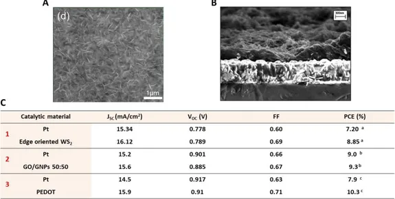
1.2.1.3 Open circuit voltage ... 17
1.2.1.4 Fill Factor, series and shunt resistances ... 17
1.2.1.5 Incident photon conversion efficiency ... 19
1.2.2 Device components ... 20
1.2.2.1 Photoelectrode ... 21
1.2.2.2 Electrolyte ... 30
1.2.2.3 Counter-electrode ... 33
1.2.3 Noble metal nanoparticles in DSSCs ... 35
1.3 Raman Scattering ... 38
1.4 Surface-enhanced Raman scattering spectroscopy ... 40
1.4.1.1 SERS enhancement mechanisms ... 41
1.4.1.2 SERS methods ... 43
1.4.1.2.1 SERS substrates: Colloidal NPs ... 44
iii
1.4.1.2.4 SERS affinity strategies ... 47
1.4.1.2.5 SERS tag strategies ... 49
1.5 Chemiresistive sensing ... 51
1.6 Heavy metals as water contaminants ... 53
2 Chapter 2 ... 56
2.1 Materials and methods ... 57
2.1.1 Materials ... 57
2.1.2 Photoanode preparation ... 57
2.1.3 Counter electrode preparation ... 58
2.1.4 Symmetrical dummy cells and DSSC assembly ... 59
2.1.5 Characterization ... 59
2.2 Results and discussions ... 62
2.2.1 Counter electrodes: morphology... 62
2.2.2 Counter electrodes: optical properties ... 65
2.2.3 Counter electrodes: catalytic activity ... 66
2.2.4 DSSCs performance ... 71
2.3 Conclusions ... 78
3 Chapter 3 ... 80
3.1 Materials and methods ... 81
3.1.1 Materials ... 81
3.1.2 Synthesis of tannic acid stabilized Ag NPs ... 81
3.1.3 Synthesis of citrate stabilized Ag NPs ... 82
3.1.4 Au NPs synthesis ... 83
3.1.5 Au@Ag core@shell NPs synthesis ... 83
3.1.6 Substrates fabrication ... 84
iv
3.1.8 Preparation of the Hg2+ solutions ... 86
3.1.9 SERS and electrical detection of Hg2+ in water and selectivity ... 86
3.1.10 Characterization ... 86
3.2 Results and discussions ... 88
3.2.1 Noble metal NPs synthesis and their optical properties in solution ... 88
3.2.2 Chemiresistive sensing platforms: fabrication and morphology ... 91
3.2.3 SERS sensing platforms optimization ... 95
3.2.4 Detection of Hg2+ ions in water ... 101
3.2.4.1 Hg2+ ions in water: chemiresistive detection and selectivity ... 101
3.2.4.2 Hg2+ ions in water: SERS detection ... 103
3.3 Conclusions ... 105
4 Appendix ... 107
5 References... 112
6 Acknowledgments ... 138
vi
List of figures
Figure 1-1 Lycurgus Cup (British Museum; IV century BC) illuminated A) from the outside and B) from the inside. C) Medieval piece of a glazed ceramic (9th century AD) observed by scattered light and specular reflection. D) TEM image of the double layer of silver nanoparticles. E) Schematic representation of interference phenomena due to the double layer with an interlayer distance of 430 nm. Adapted from references 6, 7. ... 2 Figure 1-2. Optical absorption spectra for A) Ag and B) Au NPs embedded in a silica matrix with dielectric function ε = 2.25 (diameter 40 nm). For Au NPs, the contributions to the optical absorption of interband transitions and LSPR are resolved. Adapted from Reference 8. Schematic representation of phonon-assisted C) intraband electronic transition in Ag NPs and D) interband electronic transition in Au NPs when irradiated with Vis light. Adapted from Reference 12. ... 4 Figure 1-3 TEM images of Au NPs with different shapes: A) nanospheres, B) nanocubes, C) nanorods, D) hexagons, E) nanostars. Au nanorods with different aspect ratio (the length divided by the width): F) 1-5 TEM images, G) UV-Vis spectra and H) photographs of the dispersions. Adapted from Reference 7. ... 5 Figure 1-4 A) Schematic illustration of the two possible reaction pathways for the synthesis of Au NPs as a function of the solution pH. B) Variation of the solution pH upon the addition of sodium citrate to a chloroauric acid solution (0.25 mM) and structure and reactivity of gold complexes as a function of pH. C) TEM images showing the temporal evolution of Au NPs size and shape using high (top row) and low (bottom row) citrate:HAuCl4 ratio. D) TEM images of Au NPs synthesized varying the solution pH, but with fixed initial HAuCl4 and citrate concentrations. Adapted from Reference 17. ... 6 Figure 1-5 TEM micrographs of silver colloids at A) an early stage and B) a later stage of the synthesis performed using sodium citrate as reducing and stabilizing agent. C) Temporal evolution of the absorbance of the Ag NPs plasmon band at 420 nm for different Ag+:citrate ratios. D) Schematic representation of the nucleation and primary and secondary growth of Ag NPs in the presence of citrate. Adapted from Reference 20. ... 8 Figure 1-6 A) TEM micrographs of the Au NPs after the nucleation and every growth step, with sizes ranging from ~8 to ~180 nm. B) UV-Vis spectra of the gold colloids after different growth steps. Adapted from Reference 21. ... 9 Figure 1-7 SEM images of the synthesized Ag NPs on TiO2 film at a distance of A) 15 cm, B) 20 cm, C) 25 cm from the silver source and D) Ag nanorods on TiO2 anatase, and E) Ag nanoplates on TiO2 rutile. F) Schematic representation of the growth mechanism of Ag NPs, nanorods and nanoplates on TiO2 film. Adapted from Reference 23. ... 10
vii synthesis in solution (LASiS) in aqueous solution of SDS A) 0.003 M, B) 0.01 M and C) 0.05 M. Adapted from Reference 28. ... 12 Figure 1-9. Schematic representation of the working principle of a DSSC under solar illumination. Recombination processes are indicated by dashed arrows. ... 14 Figure 1-10 Overview of the typical timescale of the main kinetic processes occurring in a DSSC. Adapted from Reference 43. ... 15 Figure 1-11 A) Hypothetical Current-Voltage (I-V) curves. Various important cell parameters are also indicated in the figure. B) Equivalent circuit for a solar cell showing the photogenerated current density Jph, the current flowing in the external load J and the applied voltage V, the series and shunt resistances, Rs and Rsh, respectively. ... 18 Figure 1-12 A) Effect of the series resistance (Rs) variation on the I-V characteristic of a solar cell, when the shunt resistance Rsh is infinite. B) Effect of the shunt resistance (Rsh) variation on the I-V characteristic of a solar cell, when the series resistance Rs is zero. Adapted from Reference 45. ... 19 Figure 1-13 Schematic representation of the processes contributing to the IPCE: light harvesting, electron injection and charge collection and their efficiencies LHE, Φinj and Φc. 20 Figure 1-14 Schematic representation of the cell components and some of the main electron transfer processes. ... 20 Figure 1-15 Comparison of the lower edge of the CB (in red), upper edge of the VB (in green) and band gap energy (in eV) for various semiconductors in contact with an aqueous electrolyte at pH 1. The standard redox potentials for some redox couples are shown, as well as the standard hydrogen potential. The energy scale is indicated in eV using both the vacuum and the normal hydrogen electrode (NHE) level as a reference. Adapted from Reference 50. ... 21 Figure 1-16 Schematic representation of A) the recombination of electrons in the FTO back contact with the oxidized form of the electrolyte and B) its suppression in the presence of the blocking underlayer... 23 Figure 1-17 Incident photon to current conversion efficiency (IPCE) as a function of the wavelength for the standard ruthenium sensitizers N3 (cis-Bis(isothiocyanato) bis(2,2’-bipyridyl-4,4’-dicarboxylato ruthenium(II), red line), the black dye N749 ([[2,2′′6′,2′′-terpyridine]-4,4′,4′′-tricarboxylato(3-)-N1,N1′,N1′′]tris(thiocyanato-N)hydrogen ruthenium(II), black curve), and the blank nanocrystalline TiO2 film (blue curve). The chemical structures of the sensitizers are shown as insets. Adapted from Reference 67. ... 24
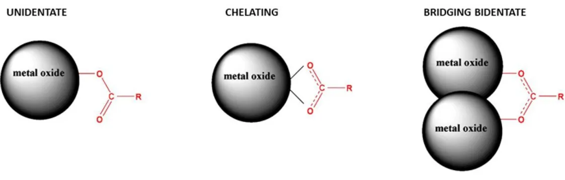
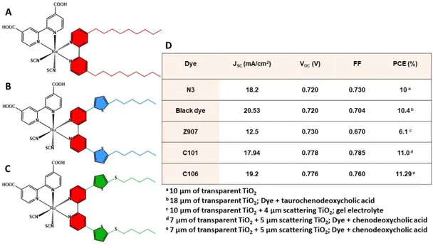
viii Figure 1-18 Binding modes of the dye through its carboxylic groups on TiO2 NPs surface. Adapted from Reference 64. ... 25 Figure 1-19 Representation of the inefficient electron injection into nanostructured metal oxide arising from aggregation and/or high degree of protonation in N3 dye. Adapted from Reference 64. ... 26 Figure 1-20 Molecular structures of A) Z907 (cis-Bis(isothiocyanato)(2,2’-bipyridyl-4,4’-dicarboxylato)(4,4’-di-nonyl-2’-bipyridyl)ruthenium(II)), B) C101 (cis-Bis(isothiocyanato)(2,2′-bipyridyl-4,4′-dicarboxylato)(4,4′-bis(5-hexylthiophen-2-yl)-2,2′ bipyridyl)ruthenium(II)), C) C106 (cis-Bis(isothiocyanato)(2,2′-bipyridyl-4,4′-dicarboxylato)( 4,4′-bis(5-(hexylthio)thiophen-2-yl)-2,2′-bipyridyl)ruthenium(II)) dyes. D) Photovoltaic performance of DSSCs equipped with N3,70 black dye,71 Z907,72 C101,73 C10674 dyes. ... 27 Figure 1-21. Active molecular orbitals (MOs) isosurfaces of the computed vertical transitions of Dye-(TiO2)15 systems at the TD-DFT/B3LYP theoretical level. The represented molecule has a triphenilamine donor, a thiophene bridge and a cyanoacrylic acid acceptor. Adapted from Reference 75. ... 28 Figure 1-22. Molecular structures of A) D35 (E)-3-(5-(4-(bis(2',4'-dibutoxy-[1,1'-biphenyl]-4-yl)amino)phenyl)thiophen-2-yl)-2-cyanoacrylic acid), B) Y123 (3-{6-{4-[bis(2',4'- dihexyloxybiphenyl-4-yl)amino-]phenyl}-4,4-dihexyl-cyclopenta-[2,1-b:3,4-b']dithiphene-2-yl}-2-cyanoacrylic acid), C) ADEKA-1 (2-Cyano-3-[5’’-(9-Ethyl-9H-carbazol-3-yl)-3,4’,4’’-tri-n-hexyl-[2,2’,5’,2’’]terthiophenyl-5- yl]trimethoxysilane, D) LEG4 (3-{6-{4-[bis(2',4'- dibutyloxybiphenyl-4-yl)amino-]phenyl}-4,4-dihexyl-cyclopenta-[2,1-b:3,4-b']dithiophene-2-yl}-2-cyanoacrylic acid). E) Photovoltaic performance of DSSCs equipped with D35,76 Y123,79 LEG4,78 ADEKA-180 dyes and ADEKA-1 + LEG438 blend. ... 29 Figure 1-23 Chemical structures of the following cobalt complexes: A) 𝐶𝑜(𝑏𝑝𝑦)3𝑛 +(bpy = 2,2’-bipyridine), B) 𝐶𝑜(𝑝ℎ𝑒𝑛)3𝑛 + (phen= 1,10-phenanthroline), C) 𝐶𝑜(𝑏𝑝𝑦 − 𝑝𝑧)3𝑛 + (bpy-pz = 6-(1H-pyrazol-1-yl)-2,2'-bipyridine). D) Reduction potentials and the photovoltaic performance of DSSCs equipped with these complexes as redox mediators.98 ... 32 Figure 1-24 SEM images of the following catalytic materials on FTO glass: A) edge oriented tungsten disulfide (WS2), B) cross-section of poly(3,4-propylenedioxythiophene) (PEDOT). C) Comparison of the photovoltaic performance of DSSCs equipped with 1) Pt and edge oriented WS2, 2) Pt and GO/GNPs 50:50 and 3) Pt and PEDOT as CEs. Adapted from References 110 and 111... 34 Figure 1-25 A) Absorption spectrum on N719 dye (in red) and LSPR bands of TiO2-Au-TiO2 (TAuT, dcore ~15 nm, dAu ~0-4 nm, dT ~2 nm) NPs (in blue), Ag@TiO2 (AgT, dcore ~15 nm, dT ~2nm) NPs (in yellow) and Au@TiO2 (AuT, dcore ~15 nm, dT ~2 nm) NPs (in purple). The
ix The scale bar represents 5 nm. C) IPCE spectra of DSSCs prepared with N719 sensitized TiO2 (in black) and with N719 sensitized TiO2 with 0.05% embedded Ag@SiO2 nanoprisms (in red). The difference spectrum is shown in blue line. D) TEM image of Ag@SiO2 nanoprisms (33 nm SiO2 shell, 70 nm total thickness) after sinterization. E) Comparison of the photovoltaic performance of DSSCs equipped with 1)TiO2 and TAuT NPs, and 2) TiO2 and TiO2 + 0.05% Ag@SiO2 as PE materials. Adapted from References 115 and 116. ... 36 Figure 1-26 A) SEM and B) TEM images of the Au NPs/rGO nanohybrid prepared by Ar plasma reduction on FTO glass and TEM grid, respectively. C) SEM image of Pt0.5Au0.5 bimetallic NPs prepared by dry plasma reduction on FTO glass. The scale bar represents 200 nm. D) Comparison of the photovoltaic performance of DSSCs equipped with 1) Pt and Au NPs/rGO nanohybrid, and 2) Pt NPs and Pt0.5Au0.5 bimetallic NPs as CE materials. Adapted from References 117 and 118. ... 37 Figure 1-27 Jablonski diagrams depicting the A) Rayleigh and B) Raman scattering processes. Alternatively, the C) Rayleigh and D) Raman scattering processes are presented showing the excitation to a virtual state, followed by the photon emission. Jablonski diagrams depicting the E) Stokes and F) anti-Stokes Raman scattering processes. G) Typical Raman spectrum of a Raman active molecule (Rhodamine 6G), showing several Raman peaks on the Stokes side and their (weaker) anti-Stokes counterparts. The spectrum was obtained using a 633 nm excitation laser line. Adapted from Reference 123. ... 39 Figure 1-28 Schematic representations of A) electromagnetic and B) chemical SERS enhancement mechanisms. Adapted from References 130and 139. ... 42 Figure 1-29 TEM images of silver A) nanospheres, B) nanorods and C) nanoprism. D) SERS spectra of Rhodamine 6G (10-3 M) with silver nanospheres, nanorods and nanoprisms obtained using a 785 nm excitation laser line. The spectra were recorded in aqueous solutions under dilute conditions, with a similar number of NPs in all the samples (~1.4 × 10¹¹/cm3). Adapted from Reference 141. ... 44 Figure 1-30 A) Extinction spectra of gold bipyramid in solution (in red) and adsorbed on paper substrate (in blue). B) SEM images of gold bipyramids adsorbed on paper substrate. In the inset, TEM image of gold bipyramids. C) SERS spectra obtained from the paper substrate adsorbed with gold bipyramids, exposed to different concentrations (5 - 0.1 nM) of trans-1,2-bis(4-pyridyl)ethane in ethanol, using a 785 nm excitation laser line. Adapted from Reference 142. ... 45 Figure 1-31 SERS spectra of bilirubin in water with concentration ranging from 10-5 M to 10– 12 M, obtained using MoS2 (black curve) and Au-MoS2 substrates, using a 633 nm excitation
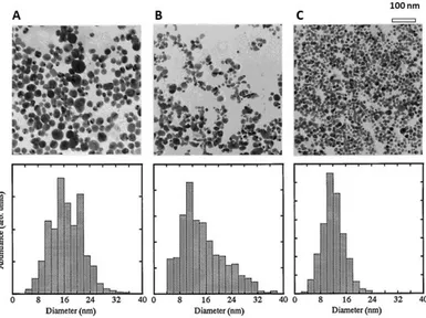
x laser line. Asterisk-marked peaks are from the MoS2. B) SEM image and C) TEM image of Au decorated MoS2 nanoflowers. The average size of Au NPs is shown in the inset. Adapted from Reference 144. ... 46 Figure 1-32 A) Schematic representation of SERS affinity strategy with unfunctionalized substrate. B) Raman and SERS spectra of pyrene at different concentrations measured at the edge of the coffee ring pattern obtained using a 785 nm excitation laser line. C) (a) SEM image and (b) EDX analysis for the coffee ring pattern (red = Na; white = Cl; yellow = Au). The middle column shows the SEM images at higher magnification, and the right column is the EDX results for five points along the diameter of the coffee ring. D) Schematic representation of SERS affinity strategy with functionalized substrate. E) Schematic representation of the Layer-by-Layer assembly of Au NPs and ammonium pillar[5]arene. F) SEM image of AuNPs/ammonium pillar[5]arene assemblies on PDDA modified glass obtained after two depositions. G) SERS spectra of pyrene at different concentrations (10 µM - 0.001 µM). H) SERS mappings obtained at 594 cm−1 with the optimized plasmonic substrate (two depositions of AuNPs/ammonium pillar[5]arene), obtained using a 785 nm excitation laser line (scale bar 20 µm). Adapted from References 146 and 147. ... 48 Figure 1-33 A) Schematic representation of the key elements in SERS tag strategy: (i) plasmonic nanoparticles, (ii) Raman reporter molecules, (iii) protective shell and (iv) target ligands. B) Schematic representation of the SERS tag strategy occurring by hot-spot turn on. C) SERS spectra of Raman reporters with different concentrations of ricin B, obtained using a 785 nm excitation laser line. Adapted from References 148, 145 and 149. ... 50 Figure 1-34. A) Schematic representation of a chemiresistor where metal NPs interconnected by a molecular linker act as active material between two electrodes. Electron tunneling or hopping occurs when a voltage (V) is applied. B) Schematic representation of the conductive film growth in the chemiresistor electrodic channel, from i) isolated NPs, passing by ii) an intermediate stage to a iii) percolated network, and the corresponding I-V curves. Adapted from Reference 150. ... 53 Figure 2-1 SEM micrographs of Pt and Au thin films deposited on FTO glass by thermal decomposition of H2PtCl6 and HAuCl4 at A-D) low and B-E) high magnification. The scale bars represent 1 μm and 500 nm at low and high magnification, respectively. Particle size distributions of the C) Pt and F) Au NPs deposited on FTO glass. ... 63 Figure 2-2 SEM micrographs of Au thin films deposited by pulsed laser ablation on A-B) c-Si substrate and D-E) FTO glass at A-D) low and B-E) high magnification. The scale bars represent 1 μm and 500 nm, at low and high magnification, respectively. Particle size distributions of the Au NPs deposited on C) c-Si substrate and F) FTO glass. ... 64
xi thermal decomposition of HAuCl4 and (red) pulsed laser ablation. B) Transmittance spectra of the (black) Pt and (blue) Au thin films deposited on FTO glass by thermal decomposition and (red) pulsed laser ablation of gold. ... 66 Figure 2-4 Square wave voltammetric measurements (reported in integral form) of Co(bpy-pz)2(PF6)3 with (black) Pt, (blue) Au therm and (red) Au PLA as working electrodes. ... 67 Figure 2-5 A) I−V curves, and B) Tafel polarization plot of the symmetrical dummy cells (0.36 cm2 active area) prepared with two identical Au PLA, Au therm and Pt CEs. ... 69 Figure 2-6 UV-Vis A) absorption spectrum of a diluted Y123 solution in ethanol (~ 0.02 mM) and B) extinction spectrum of a TiO2 photoanode (thickness 6 µm) sensitized with Y123. In the inset: schematic representation of the Y123 dye adsorbed on anatase TiO2 (101) surface and the internal charge transfer (ICT) process. ... 71 Figure 2-7 Schematic representation of the co-adsorption of Y123 dye and the de-aggregating agent, chenodeoxycholic acid (CDA), reducing the π-π stacking between the dye alkyl chains and the electron recombination with the oxidized form of the electrolyte (Ox). ... 72 Figure 2-8 Photocurrent vs Voltage for DSSCs (0.181 cm2 active area) equipped with different photoanodes: (green) 2BL 1TL 1SL, (violet) 2BL 2TL 1SL, (marine blue) 2BL 2TL 2SL. TL: transparent titania layer: SL: scattering layer. Data refer to the best performing cell for each photoelectrode. ... 73 Figure 2-9 Photocurrent vs Voltage for DSSCs (0.181 cm2 active area) equipped with different counter electrodes: (black) Pt, (blue) Au therm and (red) Au PLA. Data refer to the best performing cell for each CE. ... 76 Figure 3-1 Schematic representation of the electrostatic layer-by-layer (LbL) deposition of polyelectrolytes and TA stabilized Ag NPs on glass substrate. ... 85 Figure 3-2 UV-Vis-NIR extinction spectrum of the synthesized citrate stabilized Ag NPs dispersed in water. ... 88 Figure 3-3 A) UV-Vis-NIR extinction spectra of the synthesized tannic acid stabilized Ag NPs dispersed in water, with sizes ranging from 15 to 125 nm. B) UV-Vis-NIR extinction spectra of tannic acid stabilized Ag seeds (15 nm) and 100 nm Ag NPs after centrifugation. The blue and green lines indicate the position of the dipolar and quadrupolar bands, respectively for 100 nm Ag NPs. ... 89 Figure 3-4 UV-Vis-NIR spectra of the synthesized Au NPs dispersed in water, with sizes ranging from 18 to 54 nm... 90
xii Figure 3-5 UV-Vis-NIR spectra of the synthesized A) 32 nm Au@Ag core@shell NPs, starting from a 22 nm Au core (black spectrum) and B) 110 nm Au@Ag core@shell NPs, starting from a 54 nm Au core (black spectrum), dispersed in water. ... 91 Figure 3-6 SEM images of the TEG-citrate stabilized Ag NPs network on chemiresistive substrates exposing gold IDEs (L= 2.5 µm) at A) low and B) high magnification, showing the formation of nanoparticles, nanorods and triangular nanoplates. The scale bars represent 5 and 1 µm, respectively. ... 92 Figure 3-7 A) SEM images of the APTES-tannic acid stabilized Ag NPs network and B) APTES-Ag NPs-(TEG-Ag NPs)3 on chemiresistive substrates exposing gold IDEs (L= 2.5 µm). The scale bars represent 10 µm. ... 93 Figure 3-8 SEM images of the Au@Ag NPs network on APTES functionalized chemiresistive substrates exposing gold IDEs (L= 2.5 µm) with A) 32 nm and B) 110 nm core@shell NPs. The scale bar represents 1 and 100 µm, respectively. ... 94 Figure 3-9 SEM images of the PDDA-TA stabilized Ag NPs network, obtained after 3 consecutive depositions on chemiresistive substrates exposing gold IDEs (L= 2.5 µm). Ag NPs size is 37 nm. The inset image shows the highlighted region at a higher magnification. The scale bars represent 10 µm and 3 µm in the low and high magnification image, respectively. ... 94 Figure 3-10 SEM images of the plasmonic thin films obtained after A) one, B) two, C) three, D) four and E) five LbL depositions of PDDA and 37 nm Ag NP on glass substrates. The scale bar represents 1 µm. ... 95 Figure 3-11 AFM images (resolved by 512×512 pixels) and line trace along the dashed lines of the plasmonic thin films obtained after A) one, B) two, C) three and D) four LbL depositions of PDDA and 37 nm Ag NP on glass substrates. The insets are resolved by 1024x1024 pixels. The scale bars represent 1 µm and 200 nm in the main images and the insets, respectively. ... 96 Figure 3-12 A) UV-Vis-NIR extinction spectra of the plasmonic sensing platforms prepared by (blue) one, (yellow) two, (green) three, (red) four and (grey) five consecutive LbL depositions of PDDA and TA acid stabilized Ag NPs (37 nm diameter) on glass substrate. The position of the Raman laser line is highlighted in violet. B) Stability over 15 days of the UV-Vis-NIR extinction spectra of a plasmonic sensing platform prepared with three LbL depositions of PDDA and TA acid stabilized Ag NPs (37 nm diameter) on glass substrate, after NaBH4 treatment. ... 97 Figure 3-13 A) Average SERS spectrum of 1-naphthalenthiol (1-NAT) adsorbed on a plasmonic sensing platform prepared by 3 LbL depositions of PDDA and 37 nm Ag NPs.
xiii ring stretching band (1367 cm-1) as a function of the Ag NPS size and number of depositions. SERS mappings of the SERS intensity of the 1367 cm-1 band on the plasmonic sensing platforms prepared by 3 LbL depositions of PDDA and Ag NPs with a diameter of C) 15 nm, D) 23 nm, E) 37 nm and F) 43 nm. The scale bar represents 10 µm, while the colour scale refers to the maximum SERS intensity obtained with 3 depositions of 37 nm Ag NPs. ... 99 Figure 3-14 A) SERS intensity of 1-NAT ring stretching band (1367 cm-1) as a function of the number of depositions of 37 nm Ag NPs. SERS mappings obtained at 1367 cm-1 after B) one, C) two, D) three, E) four and F) five depositions of PDDA and 37 nm Ag NPs. The scale bar represents 10 µm, while the colour scale refers to the maximum SERS intensity obtained after 3 depositions. ... 100 Figure 3-15 A) Current-Voltage curves for the chemiresistive substrates functionalized with 3 LbL depositions of PDDA and 37 nm Ag NPs (red) before and (black) after the immersion in 1 mM Hg(NO3)2 solution for 30 min. B-C) SEM micrographs of the plasmonic thin films deposited on chemiresistive substrates B) before and C) after the immersion in 1 mM Hg(NO3)2 solution for 30 min. The electrodic channel length is 2.5 µm and the scale bars represent 3 µm. D) Current-Voltage curves for the chemiresistive substrates functionalized with 3 LbL depositions of PDDA and 37 nm Ag NPs before and after the immersion in 1 mM salt solutions for 30 min. The reported I-V curves are the average of four different acquisitions. E) Resistance ratio (final resistance Rf / initial resistance Ri) for the plasmon modified chemiresistive substrates extrapolated from the I-V curves as a function of the metal ions. ... 102 Figure 3-16 A) Average SERS spectra of TA capping agent on 37 nm Ag NPs (black) before and (green) after the immersion in Hg(NO3)2 1 mM for 30 min. The sensing platform was prepared by 3 LbL depositions of PDDA and 37 nm Ag NPs. B-C) SERS mappings obtained at 1300 cm-1 B) before and C) after the immersion of the sensing platform in Hg(NO3)2 1 mM for 30 min. D) Variation of the 1-NAT 1367 cm-1 peak area ratio (Af/Ai) with the immersion in Hg(NO3)2 1 µM for 1, 5 and 30 min. E-F) SERS mappings obtained at 1367 cm-1 E) before and F) after the immersion of the sensing platform in Hg(NO3)2 1 µM for 1 min. The scale bars represent 10 µm. ... 104 Figure 4-1 A-D) STEM images of the synthesized tannic acid stabilized Ag NPs. The reported sizes were determined as an average of the diameter of 100 particles for each Ag NPs generation. E-H) Particle size distribution for every Ag NPs generation. ... 107 Figure 4-2 UV-Vis-NIR extinction spectra of the plasmonic sensing platforms prepared by (blue) one, (yellow) two, (green) three and (red) four LbL depositions of PDDA and TA acid
xiv stabilized Ag NPs with the following diameter: A) 15 nm, B) 23 nm and C) 43 nm on glass substrate. The position of the Raman laser line is highlighted in violet ... 107 Figure 4-3 Average SERS spectra of 1-NAT adsorbed on a sensing platform was prepared by 3 LbL depositions of PDDA and 37 nm Ag NPs (black) before and after the immersion in in Hg(NO3)2 1 µM for (red) 1 min, (blue) 5 min and (green) 30 min. The ring stretching band (1367 cm-1) is highlighted in blue. ... 110
NP Nanoparticles
PLD Pulsed laser deposition DSSC Dye-sensitized solar cell PCE Power conversion efficiency PE Photoelectrode
CE Counter electrode
TCO Transparent conductive oxide ITO Indium tin oxide
FTO Fluorine-doped tin oxide
HOMO Highest occupied molecular orbital LUMO Lowest unoccupied molecular orbital
N3 cis-bis(isothiocyanato)bis(2,2’-bipyridyl-4,4’-dicarboxylato ruthenium(II)
N719 Di-tetrabutylammonium-cis-bis(isothiocyanato)bis(2,2’-bipyridyl-4,4’-dicarboxylato)ruthenium(II) Z907 cis-Bis(isothiocyanato)(2,2’-bipyridyl-4,4’-dicarboxylato)(4,4’-di-nonyl-2’-bipyridyl)ruthenium(II) FoM Figure of merit
Jsc Short-circuit current Voc Open circuit voltage FF Fill factor
η (PCE) solar-to-electric power conversion efficiency PV photovoltaic
EQE external quantum efficiency
IPCE incident photon conversion efficiency
λ wavelength
HTM Hole transporting material ICT Internal charge transfer D-π-A Donor-π bridge-Acceptor
CB Conduction band
ACN acetonitrile VN valeronitrile
MPN 3-methoxypropionitrile TBP 4-tert-butylpyridine
CVD Chemical vapour deposition
GR graphene
PEDOT poly(3,4-propylenedioxythiophene) LH Light harvesting
xvi
Eg Energy band gap
µe Electron mobility
LASiS Laser ablation synthesis in solution SDS sodium dodecyl sulfate
PLD or PLA Pulsed laser deposition or ablation LSP Localized surface plasmon
LSPR Localized surface plasmon resonance EM electromagnetic
Ε Dielectric function
SERS Surface enhanced Raman spectroscopy
CM chemical
LbL Layer-by-Layer BL Blocking layer
TL Transparent titania layer SL Scattering layer
D Diffusion coefficient Jlim Limiting current density
RS Series resistance
RSh Shunt resistance
TA Tannic acid
SC Sodium citrate
xviii
Abstract
The aim of this thesis is to assess the possible applications of noble metal nanoparticles (NPs) in the fields of solar energy production and chemical sensing. The research project arises directly from the well-known extraordinary properties of noble metal NPs, namely the optical and electrical properties, high surface area, high catalytic activity and surface enhanced Raman scattering effect.
More specifically, concerning the energy production field, the first part of the thesis will deal with the application of Au NPs as counter electrode material in dye sensitized solar cells (DSSCs). This study was conducted in the S.O.L.A.R.E. laboratory at the Istituto per i Processi Chimico-Fisici of the Italian National Research Council (IPCF-CNR) in Messina, under the supervision of Dr. Giuseppe Calogero.
To the best of our knowledge, the role of noble metal NPs as exclusive counter electrode material in DSSCs has not been explored yet, despite their catalytic activity (i.e. applications in water purification) and electron conductivity have been massively studied. On the other hand, gold mirror thin films were used in combination with graphene nanoplatelets for the fabrication of the counter electrode in the most efficient DSSC reported in literature. For this reason, the work conducted towards the realisation of this thesis has been focused on the development of an efficient and reproducible method for the fabrication of Au based counter electrodes for DSSCs. Two different methods have been proposed, namely the thermal decomposition of HAuCl4 as bottom-up method and the pulsed laser ablation of a gold target
as top-down method. They were compared on the basis of the counter-electrodes optical properties, surface morphology, catalytic activity and performance both in dummy cells and fully assembled DSSCs. In the latter case, the adequate photoanode configuration has been studied, in order to
xix conversion efficiency. In addition, the fabricated gold counter-electrodes were compared to standard platinum ones.
In the second part of the thesis, the use of Ag NPs for the fabrication of multiresponsive plasmonic sensing platforms for surface enhanced Raman scattering (SERS) and chemiresistive sensing will be presented. This work has been conducted in the Nanochimie laboratory at the Institut de Science et d'Ingénierie Supramoléculaires (ISIS) in Strasbourg, under the supervision of Prof. Paolo Samorì.
The development of SERS based sensors has experienced an enormous growth in the last decades, as a consequence of their high versatility, high sensitivity, ease of fabrication and low cost. However, despite the inherently higher SERS activity of Ag compared to Au, sensing platforms based on Au NPs are already commercially available, while Ag NPs are mainly employed as colloidal dispersions, due to their lower chemical stability arising from oxidation. On the other hand, the extraordinary electrical properties of noble metal NPs made them suitable as active conductive materials in chemiresistors. Within this context, different synthetic procedures have been used to obtain citrate stabilized Ag NPs, tannic acid stabilized Ag NPs and Au@Ag core@shell NPs. Besides the study of their optical properties in colloidal solutions, they were compared by means of their ability to give rise to uniform thin films on chemiresistive devices, using both the cross-linking with dithiols and the electrostatic layer-by-layer deposition. The best results were obtained with the electrostatic layer-by-layer deposition of tannic acid stabilized Ag NPs, so that the optical properties, surface morphology, SERS and chemiresistive activity of these devices was largely studied. Furthermore, the possibility to use the fabricated sensing platforms for the
xx sensing of mercury ions in water by both indirect SERS and resistance variation was explored.
1
1 Introduction
1.1 Noble metal nanoparticles
Since their first use as decorative pigments, noble metal nanoparticles (NPs) demonstrated to have very unique and fascinating properties. Nowadays, it is still possible to admire the Lycurgus cup, dated IV century BC, whose unique optical properties can be ascribed to the presence in the glass matrix of small metal crystals containing Ag and Au with a molar ratio of about 14:1 and a diameter of ~70 nm. For this reason, the glass cup appears green when illuminated from the outside and observed in reflected light (Figure 1-1A), while it looks ruby red when the light comes from the inside and is transmitted through the glass (Figure 1-1B).1 The Romans were thus able to
use colloidal NPs to represent Lycurgus myth: in the Iliad, Homer depicts Lycurgus as a strong, mighty king, who was punished with blindness when he dared to challenge “mad Bacchus”, heavenly God of grape-harvest and wine.2 However, the famous cup represents another version of the myth,
showing Lycurgus being tangled up by the Greek nymph and disciple of Bacchus, Ambrosia, who is disguised as a vine.3 The synthetic route used by
the Romans is not clear yet, but several studies conducted on the Lycurgus cup suggest that the simultaneous presence of silver, gold, copper and antimony in the soda-lime-silica glass matrix and the heat treatment could have caused the precipitation of a fine dispersion of Ag-Au alloy NPs.4, 5
Later on, in Mesopotamia during the 9th century AD, silver and/or copper NPs
were dispersed within the outermost layers of glazed ceramics to obtain metallic luster decorations: for example, the medieval glaze in Figure 1-1C shows iridescence under specular reflection, with shiny blue and green colours. When transmission electron microscopy (TEM) analysis is
2
performed on the sample, a double layer of silver nanoparticles with sm aller sizes (5–10 nm) in the outer layer and larger ones (5–20 nm) in the inner layer can be observed (Figure 1-1D). A schematic representation of the interference between the two layers with constant distance of about 430 nm is shown in Figure 1-1E. The light scattered by the second layer has a phase shift with respect to the one scattered by the first layer: each wavelength is scattered differently, since the phase shift depends on the wavelength of the incoming light.6, 7
Figure 1-1 Lycurgus Cup (British Museum; IV century BC) illuminated A) from the outside and B) from the inside. C) Medieval piece of a glazed ceramic (9th century AD) observed by scattered light and specular reflection. D) TEM image of the double layer of silver nanoparticles. E) Schematic representation of interference phenomena due to the double layer with an interlayer distance of 430 nm. Adapted from references 6, 7.
1.1.1 Optical properties of noble metal nanoparticles
The beautiful examples reported in the previous Section suggest that noble metal NPs are characterized by extraordinary optical properties, that make them suitable for a high number of applications. The optical properties are
3 exploited when light interacts with matter, thus an exact analysis can be obtained solving the Maxwell equations with the appropriate boundary conditions. However, this goes beyond the scope of this thesis. More classically, when a NP is illuminated, the electromagnetic (EM) field of light interacts with the conduction electrons, which usually move freely inside the particle creating the so-called plasmon. As a consequence, an electric dipole is created, so that negative and positive charges accumulate in opposite regions in the particle and the generated electric field results opposite to the light one. Since the size of the NP is much smaller than the photon wavelength, the resulting plasmon oscillation is distributed over the whole particle volume, hence localized surface plasmons (LSPs) are created. The electrons displacement generates a restoring force, so that when the external field is removed, they oscillate with a resonant plasmon frequency.8, 9
Consequently, a resonance is achieved as soon as the frequency of the EM radiation approaches the LSP frequency, so that a localized surface plasmon resonance (LSPR) band can be observed in the extinction spectrum of the NPs colloid.10 The extinction cross-section for metallic NPs, which depends
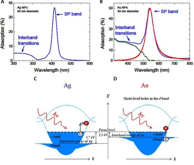
also on the power of the incident light, is the summation of the absorption and scattering contributions and it is defined as the effective area of a homogeneous incoming beam from which they will absorb or scatter every photon. Additionally, LSPR is strongly dependent on the NP size or shape, the dielectric function of the surrounding medium and the nature of the metal. In Figure 1-2A-B, it is possible to notice that two kinds of transitions are excited when Ag and Au NPs are illuminated. Apart from the LSPR, interband transitions have a certain probability to take place. In the case of silver, the two bands are well-resolved, since the interband energy is quite high (Figure 1-2C) and this behaviour can be described with a lossless Drude model.11 A
4 shown in Figure 1-2D, the interband energy is small, so that losses, associated to the transition between d levels and the conduction band, are likely: interband transitions and LSPR overlap, resulting in the decay into electron-hole pairs and a reduced plasmon intensity.8, 9, 12 However, although
Ag outperforms Au, usually Au is preferred due to its higher chemical stability and biocompatibility in most applications.
Figure 1-2. Optical absorption spectra for A) Ag and B) Au NPs embedded in a silica matrix with dielectric function ε = 2.25 (diameter 40 nm). For Au NPs, the contributions to the optical absorption of interband transitions and LSPR are resolved. Adapted from Reference 8.
Schematic representation of phonon-assisted C) intraband electronic transition in Ag NPs and D) interband electronic transition in Au NPs when irradiated with Vis light. Adapted from Reference 12.
The optical properties of noble metal NPs are influenced not only by the nature of the metal, but also by the size and shape of the particles. Adjusting the synthetic procedure, various morphologies can be obtained, spanning from nanospheres to nanocubes, hexagonal shapes, nanorods and nanostars (Figure 1-3). Interestingly, all these NPs have different optical properties. For example, in the case of gold nanorods with different aspect ratios (the length divided by the width), this effect is visible to the naked eye.
5 The UV-Vis spectra for gold nanorods typically show two bands: one at higher energy, corresponding to the collective oscillation of free electrons in the presence of the external EM field along the transverse dimension, and the other at longer wavelengths, corresponding to the absorption and scattering of light along the longitudinal dimension of the nanorod.13 As the
length of the rod increases, it is possible to observe a shift of the band at longer wavelengths, from the visible to near infrared, and the colour of the corresponding dispersions changes from pink to blue, green and brownish (Figure 1-3F-H).7
Figure 1-3 TEM images of Au NPs with different shapes: A) nanospheres, B) nanocubes, C) nanorods, D) hexagons, E) nanostars. Au nanorods with different aspect ratio (the length divided by the width): F) 1-5 TEM images, G) UV-Vis spectra and H) photographs of the dispersions. Adapted from Reference 7.
Nowadays, numerous strategies for the synthesis of noble metal NPs have been reported in literature, but they can be mainly divided in two macro-groups, namely bottom-up and top-down methods. The former deals with the
6 reaction of atoms or molecules under specific chemical or physical conditions, while the latter is essentially the reduction in NPs of bulk materials by means of physical, mechanical or chemical processes.14
1.1.2 Bottom-up synthesis of noble metal nanoparticles
The chemical reduction of precursors is one of the most common methods for the synthesis of noble metal NPs. Apart from the precursor, two species are fundamental for the synthesis, namely the reducing agent and the stabilizer, and two steps are essential, namely the nucleation and the growth. In 1951 Turkevich reported the in situ synthesis of Au NPs with a size of 20 nm from the reduction of chloroauric acid (HAuCl4) in boiling water containing
sodium citrate as stabilizing and reducing agent.15 The method was later
improved by Frens, who found that Au NPs with sizes ranging from 15 to 150 nm can be obtained adjusting the HAuCl4 : citrate ratio.16
Figure 1-4 A) Schematic illustration of the two possible reaction pathways for the synthesis of Au NPs as a function of the solution pH. B) Variation of the solution pH upon the addition of sodium citrate to a chloroauric acid solution (0.25 mM) and structure and reactivity of gold
7
complexes as a function of pH. C) TEM images showing the temporal evolution of Au NPs size and shape using high (top row) and low (bottom row) citrate:HAuCl4 ratio. D) TEM images of Au NPs synthesized varying the solution pH, but with fixed initial HAuCl4 and citrate concentrations. Adapted from Reference 17.
Here, nucleation and growth take place in the same process, and the size distribution is determined by various parameters, such as temperature, pH and strength of the reducing and stabilizing agents. Since citrate is a weak base, changing its concentration, the solution pH is also changing. Furthermore, the reactivity of gold complexes, reflected by their reduction potentials, varies markedly when the pH changes (Figure 1-4B). As shown in Figure 1-4A, Ji et al. found that two different reaction pathways are followed when the synthesis is carried out at low and high pH values. Under high pH (6.5-7.7), which correspond to a high citrate: chloroauric acid ratio, nucleation is quite slow (~ 60 sec) and it is followed by slow diffusion-controlled growth, giving rise to relatively small NPs. When the pH is lower (3.7-6.5), the higher reactivity of the formed gold complexes is accompanied by a faster nucleation, followed by random attachment and intra-particle ripening, giving rise to relatively larger NPs with higher polydispersity. The TEM images showing the temporal size and shape evolution of Au NPs as a function of citrate: HAuCl4 ratio and pH are shown in Figure 1-4 C-D.17
Other common in situ synthesis of Au NPs are carried out using different stabilizing agents, such as borohydride, hydrazine, formaldehyde, hydroxylamine, citric and oxalic acid, polyols, hydrogen peroxide etc., or stabilizing agents, such as thiolates, phosphorus-, nitrogen-, oxygen-based ligands, dendrimers, polymers and surfactants (i.e. cetyltrimethylammonium bromide, CTAB).18
When the Turkevich method is applied to the synthesis of Ag NPs starting from AgNO3, the ability of citrate to form relatively stable complexes with
positively charged silver ions, leads to the formation of relatively big and polydisperse Ag NPs (30-150 nm) and a variety of shapes, such as spheres,
8 rods, plates and polyhedra.19 Pillai et al. showed how citrate is able to
influence the particles growth and morphology. The augmented absorbance of the broad plasmon band at 420 nm with time is a clear sign of a slow particle growth, whose rate is also influenced by citrate concentration. (Figure 1-5C) The TEM images in Figure 1-5A-B show that small spherical Ag NPs are formed in the early stage of the reaction, but the presence of citrate induces their agglomeration into nanoclusters, until an optimal size. However, the small particles undergo the so-called Ostwald ripening process: they are reoxidized to Ag+ ions and then adsorbed on the surface
of bigger particles, where they are reduced. A complete scheme of the nucleation and primary and secondary growth of Ag NPs in the presence of citrate is shown in Figure 1-5D.20
Figure 1-5 TEM micrographs of silver colloids at A) an early stage and B) a later stage of the synthesis performed using sodium citrate as reducing and stabilizing agent. C) Temporal evolution of the absorbance of the Ag NPs plasmon band at 420 nm for different Ag+:citrate ratios. D) Schematic representation of the nucleation and primary and secondary growth of Ag NPs in the presence of citrate. Adapted from Reference 20.
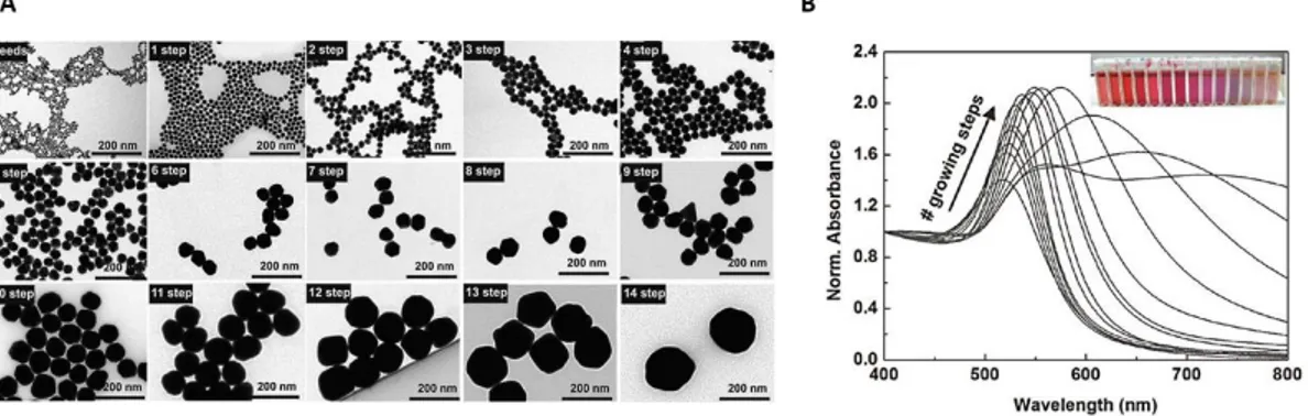
9 More recently, aiming to obtain better size and shape control of the NPs, seeded-growth methods have been developed, based on the temporal separation of nucleation and growth. Bastús et al. proposed this method for the synthesis of highly monodisperse Au NPs: the nucleation occurs in boiling water in the presence of sodium citrate, thus producing small seeds (~8 nm). Later, seeds growth is performed thanks to the accurate control of temperature and number of Au atoms added in every growth step. Indeed, after the synthesis of Au seeds, the subsequent steps were carried at 90°C in order to favour growth against secondary nucleation and, besides, avoid the Ostwald ripening process. The TEM images in Figure 1-6A show the step by step increase in the size of Au NPs after every growth step (from ~8 to ~180 nm). The UV-Vis spectra of the gold colloids in Figure 1-6B exhibit a well-defined LSPR band, which is peaked at 518 nm for the Au seeds, while it is red shifted at every growth step; furthermore, the increasing absorbance is a proof of the deposition of Au on the preformed seeds.21
Figure 1-6 A) TEM micrographs of the Au NPs after the nucleation and every growth step, with sizes ranging from ~8 to ~180 nm. B) UV-Vis spectra of the gold colloids after different growth steps. Adapted from Reference 21.
Unlike the above-mentioned solution processed bottom-up methods, a direct synthesis method of noble metal NPs is the thermal decomposition of solid
10 precursors, which is useful for the production of large amounts of material, but, on the other hand, appears to be a complex process, due to the high number of factors affecting the solid-state and solid-gas systems. Thus, suitable precursors, heating rate, annealing time, temperature and atmosphere should be carefully selected and controlled.22 Wang et al.
succeeded in the synthesis of Ag NPs from the thermal decomposition of silver nitrate in a chemical vapour deposition system with a source temperature of 400°C, while the substrate temperature varies in the range 110-350°C. Ag NPs were synthesized on TiO2 films. The authors observed
that the particles size decreases from 75 to 25 nm when the distance from the silver source, which is directly proportional to the decreased substrate temperature, varies from 15 to 25 cm. Furthermore, when different values of pressure are applied on TiO2 anatase or rutile, nanorods or nanoplates are
formed, respectively. SEM images of the obtained Ag nanostructures and a schematic representation of the synthetic procedure are shown in Figure 1-7A-F.23
Figure 1-7 SEM images of the synthesized Ag NPs on TiO2 film at a distance of A) 15 cm, B) 20 cm, C) 25 cm from the silver source and D) Ag nanorods on TiO2 anatase, and E) Ag nanoplates on TiO2 rutile. F) Schematic representation of the growth mechanism of Ag NPs, nanorods and nanoplates on TiO2 film. Adapted from Reference 23.
11 Similarly, the thermal decomposition of precursor salts dissolved in organic solvents is particularly suitable for the direct formation of NPs on the desired substrate surface, for various technological applications, as it will be shown later in this thesis.24
1.1.3 Top-down synthesis of noble metal nanoparticles
An effective technique for the preparation of noble metal NPs is the laser ablation synthesis in solution (LASiS), which relies on the pulsed laser irradiation of a bulk metal source dipped in a liquid solution. Although a comprehensive explanation of the synthetic procedure is still lacking, it has been established that photons are absorbed in the irradiated area of the metal source, thus causing heating and photoionization, which give rise to the expulsion of material generating an expanding plasma plume. Supersaturation in the plasma plume is the major driving force for the nucleation of NPs, which is followed by diffusion-limited growth and coalescence, also favoured by the cooling effect of the surrounding liquid. The size distribution and morphology of the particles can be influenced by various factors, such as the nature of the solvent and the presence of electrolytes or surfactants.25, 26 Tilaki et al. studied the laser ablation of
copper in deionized water and acetone and noticed that in the first case the obtained particles observed with TEM are characterized by an average size of 30 ± 14 nm and have a core@shell structure, which can be ascribed to the presence of a Cu core and a CuO shell. Furthermore, the diffraction pattern of the obtained particles confirms this observation. On the other hand, when the ablation is performed in acetone, the particles, all appearing in the same contrast, have an average size of 3 ± 1.3 nm and the diffraction pattern is the typical one for Cu NPs. These findings clearly suggest that water has a role
12 in the surface oxidation of the obtained particles, while acetone works as a capping layer on the NPs surface, thus preventing oxidation.27 Although one
of the main advantages of LASiS is the possibility to synthesize uncapped naked NPs in solution, it was demonstrated that the absence of a capping agent is the reason for the formation of big NPs aggregates, which are also prone to precipitation. Mafuné et al. studied the influence of sodium dodecyl sulfate (SDS) on the ablation of Ag in water and found that the average diameter of Ag NPs decreases as the SDS concentration increases.28 (Figure
1-8A-C)
Figure 1-8 TEM micrographs and size distribution of Ag NPs prepared by laser ablation synthesis in solution (LASiS) in aqueous solution of SDS A) 0.003 M, B) 0.01 M and C) 0.05 M. Adapted from Reference 28.
LASiS revealed to be a feasible method for the synthesis of ligand-free AuAg bimetallic NPs: Ag is ablated in a gold colloidal solution and the composition and the optical properties, consequently, strongly vary with the initial Au NPs concentration.29, 30
The laser-metal target interaction can take place also in a different environment, such as in vacuum or in the presence of a background gas. In
13 these cases, pulsed laser deposition or ablation (PLD or PLA) is a useful technique for the deposition of nanostructured thin films, as it will be shown later in this thesis.
1.2 Dye-sensitized solar cells
Dye-sensitized solar cells (DSSCs), along with perovskite solar cells, can be considered the most promising alternatives to conventional Si-based or thin film solar cells, being able to convert solar energy to electricity with acceptable efficiency and moderate costs.31, 32
DSSCs appeared in literature in 1991 for the first time, when Grätzel and O’Regan proposed a low cost and highly efficient solar cell,33 based on light
harvesting by a sensitizing dye attached to a wide band gap semiconductor.34–37
State-of-the-art DSSCs based on iodide/triiodide or cobalt based redox couples in a liquid electrolyte reached validated power conversion efficiencies (η or PCE) of 14%,38 while, when a solid-state hole conductor is
used, PCE can reach values over 5%.39 Nowadays, several companies are
able to manufacture DSSCs for residential installations as well as consumer electronics.
A typical DSSC can be schematized as a photoanode or photoelectrode (PE), constituted by a dye adsorbed on a n-type semiconductor oxide (typically TiO2 in the anatase phase), in contact with a hole transporting
material (HTM), such as a liquid electrolyte. The flow of charges in the system is ensured by the presence of a catalytic material on the counter-electrode (CE) surface. Both the PE and the CE are made of conducting glass, prepared covering the glass with a transparent conducting oxide (TCO), typically indium tin oxide (ITO) or fluorine-doped tin oxide (FTO).33, 40, 41 The
14 working principle of a DSSC under solar illumination is presented in Figure 1-9.
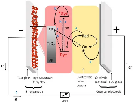
Figure 1-9. Schematic representation of the working principle of a DSSC under solar illumination. Recombination processes are indicated by dashed arrows.
𝐷𝑦𝑒 + ℎ𝜈 → ∗𝐷𝑦𝑒 ( a ∗𝐷𝑦𝑒 → 𝐷𝑦𝑒+ + 𝑒 𝑐𝑏−(𝑇𝑖𝑂2) ( b 𝑂𝑥 + 𝑒−(𝑐𝑎𝑡ℎ𝑜𝑑𝑒) → 𝑅𝑒𝑑 (𝑐𝑎𝑡ℎ𝑜𝑑𝑒) ( c 𝐷𝑦𝑒+ + 𝑅𝑒𝑑 → 𝐷𝑦𝑒 + 𝑂𝑥 ( d 𝑂𝑥 + 𝑒𝑐𝑏−(𝑇𝑖𝑂2) → 𝑅𝑒𝑑 + 𝑇𝑖𝑂2 ( e 𝐷𝑦𝑒 + +𝑒𝑐𝑏−(𝑇𝑖𝑂2) → 𝐷𝑦𝑒 + 𝑇𝑖𝑂2 ( f ∗𝐷𝑦𝑒 → 𝐷𝑦𝑒 + ℎ𝜈’ 𝑜𝑟 𝛥 ( g
Upon irradiation, (a) photon absorption gives place to the excitation of electrons from the dye Highest Occupied Molecular Orbital (HOMO) to its Lowest Unoccupied Molecular Orbital (LUMO), thus leading to the formation of *Dye, (b) which is then able to inject charges from the LUMO in the conduction band of the TiO2 semiconductor. Here, electrons firstly diffuse in
15 the disordered TiO2 network until they reach the back contact of the anode
and then (c) to the CE, through the external circuit. Simultaneously, (d) thanks to the presence of a catalytic material on the CE surface, reduction of Ox (oxidized form of the electrolyte) occurs, while (e) Dye+ (oxidized dye)
rapidly transfers its holes to Red, the electron rich form of the redox couple. A good dye regeneration is ensured when the energy of the HOMO of the redox mediator is higher than the dye one. However, the electron transfer events here described can be limited by several undesirable loss reactions, such as the charge recombination from the semiconductor conduction band (f) to Dye+ which gives rise to the so-called dark current, or (g) to Ox
(recombination back reaction), and (h) the (radiative or non-radiative) decay of the LUMO level of the dye to its HOMO one.42 The typical time constants
for the described processes are shown in Figure 1-10.
Figure 1-10 Overview of the typical timescale of the main kinetic processes occurring in a DSSC. Adapted from Reference 43.
Since their first appearance in literature, researchers have worked on the optimization of all the components of DSSCs, in order to maximize the cell performances. However, before reviewing the recent advances in the field, the device key parameters and figures of merit (FoM) should be presented.
16
1.2.1 Key parameters and figures of merit
1.2.1.1 Photoconversion efficiency
The photoconversion efficiency (PCE) of a solar cell is given by the ratio between the maximum generated power (Pmax) and the power of the incident
light (Pin) and it is usually calculated by the following equation:
𝜂 = 𝑃𝑚𝑎𝑥 𝑃𝑖𝑛 = 𝐽𝑚𝑎𝑥 ∙ 𝑉𝑚𝑎𝑥 𝑃𝑖𝑛 = 𝐽𝑆𝐶∙ 𝑉𝑂𝐶∙ 𝐹𝐹 𝑃𝑖𝑛
The key parameters are the photocurrent and photopotential which can be experimentally measured under different conditions, such as open or short circuit and under monochromatic or sunlight illumination.
1.2.1.2 Short circuit density
The short circuit density (Jsc) is the highest current density that a cell can
supply at 1 sun when it is short-circuited. The Jsc is closely related to the
ability of the dye to absorb light over a wide range of wavelengths and to inject electrons from its excited level to the semiconductor conduction band (Eqn (a, Eqn (b). Furthermore, higher is the rate of dye regeneration (Eqn (d) ensuring low values of dark current (Eqn (f), higher is the Jsc. Indeed, the
overall Jsc is given by the following equation:
𝐽𝑆𝐶 = 𝐽𝑖𝑛𝑗− 𝐽𝑟𝑒𝑐
Where Jinj represents the injection current, while Jrec is the recombination
current contributing to the photovoltaic (PV) performance loss. In particular, JSC is closely related to the light harvesting efficiency (LHE), the charge
17 injection and charge collection efficiencies,44 which will be presented in
Section 1.2.1.5.
1.2.1.3 Open circuit voltage
Another key parameter which can be highly affected by the recombination processes is the open circuit voltage (Voc): it represents the electrical
potential difference when no current is flowing between PE and CE under illumination. The maximum Voc for a DSSC is given by the difference between
the quasi-Fermi energy level for the semiconductor (Ecb) and the redox
potential of the electrolytic couple (Ered). Nevertheless, a more complete
description of the Voc is given by the following equation:
𝑉𝑂𝐶 =𝑘𝑇 𝑞 ln (
𝜂Φ0
𝑛0𝑘𝐸𝑇[𝑂𝑥])
Where k is the Boltzmann constant, T is the absolute temperature, q is unit charge; η and Φ0 are closely related to the Jinj and they represent the
photogenerated electrons quantum yield and the incident photon flux, respectively. The influence of the loss reactions is given by the terms n0, kET
and [Ox] which are the electron density in the semiconductor conduction band in the dark, the recombination rate constant and the concentration of the oxidized form of the electrolyte, respectively.45
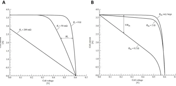
1.2.1.4 Fill Factor, series and shunt resistances
The fill factor (FF) is a measure of the quality of the cell, since it is given by the ratio between the maximum theoretical power (𝑃𝑚𝑎𝑥 = 𝐽𝑚𝑎𝑥 ∙ 𝑉𝑚𝑎𝑥) and the real output power (𝑃𝑜𝑢𝑡 = 𝐽𝑆𝐶∙ 𝑉𝑂𝐶). It is calculated as the ratio between
18 represents the easiness of extraction of the photo-generated charge carriers from the solar cell. The FF can assume values in the range 0-1. Indeed, if we consider the Voc as the illumination dependent resting potential of the cell,
the FF value will differ from unity as the Voc faces voltage losses; the latter
are caused by the presence of internal resistances when an external load is connected and the current starts to flow.46 The FF can be affected by the
series resistance (RS) and the shunt resistance (Rsh): the former can be
associated to the bulk resistance of the materials and the electrodes, the contact resistance at the interface between the various cell components and charge transfer resistance in the semiconductor material. High values of RS
give rise to a smaller voltage drop in the diode, inducing a slower increase of current with voltage (Figure 1-11B). On the other hand, Rsh is related to the
presence of alternative paths for the photogenerated current, for example in the traps or the pinholes in the semiconducting film or high degree of recombination. Low values of Rsh are associated to huge current leakage in
the cell, causing a decrease of current with the applied voltage (Figure 1-11B).
Figure 1-11 A) Hypothetical Current-Voltage (I-V) curves. Various important cell parameters are also indicated in the figure. B) Equivalent circuit for a solar cell showing the photogenerated current density Jph, the current flowing in the external load J and the applied voltage V, the series and shunt resistances, Rs and Rsh, respectively.
19 The RS can be calculated as the slope of the I-V curve around the VOC value.
A high value of RS negatively affects the overall PCE of the cell, as shown in
Figure 1-12A. On the other hand, the Rsh can be calculated as the slope of
the I-V curve around the JSC point and when its value approaches infinity, the
PV device is characterized by high FF values (Figure 1-12B).45, 47, 48
Figure 1-12 A) Effect of the series resistance (Rs) variation on the I-V characteristic of a solar cell, when the shunt resistance Rsh is infinite. B) Effect of the shunt resistance (Rsh) variation on the I-V characteristic of a solar cell, when the series resistance Rs is zero. Adapted from Reference 45.
1.2.1.5 Incident photon conversion efficiency
All the parameters described in the previous sections are measured under 1 sun illumination, while the incident photon conversion efficiency (IPCE) represents the external quantum efficiency (EQE) of the cell at a specific excitation wavelength (λex). It is usually expressed by the following equation:
20 Where ΦA (λex) is the light harvesting efficiency (LHE) at λex . This term can
be evaluated by UV-Vis spectroscopy, since it is defined as 1-10– A , where A is the absorbance at λex.Furthermore, Φinj is the electron injection efficiency
from the *Dye LUMO level to the TiO2 conduction band.Φreg is the efficiency
of regeneration of Ox on the CE and ΦC is the charge collection efficiency.49
A schematic representation of the mentioned processes can be observed in Figure 1-13.
Figure 1-13 Schematic representation of the processes contributing to the IPCE: light harvesting, electron injection and charge collection and their efficiencies LHE, Φinj and Φc.
1.2.2 Device components
The main components of DSSCs are shown in Figure 1-14, as well as the main processes occurring in the cell.
Figure 1-14 Schematic representation of the cell components and some of the main electron transfer processes.
21
1.2.2.1 Photoelectrode
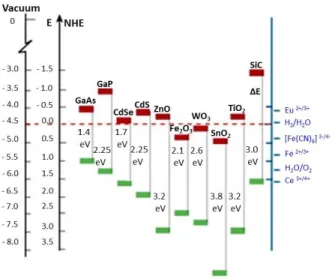
A PE is usually fabricated by depositing a thin compact layer of a wide band gap semiconducting oxide on a TCO coated glass. As shown in Figure 1-15 for applications in PV, a semiconductor should be characterized by a suitable band position for the injection of electrons from the sensitizing dye. Indeed, owning a wide band gap (Eg > 3 eV), these semiconductors are characterized
by absorption in the UV region, which implies the necessity of using a sensitizer with high extinction coefficient in the visible range.
Figure 1-15 Comparison of the lower edge of the CB (in red), upper edge of the VB (in green) and band gap energy (in eV) for various semiconductors in contact with an aqueous electrolyte at pH 1. The standard redox potentials for some redox couples are shown, as well as the standard hydrogen potential. The energy scale is indicated in eV using both the vacuum and the normal hydrogen electrode (NHE) level as a reference. Adapted from Reference 50.
For sufficient dye loading, a nanoporous film of semiconductor should be used, in order to ensure a high surface area.51 The most widely used
22 can be found in literature. ZnO, owing a similar Eg, is considered the most
promising alternative to TiO2: it is characterized by low cost, high stability
against photocorrosion and it has a high µe (115–155 cm2 V−1 s−1), which
ensures efficient electron transport in the semiconducting thin film and slow recombination rate.52 However, ZnO based DSSCs are characterized by
lower PCE compared to the TiO2 based counterparts: Memarian et al.
reported a PCE of 7.5% using ZnO polydispersed aggregates obtained by spray pyrolysis.53 The formation of insulating agglomerates of Zn2+/dye
complexes, causing the dissolution of ZnO, limits the electron injection, when acidic dyes carrying carboxylic groups are used.54 On the other hand, SnO
2
is characterized by higher Eg (3.8 eV) and µe (250 cm2 V−1 s−1 and 125cm2
V−1 s−1 for single crystal and nanostructured SnO2) compared to TiO2 (Eg 3.2
eV and µe 1 cm2 V−1 s−1),55 but the low conduction band edge energy is the
reason for the poor PV performance (PCE ~1.70%), which can be endorsed to low Voc values (~0.4 V for iodide based electrolytes).56 An alternative
strategy to boost the PV performance, while taking advantage of the reported SnO2 high µe value, is the fabrication of hybrid structures of SnO2 and TiO2:
Gu et al. reported a PCE of 7.87% when using as PE material SnO2@TiO2
core@shell nanoparticles prepared by flame spray pryrolysis.57
Thus, an ideal photoanode should have the following characteristics: • high surface area to ensure high dye loading;
• high electron mobility for a fast electron injection from the dye excited state and fast electron transfer from the dye to the external circuit;
• porous structure to facilitate the diffusion of the electrolyte; • high resistance to photocorrosion;
• high scattering of the sun light to favour the absorption from the dye of the diffused light.58
A common methodology used to match these requirements envisages four layers of anatase TiO2 with different particles sizes. A blocking underlayer
23 (thickness ~50 nm), whose role is to enhance the adhesion on TCO glass substrate and to help reducing the dark current generated by the charge recombination between the electrons in the TCO glass and the holes of the oxidized electrolyte. This is possible thanks to the reduction of the number of pores, which allow the infiltration of the electrolyte into the TiO2/TCO
interface and the formation of a compact thin layer.59, 60(Figure 1-16)
Figure 1-16 Schematic representation of A) the recombination of electrons in the FTO back contact with the oxidized form of the electrolyte and B) its suppression in the presence of the blocking underlayer.
The active layer is usually a transparent layer of mesoporous anatase TiO2
nanoparticles with a diameter of ~20 nm. The thickness of the layer varies in the range ~5-12 µm, according to the extinction coefficient of the sensitizing dye. The large surface area of the NPs ensures the adhesion of a large number of dye molecules. Among the various techniques available, screen printing is the most efficient and reproducible one, allowing the deposition of ordered multilayers with the desired thickness.
A non-transparent scattering layer can be deposited on top of the active layer, acting as a photon trapping system: the presence of larger TiO2
![Figure 1-22. Molecular structures of A) D35 (E)-3-(5-(4-(bis(2',4'-dibutoxy-[1,1'-biphenyl]-4- (E)-3-(5-(4-(bis(2',4'-dibutoxy-[1,1'-biphenyl]-4-yl)amino)phenyl)thiophen-2-yl)-2-cyanoacrylic acid), B) Y123 (3-{6-{4-[bis(2',4'- dihexyloxybiphenyl-4-yl)](https://thumb-eu.123doks.com/thumbv2/123dokorg/4589100.39074/51.774.88.692.119.681/molecular-structures-dibutoxy-biphenyl-dibutoxy-thiophen-cyanoacrylic-dihexyloxybiphenyl.webp)